
2002-2014 Microchip Technology Inc.
DS20001752C-page 1
MCP1252/3
Features:
• Inductorless, Buck/Boost, DC/DC Converter
• Low Power: 80 µA (Typical)
• High Output Voltage Accuracy:
- ±2.5% (V
OUT
Fixed)
• 120 mA Output Current
• Wide Operating Temperature Range:
- Industrial Temperature (I): -40°C to +85°C
- Extended Temperature (E): -40°C to +125°C
• Thermal Shutdown and Short-Circuit Protection
• Uses Small Ceramic Capacitors
• Switching Frequency:
- MCP1252: 650 kHz
- MCP1253: 1 MHz
• Low-Power Shutdown Mode: 0.1 µA (Typical)
• Shutdown Input Compatible with 1.8V Logic
• V
IN
Range: 2.0V to 5.5V
• Selectable Output Voltage (3.3V or 5.0V) or
Adjustable Output Voltage
• Space-Saving, 8-Lead MSOP
• Soft-Start Circuitry to Minimize In-Rush Current
• AEC-Q100 Qualified
Applications:
• White LED Backlighting
• Color Display Bias
• Local 3V-to-5V Conversions
• Flash Memory Supply Voltage
• SIM Interface Supply for GSM Phones
• Smart Card Readers
• PCMCIA Local 5V Supplies
Description:
The MCP1252/3 are inductorless, positive-regulated
charge pump DC/DC converters. The devices generate
a regulated fixed (3.3V or 5.0V) or adjustable output
voltage. They are specifically designed for applications
requiring low noise and high efficiency and are able to
deliver up to 120 mA output current. The devices allow
the input voltage to be lower or higher than the output
voltage, by automatically switching between buck/
boost operation.
The MCP1252 has a switching frequency of 650 kHz,
avoiding interference with sensitive IF bands. The
MCP1253 has a switching frequency of 1 MHz and
allows the use of smaller capacitors than the
MCP1252, thus saving board space and cost.
Both devices feature a power-good output that can be
used to detect out-of-regulation conditions. Extremely
low supply current and low external parts count (three
capacitors) make these devices ideal for small, battery-
powered applications. A shutdown mode is also pro-
vided for further power reduction. The MCP1252 and
MCP1253 feature thermal and short-circuit protection
and are offered in space-saving, 8-lead, MSOP
packages.
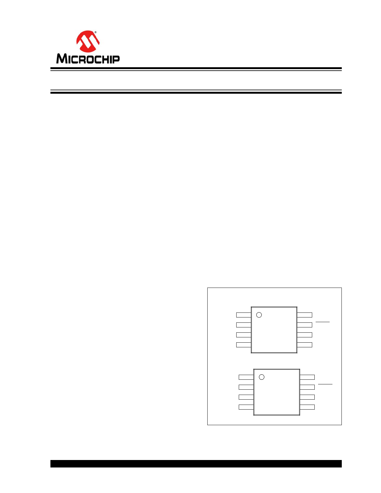
Package Types
MSOP (Fixed)
MSOP (Adjustable)
PGOOD
V
OUT
V
IN
GND
SELECT
SHDN
C+
C-
1
2
3
4
8
7
6
5
PGOOD
V
OUT
V
IN
GND
FB
SHDN
C+
C-
1
2
3
4
8
7
6
5
MCP1252
MCP1253
MCP1252
MCP1253
Low-Noise, Positive-Regulated Charge Pump
MCP1252/3
DS20001752C-page 2
2002-2014 Microchip Technology Inc.
Functional Block Diagram
PGOOD
200 mV
1.21V
84 mV
+
+
+
Switch
Control
V
OUT
V
IN
GND
C-
C+
SHDN
SELECT
MCP1252-33X50
173 k
140 k
100 k
+
-
+
-
+
-
PGOOD
200 mV
1.21V
84 mV
+
+
+
Switch
Control
V
OUT
V
IN
GND
C-
C+
SHDN
FB
MCP1252-ADJ
+
-
+
-
+
-
MCP1253-33X50
MCP1253-ADJ
2002-2014 Microchip Technology Inc.
DS20001752C-page 3
MCP1252/3
1.0
ELECTRICAL
CHARACTERISTICS
Absolute Maximum Ratings †
Power Supply Voltage, V
IN
...............................................6.0V
Voltage on Any Pin w.r.t. GND ............... -0.3V to (V
IN
+ 0.3V)
Output Short Circuit Duration ................................continuous
Storage Temperature Range .........................-65°C to +150°C
Ambient Temperature with Power Applied ....-55°C to +125°C
Junction Temperature ................................................. +150°C
ESD Ratings:
Human Body Model (1.5 k
in Series with 100 pF)4 kV
Machine Body Model (200 pF, No Series Resistance)
400V
†Notice: Stresses above those listed under “Maximum
Ratings” may cause permanent damage to the device. This is
a stress rating only and functional operation of the device at
those or any other conditions above those indicated in the
operational listings of this specification is not implied.
Exposure to maximum rating conditions for extended periods
may affect device reliability.
ELECTRICAL CHARACTERISTICS
Electrical Specifications: Unless otherwise specified, all limits are specified for T
A
= -40°C to +85°C ("I" Temperature), T
A
= -40°C
to +125°C ("E" Temperature), SHDN = V
IN
, C
IN
= C
OUT
= 10 µF, C
FLY
= 1 µF, I
OUT
= 10 mA. Typical values are for T
A
= +25°C.
Parameters
Sym.
Min.
Typ.
Max.
Units
Conditions
Selectable Output - MCP1252-33X50, MCP1253-33X50: SELECT = V
IN
, V
OUT
= 3.3V
Supply Voltage
V
IN
2.1
—
5.5
V
Output Voltage Accuracy
V
OUT
-2.5
±0.5
+2.5
%
2.3V
V
IN
< 2.5V, I
OUT
80 mA
2.5V
V
IN
5.5V, I
OUT
120 mA
Output Current
I
OUT
80
100
—
mA
2.3V
V
IN
< 2.5V
120
150
—
mA
2.5V
V
IN
5.5V
SELECT Logic Input Voltage High
V
IH
1.4
—
—
V
MCP1252-33X50, MCP1253-33X50
Selectable Output - MCP1252-33X50, MCP1253-33X50: SELECT = GND, V
OUT
= 5.0V
Supply Voltage
V
IN
2.7
—
5.5
V
Output Voltage Accuracy
V
OUT
-2.5
±0.5
+2.5
%
2.7V
V
IN
< 3.0V, I
OUT
40 mA
3.0V
V
IN
5.5V, I
OUT
120 mA
Output Current
I
OUT
40
80
—
mA
2.7V
V
IN
< 3.0V
120
150
—
3.0V
V
IN
5.5V
SELECT Logic Input Voltage Low
V
IL
—
—
0.4
V
MCP1252-33X50, MCP1253-33X50
Adjustable Output - MCP1252-ADJ, MCP1253-ADJ
Supply Voltage
V
IN
2.0
—
5.5
V
Output Voltage Adjustment Range
V
OUT
1.5
—
5.5
V
V
OUT(MAX)
< 2 x V
IN
FB Regulation Voltage
V
FB
1.18
1.21
1.24
V
MCP1252-ADJ, MCP1253-ADJ
ALL DEVICES
Supply Current
I
DD
—
60
120
µA
No load
Output Short-Circuit Current
I
SC
—
200
—
mA
V
OUT
= GND, foldback current
Shutdown Current
I
SHDN
—
0.1
2.0
µA
SHDN = 0V
Power Efficiency
—
81
—
%
V
IN
= 3.0V, V
OUT
= 5V
I
OUT
=120 mA
—
68
—
V
IN
= 3.6V, V
OUT
= 5V
I
OUT
=120 mA
SHDN Logic Input Voltage Low
V
IL
—
—
0.4
V
SHDN Logic Input Voltage High
V
IH
1.4
—
—
V
PGOOD Output Voltage
P
GOOD_VOL
—
0.01
—
V
I
PGOOD
= 0.5 mA
PGOOD Threshold Voltage
V
TH
—
0.93V
OUT
—
V
PGOOD Hysteresis
V
HYS
—
0.04V
OUT
—
V
MCP1252/3
DS20001752C-page 4
2002-2014 Microchip Technology Inc.
AC CHARACTERISTICS
TEMPERATURE SPECIFICATIONS
Electrical Specifications: Unless otherwise specified, all limits are specified for T
A
= -40°C to +85°C ("I" Temperature), T
A
= -40°C
to +125°C ("E" Temperature), SHDN = V
IN
, C
IN
= C
OUT
= 10 µF, C
FLY
= 1 µF, I
OUT
= 10 mA. Typical values are for T
A
= +25°C.
Parameters
Sym.
Min.
Typ.
Max.
Units
Conditions
Internal Oscillator Frequency
F
OSC
520
650
780
kHz
MCP1252
800
1000
1200
MCP1253
Ripple Voltage
V
RIP
—
50
—
mV
p-p
MCP1252
—
45
—
mV
p-p
MCP1253
V
OUT
Wake-Up Time From Shutdown T
WKUP
µsec
V
IN
= 3.6V, I
OUT
= 10 mA,
SHDN = V
IH(MIN)
,
V
OUT
from 0 to 90% Nominal
Regulated Output Voltage
—
200
—
SELECT = V
IN
—
300
—
SELECT = GND
Parameters
Symbol
Min.
Typ.
Max.
Units
Conditions
Temperature Ranges:
Specified Temperature Range
T
A
-40
—
+85
°C
"I" Temperature range
-40
—
+125
"E" Temperature range
Maximum Operating Junction
Temperature
T
J
—
—
+125
°C
Storage Temperature Range
T
A
-65
—
+150
°C
Thermal Package Resistances:
Thermal Resistance, 8 Pin MSOP
JA
—
206
—
°C/W
Single-Layer SEMI G42-88
board, Natural Convection
2002-2014 Microchip Technology Inc.
DS20001752C-page 5
MCP1252/3
2.0
TYPICAL PERFORMANCE CURVES
Note: Unless otherwise indicated, V
IN
= 3.6V, T
A
= 25°C, C
IN
= C
OUT
= 10
µ
F, C
FLY
= 1
µ
F, all capacitors X7R ceramic.
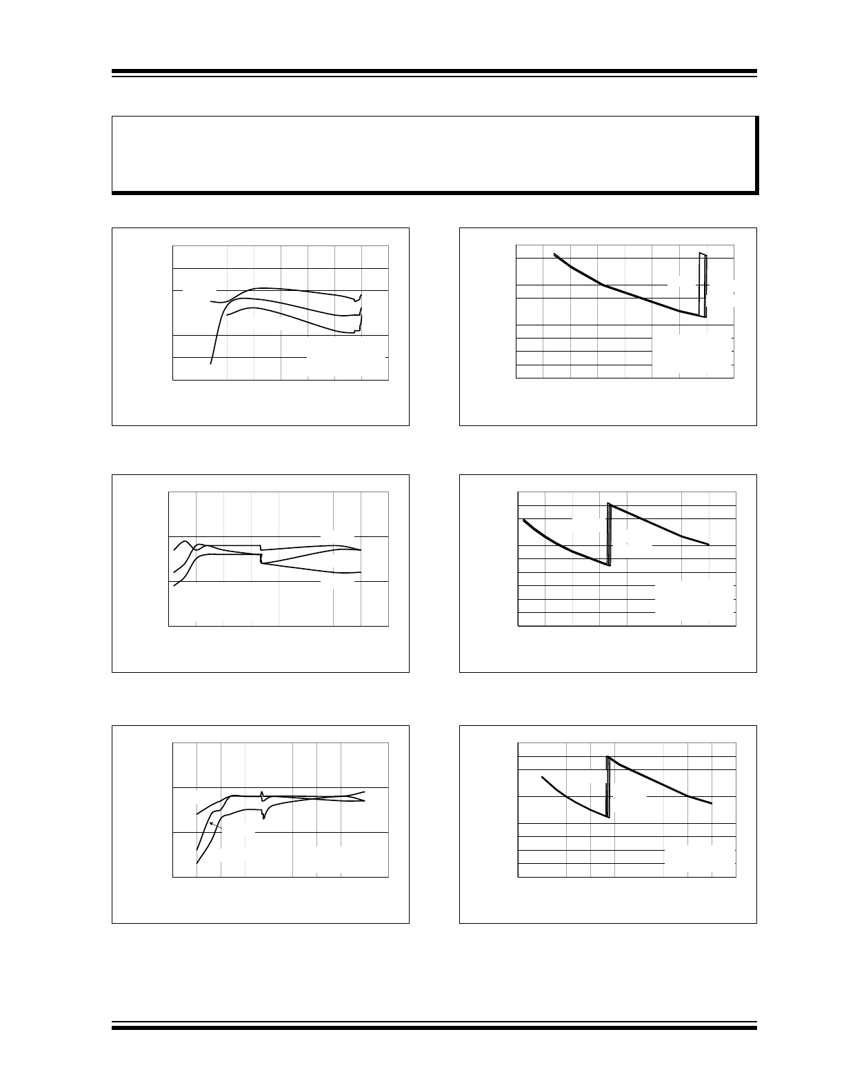
FIGURE 2-1:
Output Voltage vs. Supply
Voltage (MCP1252-33X50).
.
FIGURE 2-2:
Output Voltage vs. Supply
Voltage (MCP1252-33X50).
FIGURE 2-3:
Output Voltage vs. Supply
Voltage (MCP1252-ADJ).
FIGURE 2-4:
Percent Efficiency vs.
Supply Voltage (MCP1252-33X50).
FIGURE 2-5:
Power Efficiency vs. Supply
Voltage (MCP1252-33X50).
FIGURE 2-6:
Power Efficiency vs. Supply
Voltage
(MCP1252-ADJ).
Note:
The graphs and tables provided following this note are a statistical summary based on a limited number of
samples and are provided for informational purposes only. The performance characteristics listed herein
are not tested or guaranteed. In some graphs or tables, the data presented may be outside the specified
operating range (e.g., outside specified power supply range) and therefore outside the warranted range.
4.99
5.00
5.01
5.02
5.03
5.04
5.05
2.0
2.5
3.0
3.5
4.0
4.5
5.0
5.5
6.0
Supply Voltage (V)
Output V
o
lt
age (V
)
10 mA
80 mA
120 mA
MCP1252-33X50
SELECT = GND
V
OUT
= 5.0V
3.31
3.32
3.33
3.34
2.0
2.5
3.0
3.5
4.0
4.5
5.0
5.5
6.0
Supply Voltage (V)
Output V
o
lt
age (V
)
10 mA
80 mA
120 mA
MCP1252-33X50
SELECT = V
IN
V
OUT
= 3.3V
2.99
3.00
3.01
3.02
1.5
2.0
2.5
3.0
3.5
4.0
4.5
5.0
5.5
6.0
Supply Voltage (V)
Output V
o
lt
age (V
)
10 mA
80 mA
120 mA
MCP1252-ADJ
V
OUT
= 3.0V
0
10
20
30
40
50
60
70
80
90
100
2.0
2.5
3.0
3.5
4.0
4.5
5.0
5.5
6.0
Supply Voltage (V)
P
e
rcent E
ffi
ci
ency (%
)
10 mA
80 mA
120 mA
MCP1252-33X50
SELECT = GND
V
OUT
= 5.0V
0
10
20
30
40
50
60
70
80
90
100
2.0
2.5
3.0
3.5
4.0
4.5
5.0
5.5
6.0
Supply Voltage (V)
P
o
wer E
ffi
ci
ency (%
)
10 mA
80 mA
120 mA
MCP1252-33X50
SELECT = V
IN
V
OUT
= 3.3V
0
10
20
30
40
50
60
70
80
90
100
1.5
2.0
2.5
3.0
3.5
4.0
4.5
5.0
5.5
6.0
Supply Voltage (V)
P
o
wer E
ffi
ci
ency (%
)
10 mA
80 mA
120 mA
MCP1252-ADJ
V
OUT
= 3.0V
MCP1252/3
DS20001752C-page 6
2002-2014 Microchip Technology Inc.
Note: Unless otherwise indicated, V
IN
= 3.6V, T
A
= 25°C, C
IN
= C
OUT
= 10 mF, C
FLY
= 1 mF, all capacitors X7R ceramic.
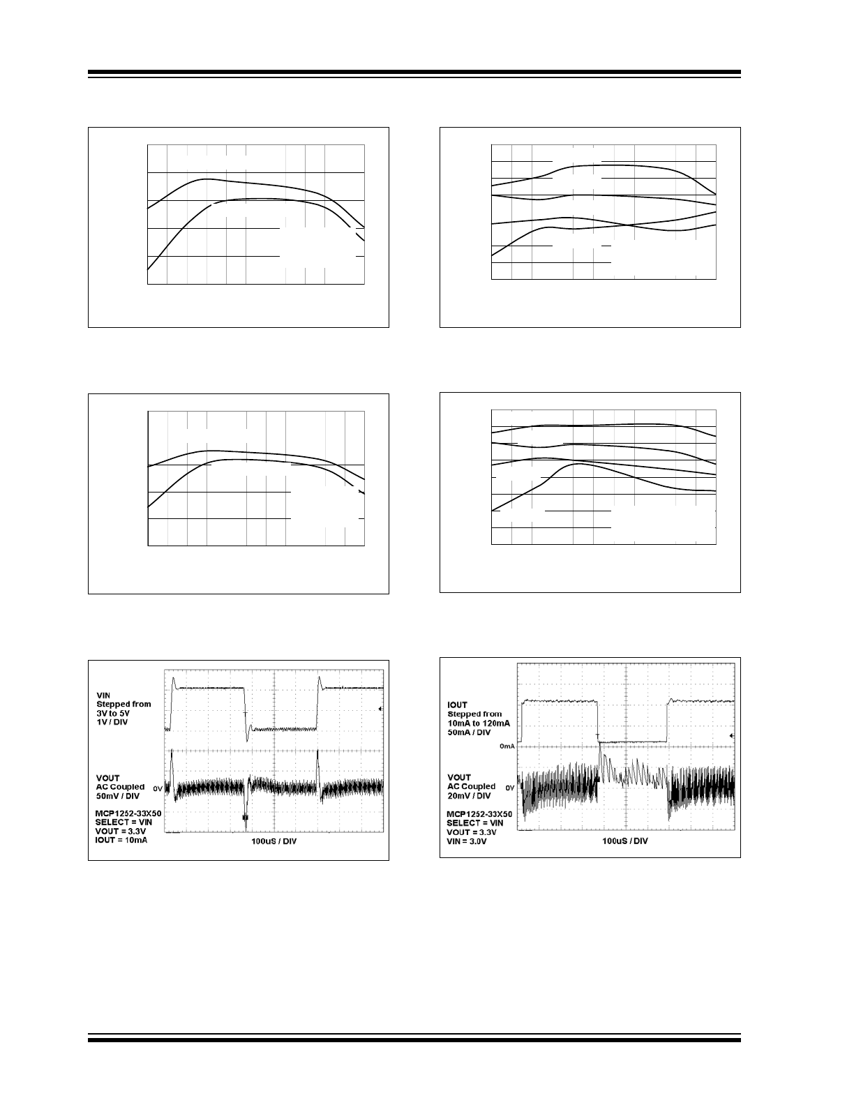
FIGURE 2-7:
Output Voltage vs.
Temperature (MCP1252-33X50,
MCP1253-33X50).
FIGURE 2-8:
Output Voltage vs.
Temperature (MCP1252-33X50,
MCP1253-33X50).
FIGURE 2-9:
Line Transient Response.
FIGURE 2-10:
Quiescent Current vs.
Temperature (MCP1253-33X50).
FIGURE 2-11:
Quiescent Current vs.
Temperature (MCP1252-33X50).
FIGURE 2-12:
Load Transient Response.
4.98
4.99
5.00
5.01
5.02
5.03
-40 -25 -10
5
20 35 50 65 80 95 110 125
Temperature (°C)
Output V
o
lt
age (V
)
MCP1252-33X50
MCP1253-33X50
SELECT = GND
V
OUT
= 5.0V
I
OUT
= 120 mA
3.28
3.29
3.30
3.31
3.32
3.33
-40 -25 -10
5
20 35 50 65 80 95 110 125
Temperature (°C)
Output V
o
lt
age (V
)
MCP1252-33X50
MCP1253-33X50
SELECT = V
IN
V
OUT
= 3.3V
I
OUT
= 120 mA
40
45
50
55
60
65
70
75
80
-40 -25 -10
5
20
35
50
65
80
95 110 125
Temperature (°C)
S
uppl
y C
u
rrent
(
u
A
)
MCP1253-33X50
SELECT = GND
V
OUT
= 5.0V, I
OUT
= 0 mA
V
IN
= 5.5V
V
IN
= 3.6V
V
IN
= 2.7V
V
IN
= 2.3V
40
45
50
55
60
65
70
75
80
-40 -25 -10
5
20
35
50
65
80
95 110 125
Temperature (°C)
S
uppl
y C
u
rrent
(
u
A
)
V
IN
= 5.5V
V
IN
= 3.6V
V
IN
= 2.7V
V
IN
= 2.3V
MCP1252-33X50
SELECT = GND
V
OUT
= 5.0V, I
OUT
= 0 mA
2002-2014 Microchip Technology Inc.
DS20001752C-page 7
MCP1252/3
Note: Unless otherwise indicated, V
IN
= 3.6V, T
A
= 25°C, C
IN
= C
OUT
= 10mF, C
FLY
= 1mF, all capacitors X7R ceramic.
FIGURE 2-13:
Output Voltage Ripple vs.
Supply Voltage (MCP1252-33X50).
FIGURE 2-14:
Output Voltage Ripple vs.
Supply Voltage (MCP1252-33X50).
FIGURE 2-15:
Start-Up (MCP1252-33X50).
FIGURE 2-16:
Output Voltage Ripple vs.
Time.
FIGURE 2-17:
Output Voltage Ripple vs.
Time.
FIGURE 2-18:
Start-Up (MCP1253-33X50).
0
10
20
30
40
50
60
70
2.0
2.5
3.0
3.5
4.0
4.5
5.0
5.5
6.0
Supply Voltage (V)
Out
put
V
o
lt
age R
ippl
e (
m
V
)
10 mA
80 mA
120 mA
MCP1252-33X50
SELECT = GND
V
OUT
= 5.0V
0
10
20
30
40
50
60
70
2.0
2.5
3.0
3.5
4.0
4.5
5.0
5.5
6.0
Supply Voltage (V)
Out
put
V
o
lt
age R
ippl
e (
m
V
)
10 mA
80 mA
120 mA
MCP1252-33X50
SELECT = V
IN
V
OUT
= 3.3V
MCP1252/3
DS20001752C-page 8
2002-2014 Microchip Technology Inc.
3.0
PIN FUNCTIONS
The descriptions of the pins are listed in
Table 3-1
.
TABLE 3-1:
PIN FUNCTION TABLE
3.1
Open-Drain Power Good Output
(PGOOD)
PGOOD is a high-impedance when the output voltage
is in regulation. A logic-low is asserted when the output
falls 7% (typical) below the nominal value. The PGOOD
output remains low until V
OUT
is within 3% (typical) of
its nominal value. On start-up, this pin indicates when
the output voltage reaches its final value. PGOOD is
high-impedance when SHDN is low.
3.2
Regulated Output Voltage (V
OUT
)
Bypass to GND with a filter capacitor.
3.3
Power Supply Input (V
IN
)
It is recommended that V
IN
be tied to a ceramic bypass
capacitor.
3.4
Ground (GND)
It is recommended that the ground pin be tied to a
ground plane for best performance.
3.5
Flying Capacitor Negative
Terminal (C-)
The charge pump capacitor (flying capacitor) is used to
transfer charge from the input supply to the regulated
output.
It is recommended that a low ESR (equivalent series
resistance) capacitor be used.
3.6
Flying Capacitor Positive Terminal
(C+)
The charge pump capacitor (flying capacitor) is used to
transfer charge from the input supply to the regulated
output.
Proper orientation is imperative when using a polarized
capacitor.
3.7
Shutdown Input (SHDN)
A logic-low signal applied to SHDN disables the device.
A logic-high signal applied to this pin allows normal
operation.
3.8
Select (SELECT) Input or
Feedback (FB) Input
MCP1252-33X50, MCP1253-33X50:
SELECT: Select Input Pin.
Connect SELECT to V
IN
for 3.3V fixed output. Connect
SELECT to GND for a 5.0V fixed output.
MCP1252-ADJ, MCP1253-ADJ:
FB: Feedback Pin.
A resistor divider connected to this pin determines the
adjustable V
OUT
value (1.5V to 5.5V).
Pin No.
Name
Function
1
PGOOD
Open-Drain Power GOOD Output
2
V
OUT
Regulated Output Voltage
3
V
IN
Power Supply Input
4
GND
Ground Terminal
5
C-
Flying Capacitor Negative Terminal
6
C+
Flying Capacitor Positive Terminal
7
SHDN
Shutdown Mode, Active-Low Input
8
SELECT
Output Voltage Select Pin (MCP1252-33X50, MCP1253-33X50)
FB
Feedback Input Pin for Adjustable Output (MCP1252-ADJ, MCP1253-ADJ)
2002-2014 Microchip Technology Inc.
DS20001752C-page 9
MCP1252/3
4.0
DEVICE OVERVIEW
4.1
Theory of Operation
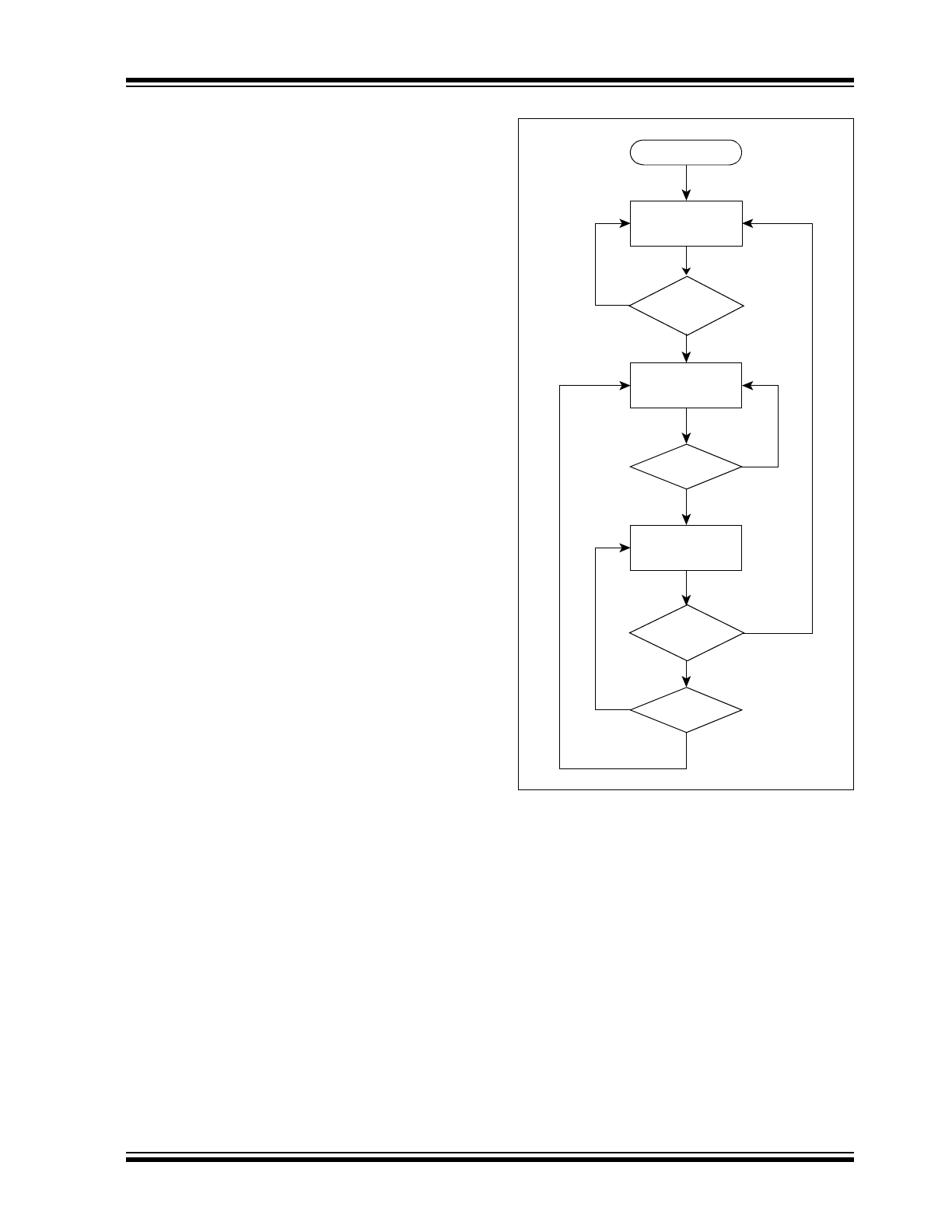
The MCP1252 and MCP1253 family of devices employ
a switched capacitor charge pump to buck or boost an
input supply voltage (V
IN
) to a regulated output voltage.
Referring to the Functional Block Diagram and
Figure 4-1
, the devices perform conversion and
regulation in three phases. When the devices are not in
shutdown mode and a steady-state condition has been
reached, the three phases are continuously cycled
through. The first phase transfers charge from the input
to the flying capacitor (C
FLY
) connected to pins C+ and
C-. This phase always occurs for half of the internal
oscillator period. During this phase, switches S
1
and S
2
are closed.
Once the first phase is complete, all switches are
opened and the second phase (idle phase) is entered.
The device compares the internal or external feedback
voltage with an internal reference. If the feedback volt-
age is below the regulation point, the device transitions
to the third phase.
The third phase transfers energy from the flying capac-
itor to the output capacitor connected to V
OUT
and the
load. If regulation is maintained, the device returns to
the idle phase. If the charge transfer occurs for half the
internal oscillator period, more charge is needed in the
flying capacitor and the device transitions back to the
first phase.
The regulation control is hysteretic, otherwise referred
to as a bang-bang control. The output is regulated
around a fixed reference with some hysteresis. As a
result, typically 50 mV of peak-to-peak ripple will be
observed at the output independent of load current.
The frequency of the output ripple, however, will be
influenced heavily by the load current and output
capacitance. The maximum frequency that will be
observed is equal to the internal oscillator frequency.
The devices automatically transition between buck or
boost operation. This provides a low-cost, compact and
simple solution for step-down/step-up DC/DC
conversion. This is especially true for battery-operated
applications that require a fixed output above or below
the input.
FIGURE 4-1:
Flow Algorithm.
START
PHASE 1:
Charge Transfer
From V
IN
to C
FLY
PHASE 2:
Idle State
V
FB
> V
REF
PHASE 3:
Charge Transfer
From C
FLY
to C
OUT
No
Yes
No
Yes
Yes
No
No
Yes
V
FB
> V
REF
t
1
1
2F
OSC
----------------
=
t
3
1
2F
OSC
----------------
=
MCP1252/3
DS20001752C-page 10
2002-2014 Microchip Technology Inc.
4.2
Power Efficiency
The power efficiency,
, is determined by the mode of
operation. In boost mode, the efficiency is
approximately half of a linear regulator. In buck mode,
the efficiency is approximately equal to that of a linear
regulator. The following formulas can be used to
approximate the power efficiency with any significant
amount of output current. At light loads, the quiescent
current of the device must be taken into consideration.
EQUATION 4-1:
4.3
Shutdown Mode
Driving SHDN low places the MCP1252 or MCP1253 in
a low-power shutdown mode. This disables the charge
pump switches, oscillator and control logic, reducing
the quiescent current to 0.1 µA (typical). The PGOOD
output is in a high-impedance state during shutdown.
4.4
PGOOD Output
The PGOOD output is an open-drain output that sinks
current when the regulator output voltage falls below
0.93V
OUT
(typical). The output voltage can either be
fixed when the selectable output device is chosen
(MCP1252-33X50, MCP1253-33X50) or adjustable
from an external resistive divider when the adjustable
device is chosen (MCP1252-ADJ, MCP1253-ADJ). If
the regulator output voltage falls below 0.93V
OUT
(typical) for less than 200 µsec and then recovers,
glitch-immunity circuits prevent the PGOOD signal
from transitioning low. A 10 k
to 1 M pull-up resistor
from PGOOD to V
OUT
may be used to provide a logic
output. Connect PGOOD to GND or leave unconnected
if not used.
4.5
Soft-Start and Short-Circuit
Protection
The MCP1252 and MCP1253 feature foldback short-
circuit protection. This circuitry provides an internal
soft-start function by limiting in-rush current during
startup and also limits the output current to 200 mA
(typical) if the output is shorted to GND. The internal
soft-start circuitry requires approximately 300 µsec,
typical with a 5V output, from either initial power-up or
release from shutdown for the output voltage to be in
regulation.
4.6
Thermal Shutdown
The MCP1252 and MCP1253 feature thermal
shutdown with temperature hysteresis. When the die
temperature exceeds 160°C, typically, the device shuts
down. When the die cools by 15°C, typically, the device
automatically turns back on. If high die temperature is
caused by output overload and the load is not removed,
the device will turn on and off, resulting in a pulse
output.
5.0
APPLICATIONS
The MCP1252 and MCP1253 are inductorless,
positive-regulated, charge pump DC/DC converters. A
typical circuit configuration for the fixed output version
is depicted in
Figure 5-1
. The adjustable version is
depicted in
Figure 5-2
.
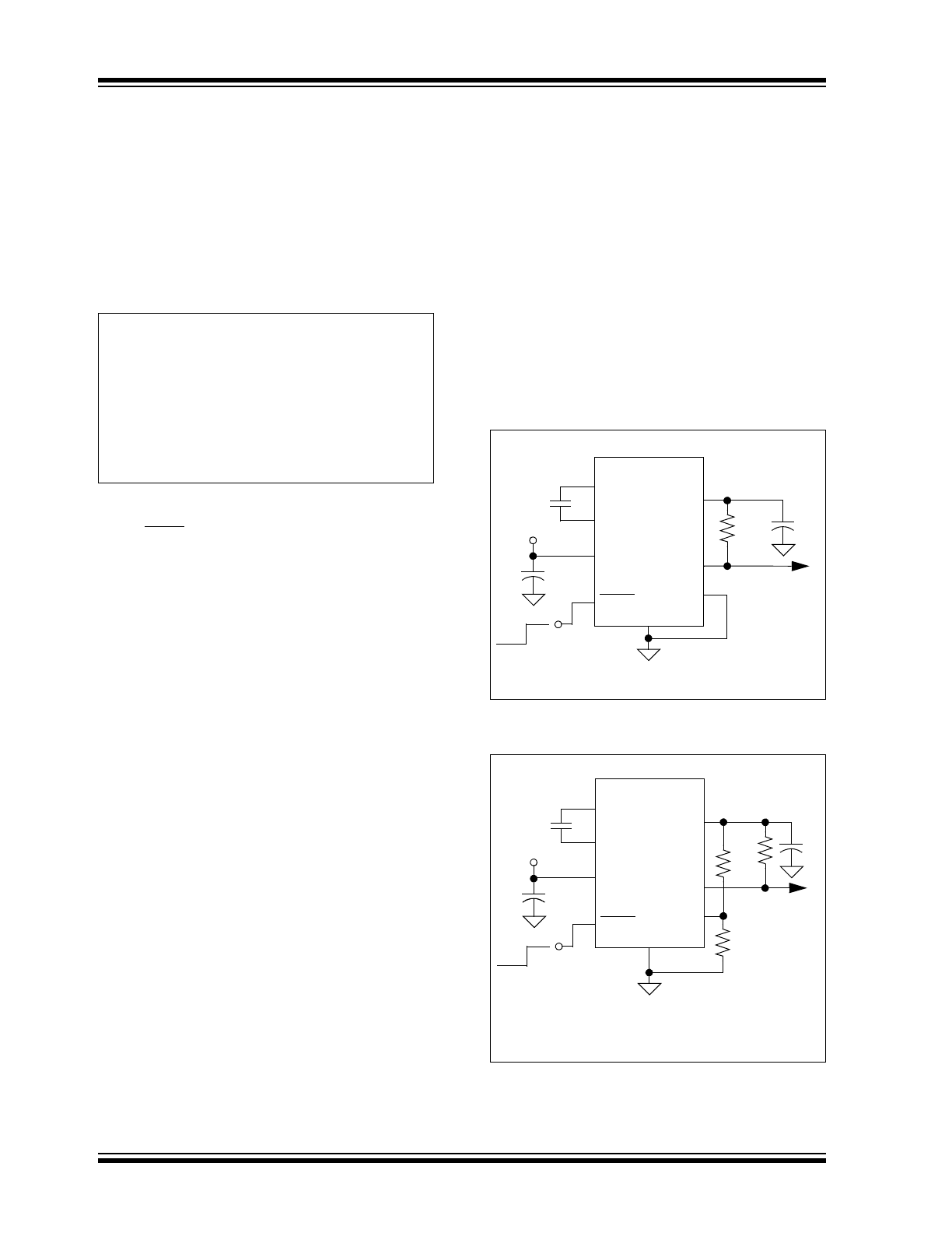
FIGURE 5-1:
Typical Circuit Configuration
for Fixed Output Device.
FIGURE 5-2:
Typical Circuit Configuration
for Adjustable Output Device.
BOOST
P
OUT
P
IN
-------------
V
OUT
I
OUT
V
IN
2
I
OUT
------------------------------------
V
OUT
V
IN
2
------------------
=
=
=
BUC K
P
OUT
P
IN
-------------
V
OUT
I
OUT
V
IN
I
OUT
--------------------------------
V
OUT
V
IN
-------------
=
=
=
MCP1252-33X50
C+
C
FLY
6
5
C-
V
IN
SHDN
3
7
OFF
ON
Shutdown
Control
+
2.7V to 5.5V
C
IN
GND
SELECT
PGOOD
V
OUT
8
1
2
+
C
OUT
R
PU
PGOOD Flag
To PIC
®
+5.0V ±2.5%
SELECTABLE OUTPUT VOLTAGE
4
C
FLY
=
1 µF
C
IN
=
10 µF
C
OUT
=
10 µF
Microcontroller
R
PU
=
100 k
MCP1252-ADJ
C+
C
FLY
6
5
C-
V
IN
SHDN
3
7
OFF
ON
Shutdown
Control
+
2.7V to 5.5V
C
IN
GND
FB
PGOOD
V
OUT
8
1
2
+
C
OUT
R
PU
PGOOD Flag
To PIC
®
+4.0V
ADJUSTABLE OUTPUT VOLTAGE
R
2
R
1
4
V
OUT
= 1.21V (1 + R
1
/R
2
)
Microcontroller
C
FLY
=
1 µF
C
IN
=
10 µF
C
OUT
=
10 µF
R
PU
=
100 k
R
1
=
23.2 k
R
2
=
10 k
+