2004-2014 Microchip Technology Inc.
DS20001906D-page 1
MCP102/103/121/131
Features:
• Ultra-Low Supply Current: 1.75 µA
(steady-state maximum)
• Precision Monitoring Options of:
- 1.90V, 2.32V, 2.63V, 2.93V, 3.08V, 4.38V and
4.63V
• Resets Microcontroller in a Power-Loss Event
• RST Pin (active-low):
- MCP121: Active-low, Open-drain
- MCP131: Active-low, Open-drain with Inter-
nal Pull-up Resistor
- MCP102 and MCP103: Active-low, Push-pull
• Reset Delay Timer (120 ms delay, typical)
• Available in SOT-23, TO-92 and SC70 Packages
• Temperature Range:
- Extended: -40°C to +125°C
(except MCP1XX-195)
- Industrial: -40°C to +85°C (MCP1XX-195 only)
• Pb-free Devices
Applications:
• Critical Microcontroller and Microprocessor
Power-monitoring Applications
• Computers
• Intelligent Instruments
• Portable Battery-powered Equipment
General Description:
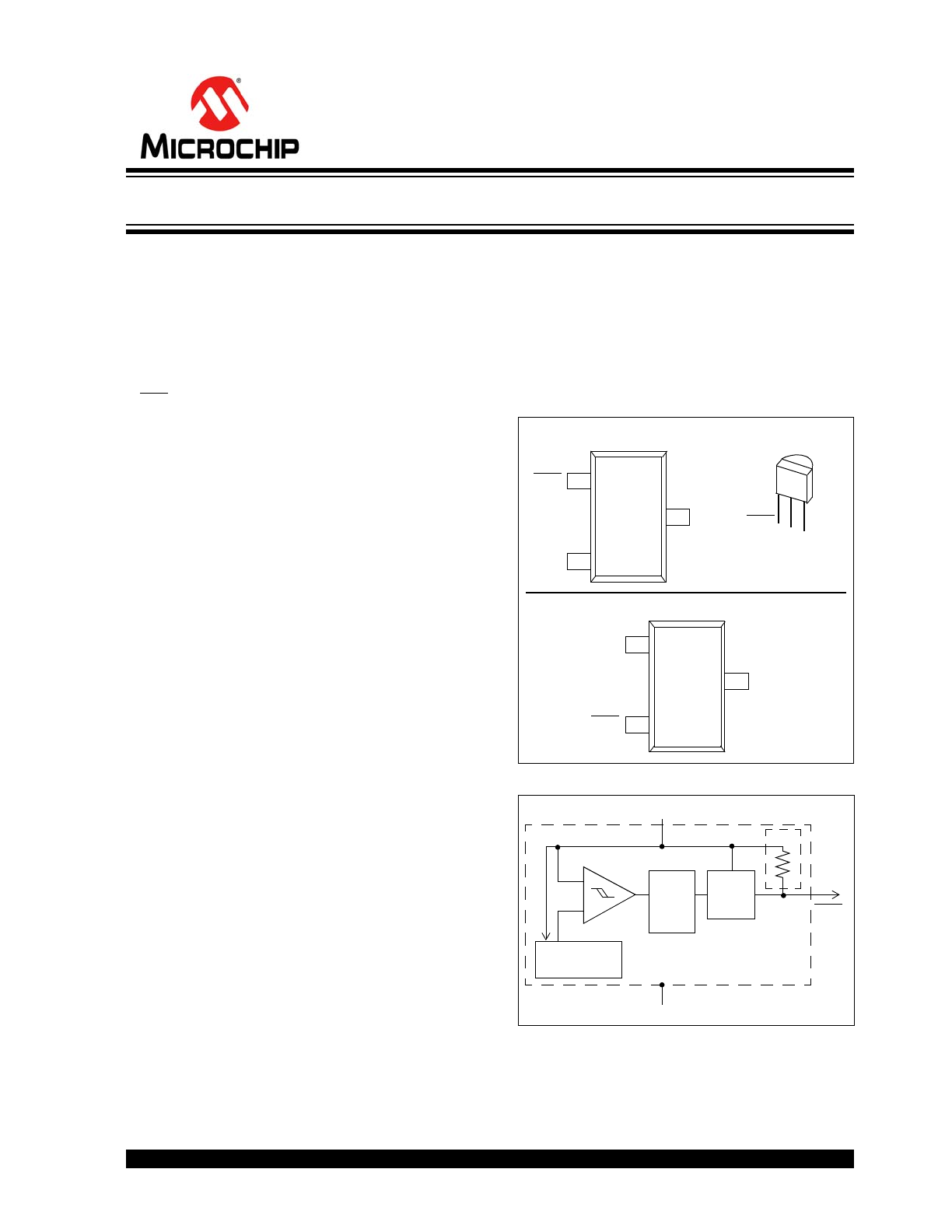
The MCP102/103/121/131 devices are voltage
supervisor devices designed to keep a microcontroller
in reset until the system voltage has reached and
stabilized at the proper level for reliable system
operation.
Table 1
shows the available features for
these devices.
Package Types
Block Diagram
SOT-23/SC70
V
SS
RST
M
C
P102
/12
1
/1
31
1
2
3
V
DD
RST
TO-92
SOT-23/SC70
V
DD
V
SS
MC
P
1
03
1
2
3
RST
V
DD
V
SS
V
DD
Comparator
+
–
Output
Driver
RST
Band Gap
Reference
V
SS
Reset
Delay
Circuit
R
(1)
Note:
MCP131 only
Micropower Voltage Supervisors

MCP102/103/121/131
DS20001906D-page 2
2004-2014 Microchip Technology Inc.
TABLE 1:
DEVICE FEATURES
Device
Output
Reset
Delay
(typ)
Package Pinout
(Pin # 1, 2, 3)
Comment
Type
Pull-up Resistor
MCP102 Push-pull
No
120 ms
RST, V
DD
, V
SS
MCP103 Push-pull
No
120 ms
V
SS
, RST, V
DD
MCP121 Open-drain External
120 ms
RST, V
DD
, V
SS
MCP131 Open-drain Internal (~95 k
) 120 ms
RST, V
DD
, V
SS
MCP111 Open-drain External
No
V
OUT
, V
SS
, V
DD
See MCP111/112 Data Sheet
(DS21889)
MCP112 Push-Pull
No
No
V
OUT
, V
SS
, V
DD
See MCP111/112 Data Sheet
(DS21889)

2004-2014 Microchip Technology Inc.
DS20001906D-page 3
MCP102/103/121/131
1.0
ELECTRICAL CHARACTERISTICS
Absolute Maximum Ratings†
V
DD
. . . . . . . . . . . . . . . . . . . . . . . . . . . . . . . . . . . . . . . . . . . . . . . . . . . . . . . . . . . . . . . . . . . . . . . . . . . . . . . . . . . . . . 7.0V
Input current (V
DD
) . . . . . . . . . . . . . . . . . . . . . . . . . . . . . . . . . . . . . . . . . . . . . . . . . . . . . . . . . . . . . . . . . . . . . . . . . 10 mA
Output current (RST) . . . . . . . . . . . . . . . . . . . . . . . . . . . . . . . . . . . . . . . . . . . . . . . . . . . . . . . . . . . . . . . . . . . . . . . 10 mA
Rated Rise Time of V
DD
. . . . . . . . . . . . . . . . . . . . . . . . . . . . . . . . . . . . . . . . . . . . . . . . . . . . . . . . . . . . . . . . . . . 100V/µs
All inputs and outputs (except RST) w.r.t. V
SS
. . . . . . . . . . . . . . . . . . . . . . . . . . . . . . . . . . . . . . . . -0.6V to (V
DD
+ 1.0V)
RST output w.r.t. V
SS
. . . . . . . . . . . . . . . . . . . . . . . . . . . . . . . . . . . . . . . . . . . . . . . . . . . . . . . . . . . . . . . . -0.6V to 13.5V
Storage temperature . . . . . . . . . . . . . . . . . . . . . . . . . . . . . . . . . . . . . . . . . . . . . . . . . . . . . . . . . . . . . . . -65°C to + 150°C
Ambient temperature with power applied . . . . . . . . . . . . . . . . . . . . . . . . . . . . . . . . . . . . . . . . . . . . . . . -40°C to + 125°C
Maximum Junction temperature with power applied . . . . . . . . . . . . . . . . . . . . . . . . . . . . . . . . . . . . . . . . . . . . . . . . 150°C
ESD protection on all pins. . . . . . . . . . . . . . . . . . . . . . . . . . . . . . . . . . . . . . . . . . . . . . . . . . . . . . . . . . . . . . . . . . . . ³ 2 kV
† Notice: Stresses above those listed under “Maximum Ratings” may cause permanent damage to the device. This is
a stress rating only and functional operation of the device at those or any other conditions above those indicated in the
operational listings of this specification is not implied. Exposure to maximum rating conditions for extended periods may
affect device reliability.
DC CHARACTERISTICS
Electrical Specifications: Unless otherwise indicated, all limits are specified for: V
DD
= 1V to 5.5V, R
PU
= 100 k
(MCP121 only),
T
A
= -40°C to +125°C.
Parameters
Sym.
Min.
Typ.
Max.
Units
Conditions
Operating Voltage Range
V
DD
1.0
—
5.5
V
Specified V
DD
Value to RST low
V
DD
1.0
—
V
I
RST
= 10 µA, V
RST
< 0.2V
Operating Current
MCP102,
MCP103,
MCP121
I
DD
—
< 1
1.75
µA
Reset Power-up Timer (t
RPU
) Inactive
—
—
20.0
µA
Reset Power-up Timer (t
RPU
) Active
MCP131
I
DD
—
< 1
1.75
µA
V
DD
> V
TRIP
and Reset Power-up
Timer (t
RPU
) Inactive
—
—
75
µA
V
DD
< V
TRIP
and Reset Power-up
Timer (t
RPU
) Inactive (
Note 3
)
—
—
90
µA
Reset Power-up Timer (t
RPU
) Active
(
Note 4
)
Note
1:
Trip point is ±1.5% from typical value.
2:
Trip point is ±2.5% from typical value.
3:
RST output is forced low. There is a current through the internal pull-up resistor.
4:
This includes the current through the internal pull-up resistor and the reset power-up timer.
5:
This specification allows this device to be used in PIC
®
microcontroller applications that require In-Circuit Serial
Programming™ (ICSP™) (see device-specific programming specifications for voltage requirements). This specification
DOES NOT allow a continuous high voltage to be present on the open-drain output pin (V
OUT
). The total time that the
V
OUT
pin can be above the maximum device operational voltage (5.5V) is 100s. Current into the V
OUT
pin should be
limited to 2 mA and it is recommended that the device operational temperature be maintained between 0°C to 70°C
(+25°C preferred). For additional information, please refer to
Figure 2-33
.
6:
This parameter is established by characterization and not 100% tested.

MCP102/103/121/131
DS20001906D-page 4
2004-2014 Microchip Technology Inc.
V
DD
Trip Point
MCP1XX-195
V
TRIP
1.872
1.900
1.929
V
T
A
= +25°C (
Note 1
)
1.853
1.900
1.948
V
T
A
= -40°C to +85°C (
Note 2
)
MCP1XX-240
2.285
2.320
2.355
V
T
A
= +25°C (
Note 1
)
2.262
2.320
2.378
V
Note 2
MCP1XX-270
2.591
2.630
2.670
V
T
A
= +25°C (
Note 1
)
2.564
2.630
2.696
V
Note 2
MCP1XX-300
2.886
2.930
2.974
V
T
A
= +25°C (
Note 1
)
2.857
2.930
3.003
V
Note 2
MCP1XX-315
3.034
3.080
3.126
V
T
A
= +25°C (
Note 1
)
3.003
3.080
3.157
V
Note 2
MCP1XX-450
4.314
4.380
4.446
V
T
A
= +25°C (
Note 1
)
4.271
4.380
4.490
V
Note 2
MCP1XX-475
4.561
4.630
4.700
V
T
A
= +25°C (
Note 1
)
4.514
4.630
4.746
V
Note 2
V
DD
Trip Point Tempco
T
TPCO
—
±100
—
ppm/°C
Threshold
Hysteresis
min. = 1%,
max = 6%)
MCP1XX-195
V
HYS
0.019
—
0.114
V
T
A
= +25°C
MCP1XX-240
0.023
—
0.139
V
MCP1XX-270
0.026
—
0.158
V
MCP1XX-300
0.029
—
0.176
V
MCP1XX-315
0.031
—
0.185
V
MCP1XX-450
0.044
—
0.263
V
MCP1XX-475
0.046
—
0.278
V
RST Low-level Output Voltage
V
OL
—
—
0.4
V
I
OL
= 500 µA, V
DD
= V
TRIP(MIN)
RST High-level Output Voltage
(MCP102 and MCP103 only)
V
OH
V
DD
– 0.6
—
—
V
I
OH
= 1 mA; for MCP102/MCP103 only
(push-pull output)
Internal Pull-up Resistor
(MCP131 only)
R
PU
—
95
—
k
V
DD
= 5.5V
Open-drain High Voltage on Output
(MCP121 only)
V
ODH
—
—
13.5
(5)
V
V
DD
= 3.0V, Time voltage > 5.5V
applied
100s,
current into pin limited to 2 mA, 25°C
operation recommended
(
Note 5
,
Note 6
)
Open-drain Output Leakage Current
(MCP121 only)
I
OD
—
0.1
—
µA
DC CHARACTERISTICS (CONTINUED)
Electrical Specifications: Unless otherwise indicated, all limits are specified for: V
DD
= 1V to 5.5V, R
PU
= 100 k
(MCP121 only),
T
A
= -40°C to +125°C.
Parameters
Sym.
Min.
Typ.
Max.
Units
Conditions
Note
1:
Trip point is ±1.5% from typical value.
2:
Trip point is ±2.5% from typical value.
3:
RST output is forced low. There is a current through the internal pull-up resistor.
4:
This includes the current through the internal pull-up resistor and the reset power-up timer.
5:
This specification allows this device to be used in PIC
®
microcontroller applications that require In-Circuit Serial
Programming™ (ICSP™) (see device-specific programming specifications for voltage requirements). This specification
DOES NOT allow a continuous high voltage to be present on the open-drain output pin (V
OUT
). The total time that the
V
OUT
pin can be above the maximum device operational voltage (5.5V) is 100s. Current into the V
OUT
pin should be
limited to 2 mA and it is recommended that the device operational temperature be maintained between 0°C to 70°C
(+25°C preferred). For additional information, please refer to
Figure 2-33
.
6:
This parameter is established by characterization and not 100% tested.
2004-2014 Microchip Technology Inc.
DS20001906D-page 5
MCP102/103/121/131
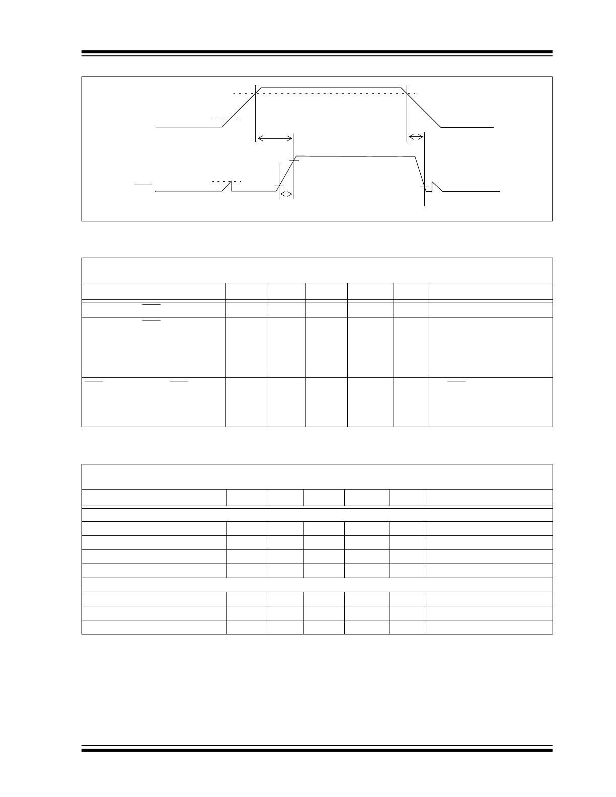
FIGURE 1-1:
Timing Diagram.
AC CHARACTERISTICS
Electrical Specifications: Unless otherwise indicated, all limits are specified for: V
DD
= 1V to 5.5V, R
PU
= 100 k
(MCP121 only), T
A
= -40°C to +125°C.
Parameters
Sym.
Min.
Typ.
Max.
Units
Conditions
V
DD
Detect to RST Inactive
t
RPU
80
120
180
ms
Figure 1-1
and C
L
= 50 pF
V
DD
Detect to RST Active
t
RPD
—
130
—
µs
V
DD
ramped from
V
TRIP(MAX)
+ 250 mV down to
V
TRIP(MIN)
– 250 mV, per
Figure 1-1
,
C
L
= 50 pF (
Note 1
)
RST Rise Time After RST Active
(MCP102 and MCP103 only)
t
RT
—
5
—
µs
For RST 10% to 90% of final
value per
Figure 1-1
,
C
L
= 50 pF
(
Note 1
)
Note 1:
These parameters are for design guidance only and are not 100% tested.
TEMPERATURE CHARACTERISTICS
Electrical Specifications: Unless otherwise noted, all limits are specified for: V
DD
= 1V to 5.5V, R
PU
= 100 k
(MCP121 only), T
A
= -40°C to +125°C.
Parameters
Sym.
Min.
Typ.
Max.
Units
Conditions
Temperature Ranges
Specified Temperature Range
T
A
-40
—
+85
ºC
MCP1XX-195
Specified Temperature Range
T
A
-40
—
+125
ºC
Except MCP1XX-195
Maximum Junction Temperature
T
J
—
—
+150
ºC
Storage Temperature Range
T
A
-65
—
+150
ºC
Package Thermal Resistances
Thermal Resistance, 3L-SOT-23
JA
—
308
—
ºC/W
Thermal Resistance, 3L-SC70
JA
—
335
—
ºC/W
Thermal Resistance, 3L-TO-92
JA
—
146
—
ºC/W
1V
1V
V
TRIP
V
DD
RST
t
RPU
V
OH
t
RT
t
RPD
V
OL
MCP102/103/121/131
DS20001906D-page 6
2004-2014 Microchip Technology Inc.
2.0
TYPICAL PERFORMANCE CURVES
Note: Unless otherwise indicated, all limits are specified for: V
DD
= 1V to 5.5V, R
PU
= 100 k
(MCP121 only;
see
Figure 4-1
), T
A
= -40°C to +125°C.
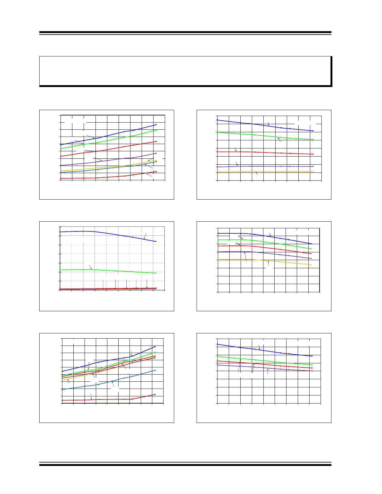
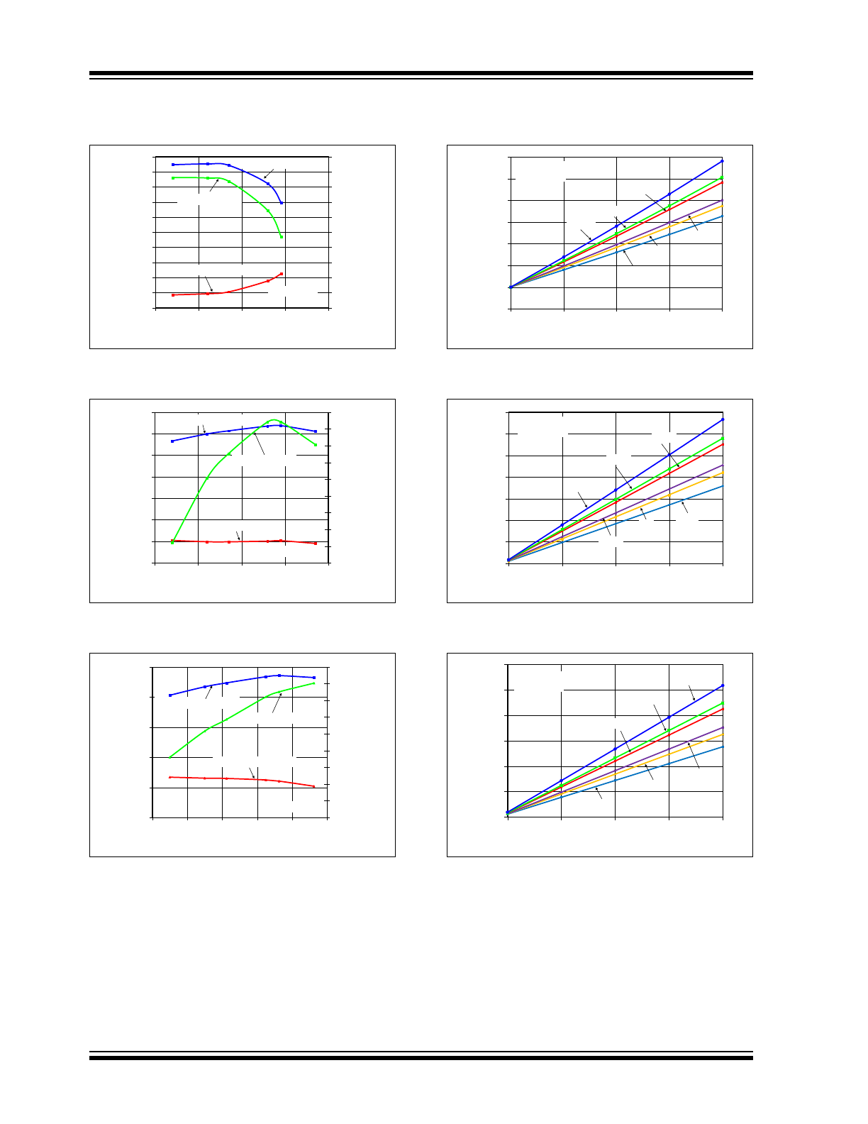
FIGURE 2-1:
I
DD
vs. Temperature
(Reset Power-up Timer Inactive) (MCP102-195).
FIGURE 2-2:
I
DD
vs. Temperature
(Reset Power-up Timer Inactive) (MCP131-315).
FIGURE 2-3:
I
DD
vs. Temperature
(Reset Power-up Timer Inactive) (MCP121-450).
FIGURE 2-4:
I
DD
vs. Temperature
(Reset Power-up Timer Active) (MCP102-195).
FIGURE 2-5:
I
DD
vs. Temperature
(Reset Power-up Timer Active) (MCP131-315).
FIGURE 2-6:
I
DD
vs. Temperature
(Reset Power-up Timer Active) (MCP121-450).
Note:
The graphs and tables provided following this note are a statistical summary based on a limited number of
samples and are provided for informational purposes only. The performance characteristics listed herein
are not tested or guaranteed. In some graphs or tables, the data presented may be outside the specified
operating range (e.g., outside specified power supply range) and therefore outside the warranted range.
0
0.2
0.4
0.6
0.8
1
1.2
1.4
1.6
1.8
-40
-20
0
20
40
60
80
100
120
140
I
DD
(µA)
Temperature (°C)
1.7V
1.0V
2.1V
2.8V
4.0V
5.0V
5.5V
MCP102-195
0
5
10
15
20
25
30
35
-40
-20
0
20
40
60
80
100
120
140
I
DD
(µA)
Temperature (°C)
1.0V
2.9V
MCP131-315
3.3V
5.5V
5.0V
4.0V
4.5V
0
0.1
0.2
0.3
0.4
0.5
0.6
0.7
0.8
0.9
-40
-20
0
20
40
60
80
100
120
140
I
DD
(µA)
Temperature (°C)
3.0V
1.0V
4.6V
4.1V
5.0V
5.5V
MCP121-450
4.8V
0
2
4
6
8
10
12
14
16
-40
-20
0
20
40
60
80
100
120
140
I
DD
(µA)
Temperature (°C)
2.1V
2.8V
4.0V
5.0V
5.5V
MCP102-195
0
10
20
30
40
50
60
70
80
-40
-20
0
20
40
60
80
100
120
140
I
DD
(µA)
Temperature (°C)
3.3V
4.0V
4.5V
5.0V
MCP131-315
5.5V
0
2
4
6
8
10
12
14
16
-40
-20
0
20
40
60
80
100
120
140
I
DD
(µA)
Temperature (°C)
4.6V
5.0V
5.5V
MCP121-450
4.8V
2004-2014 Microchip Technology Inc.
DS20001906D-page 7
MCP102/103/121/131
Note: Unless otherwise indicated, all limits are specified for: V
DD
= 1V to 5.5V, R
PU
= 100 k
(MCP121 only;
see
Figure 4-1
), T
A
= -40°C to +125°C.
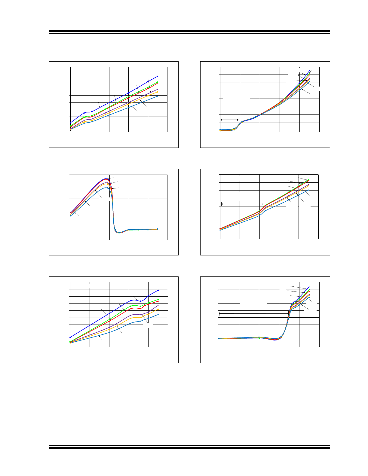
FIGURE 2-7:
I
DD
vs. V
DD
(Reset Power-up Timer Inactive) (MCP102-195).
FIGURE 2-8:
I
DD
vs. V
DD
(Reset Power-up Timer Inactive) (MCP131-315).
FIGURE 2-9:
I
DD
vs. V
DD
(Reset Power-up Timer Inactive) (MCP121-450).
FIGURE 2-10:
I
DD
vs.V
DD
(Reset Power-up Timer Active) (MCP102-195).
FIGURE 2-11:
I
DD
vs.V
DD
(Reset Power-up Timer Active) (MCP131-315).
FIGURE 2-12:
I
DD
vs.V
DD
(Reset Power-up Timer Active) (MCP121-450).
0
0.2
0.4
0.6
0.8
1
1.2
1.4
1.6
1.8
1.0
2.0
3.0
4.0
5.0
6.0
I
DD
(µA)
V
DD
(V)
-40°C
+25°C
+85°C
+125°C
MCP102-195
0°C
+70°C
-5
0
5
10
15
20
25
30
35
1.0
2.0
3.0
4.0
5.0
6.0
I
DD
(µA)
V
DD
(V)
MCP131-315
-40°C
+85°C
+125°C
0°C
+70°C
+25°C
0
0.1
0.2
0.3
0.4
0.5
0.6
0.7
0.8
0.9
1.0
2.0
3.0
4.0
5.0
6.0
I
DD
(µA)
V
DD
(V)
MCP121-450
-40°C
+25°C
+85°C
+125°C
0°C
+70°C
0
2
4
6
8
10
12
14
16
1.0
2.0
3.0
4.0
5.0
6.0
I
DD
(µA)
V
DD
(V)
0°C
-40°C
MCP102-195
Device in Reset
t
RPU
inactive
+125°C
+85°C
+70°C
+25°C
0
10
20
30
40
50
60
70
80
1.0
2.0
3.0
4.0
5.0
6.0
I
DD
(µA)
V
DD
(V)
MCP131-315
-40°C
+25°C
+85°C
+125°C
+70°C
Device in Reset
t
RPU
inactive
0°C
-2
0
2
4
6
8
10
12
14
16
1.0
2.0
3.0
4.0
5.0
6.0
I
DD
(µA)
V
DD
(V)
MCP121-450
-40°C
+25°C
+85°C
+125°C
0°C
+70°C
Device in Reset
t
RPU
inactive
MCP102/103/121/131
DS20001906D-page 8
2004-2014 Microchip Technology Inc.
Note: Unless otherwise indicated, all limits are specified for: V
DD
= 1V to 5.5V, R
PU
= 100 k
(MCP121;
see
Figure 4-1
), T
A
= -40°C to +125°C.
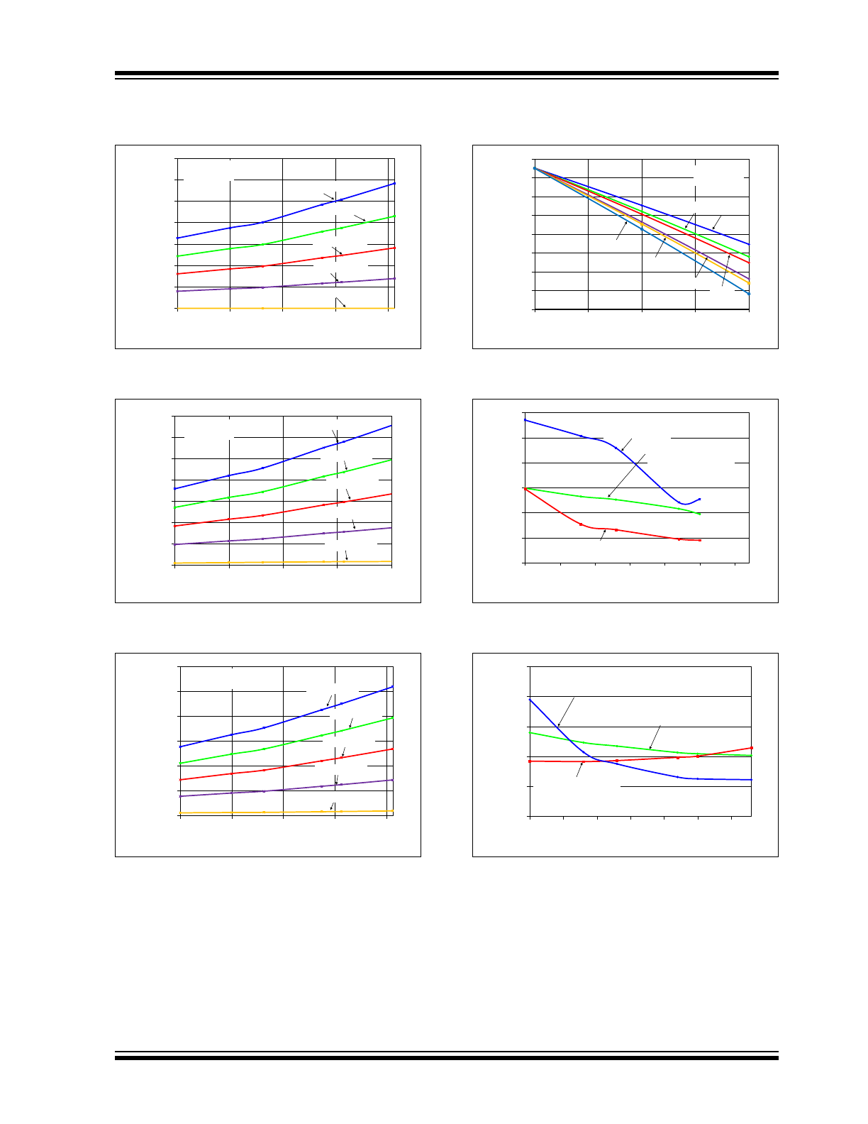
FIGURE 2-13:
V
TRIP
vs. Temperature vs.
Hysteresis (MCP102-195).
FIGURE 2-14:
V
TRIP
vs. Temperature vs.
Hysteresis (MCP131-315).
FIGURE 2-15:
V
TRIP
vs. Temperature vs.
Hysteresis (MCP121-450).
FIGURE 2-16:
V
OL
vs. I
OL
(MCP102-195 @ V
DD
= 1.7V).
FIGURE 2-17:
V
OL
vs. I
OL
(MCP131-315 @ V
DD
= 2.9V).
FIGURE 2-18:
V
OL
vs. I
OL
(MCP121-450 @ V
DD
= 4.1V).
0.000
0.005
0.010
0.015
0.020
0.025
0.030
0.035
0.040
0.045
0.050
1.895
1.900
1.905
1.910
1.915
1.920
1.925
1.930
1.935
1.940
1.945
-60
-10
40
90
140
Hy
st (V)
V
TRIP
(V)
Temperature (°C)
V
TRIP
, decreasing V
DD
V
HYS
, Hysteresis
MCP102-195
V
TRIP
, increasing V
DD
0.090
0.092
0.094
0.096
0.098
0.100
0.102
0.104
0.106
0.108
3.060
3.080
3.100
3.120
3.140
3.160
3.180
3.200
-60
-10
40
90
140
Hy
st (V)
V
TRIP
(V)
Temperature (°C)
MCP131-315
V
TRIP
, decreasing V
DD
V
TRIP
, increasing V
DD
V
HYS
, Hysteresis
0.100
0.110
0.120
0.130
0.140
0.150
0.160
0.170
0.180
0.190
4.300
4.350
4.400
4.450
4.500
4.550
-60
-20
20
60
100
140
Hy
st (V)
V
TRIP
(V)
Temperature (°C)
MCP121-450
V
TRIP
, decreasing V
DD
V
TRIP
, increasing V
DD
V
HYS
, Hysteresis
-0.020
0.000
0.020
0.040
0.060
0.080
0.100
0.120
0.00
0.25
0.50
0.75
1.00
V
OL
(V)
I
OL
(mA)
-40°C
0°C
+85°C
+125°C
MCP102-195
V
DD
= 1.7V
+70°C
+25°C
0.000
0.010
0.020
0.030
0.040
0.050
0.060
0.070
0.00
0.25
0.50
0.75
1.00
V
OL
(V)
I
OL
(mA)
MCP131-315
V
DD
= 2.9V
-40°C
+25°C
+85°C
+125°C
+70°C
0°C
0.000
0.010
0.020
0.030
0.040
0.050
0.060
0.00
0.25
0.50
0.75
1.00
V
OL
(V)
I
OL
(mA)
MCP121-450
V
DD
= 4.1V
-40°C
+25°C
+85°C
+125°C
+70°C
0°C
2004-2014 Microchip Technology Inc.
DS20001906D-page 9
MCP102/103/121/131
Note: Unless otherwise indicated, all limits are specified for: V
DD
= 1V to 5.5V, R
PU
= 100 k
(MCP121 only;
see
Figure 4-1
), T
A
= -40°C to +125°C.
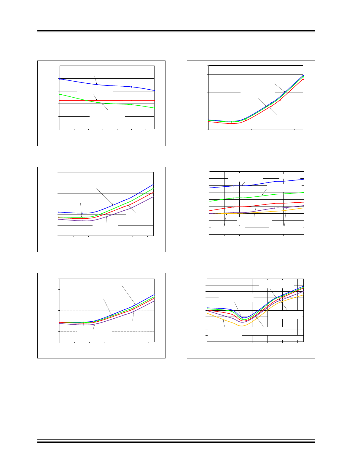
FIGURE 2-19:
V
OL
vs. Temperature
(MCP102-195 @ V
DD
= 1.7V).
FIGURE 2-20:
V
OL
vs. Temperature
(MCP131-315 @ V
DD
= 2.9V).
FIGURE 2-21:
V
OL
vs. Temperature
(MCP121-450 @ V
DD
= 4.1V).
FIGURE 2-22:
V
OH
vs. I
OL
(MCP102-195 @ V
DD
= 2.1V).
FIGURE 2-23:
t
RPD
vs. Temperature
(MCP102-195).
FIGURE 2-24:
t
RPD
vs. Temperature
(MCP131-315).
0.000
0.020
0.040
0.060
0.080
0.100
0.120
0.140
-40
0
40
80
120
V
OL
(V)
Temperature (°C)
I
OL
= 0.00 mA
MCP102-195
V
DD
= 1.7 V
I
OL
= 0.25 mA
I
OL
= 0.50 mA
I
OL
= 0.75 mA
I
OL
= 1.00 mA
0.000
0.010
0.020
0.030
0.040
0.050
0.060
0.070
-40
0
40
80
120
V
OL
(V)
Temperature (°C)
MCP131-315
V
DD
= 2.9V
I
OL
= 0.00 mA
I
OL
= 0.25 mA
I
OL
= 0.50 mA
I
OL
= 0.75 mA
I
OL
= 1.00 mA
0.000
0.010
0.020
0.030
0.040
0.050
0.060
-40
0
40
80
120
V
OL
(V)
Temperature (°C)
I
OL
= 0.00 mA
I
OL
= 0.25 mA
I
OL
= 0.50 mA
I
OL
= 0.75 mA
I
OL
= 1.00 mA
MCP121-450
V
DD
= 4.1V
1.950
1.970
1.990
2.010
2.030
2.050
2.070
2.090
2.110
0.00
0.25
0.50
0.75
1.00
V
OH
(V)
I
OL
(mA)
MCP102-195
V
DD
= 2.1V
-40°C
+25°C
+85°C
+125°C
+70°C
0°C
0
50
100
150
200
250
300
-40
-15
10
35
60
85
110
t
RPD
(µs)
Temperature (°C)
V
DD
decreasing from:
V
TRIP(max)
+ 0.25V to
V
TRIP(min)
– 0.25V
V
DD
decreasing
from: 5V – 1.7V
V
DD
decreasing
from: 5V – 0V
MCP102-195
0
50
100
150
200
250
-40
-15
10
35
60
85
110
t
RPD
(µs)
Temperature (°C)
V
DD
decreasing from:
V
TRIP(max)
+ 0.25V to V
TRIP(min)
– 0.25V
V
DD
decreasing from:
5V – 2.7V
V
DD
decreasing from:
5V – 0V
MCP131-315
MCP102/103/121/131
DS20001906D-page 10
2004-2014 Microchip Technology Inc.
Note: Unless otherwise indicated, all limits are specified for: V
DD
= 1V to 5.5V, R
PU
= 100 k
(MCP121 only;
see
Figure 4-1
), T
A
= -40°C to +125°C.
FIGURE 2-25:
t
RPD
vs. Temperature
(MCP121-450).
FIGURE 2-26:
t
RPU
vs. Temperature
(MCP102-195).
FIGURE 2-27:
t
RPU
vs. Temperature
(MCP131-315).
FIGURE 2-28:
t
RPU
vs. Temperature
(MCP121-450).
FIGURE 2-29:
t
RT
vs. Temperature
(MCP102-195).
FIGURE 2-30:
t
RT
vs. Temperature
(MCP131-315).
0
50
100
150
200
250
-40
-15
10
35
60
85
110
t
RPD
(µs)
Temperature (°C)
V
DD
decreasing from:
V
TRIP(max)
+ 0.25V to V
TRIP(min)
– 0.25V
V
DD
decreasing from:
5V – 3.0V
V
DD
decreasing from:
5V – 0V
MCP121-450
100
110
120
130
140
150
160
-40
-15
10
35
60
85
110
t
RPU
(µs)
Temperature (°C)
V
DD
increasing from:
0V – 2.1V
V
DD
increasing
from: 0V – 5.5V
V
DD
increasing from:
0V – 2.8V
V
DD
increasing
from: 0V – 4.0V
MCP102-195
100
110
120
130
140
150
160
-40
-15
10
35
60
85
110
t
RPU
(µs)
Temperature (°C)
V
DD
increasing from:
0V – 4.5V
V
DD
increasing from:
0V – 5.5V
V
DD
increasing from:
0V – 3.3V
V
DD
increasing from:
0V – 4.0V
MCP131-315
110
115
120
125
130
135
140
145
-40
-15
10
35
60
85
110
t
RPU
(µs)
Temperature (°C)
V
DD
increasing from:
0V – 4.8V
V
DD
increasing from:
0V – 5.0V
V
DD
increasing from:
0V – 5.5V
MCP121-450
0
0.05
0.1
0.15
0.2
0.25
0.3
0.35
0.4
0.45
-40
-15
10
35
60
85
110
t
RT
(µs)
Temperature (°C)
V
DD
increasing from:
0V – 2.1V
V
DD
increasing from:
0V – 5.5V
V
DD
increasing from:
0V – 2.8V
MCP102-195
V
DD
increasing from:
0V – 4.0V
V
DD
increasing from:
0V – 5.0V
25
27
29
31
33
35
37
39
41
43
45
-40
-15
10
35
60
85
110
t
RT
(µs)
Temperature (°C)
V
DD
increasing from:
0V – 5.0V
V
DD
increasing from:
0V – 4.0V
V
DD
increasing from:
0V – 5.5V
V
DD
increasing from:
0V – 3.3V
V
DD
increasing from:
0V – 4.5V
MCP131-315
