

2015-2017 Microchip Technology Inc.
DS20005399B-page 1
LR8
Features
• 13.2-450V Input Voltage Range
• Adjustable 1.20-438V Output Regulation
• 5% Output Voltage Tolerance
• Output Current Limiting
• 10 µA Typical ADJ Current
• Internal Junction Temperature Limiting
Applications
• Offline SMPS startup circuits
• Adjustable high-voltage constant current source
• Industrial controls
• Motor controls
• Battery chargers
• Power supplies
General Description
LR8 is a high-voltage, low-output current, adjustable
linear regulator. This regulator has a wide operating
input voltage range of 13.2-450V. The output voltage
can be adjusted from 1.20-438V, provided that the input
voltage is at least 12V greater than the output voltage.
The output voltage can be adjusted by means of two
external resistors, R
1
and R
2
, as shown in the typical
application circuits. LR8 regulates the voltage differ-
ence between V
OUT
and ADJ pins to a nominal value of
1.20V. The 1.20V is amplified by the external resistor
ratio R
1
and R
2
. An internal constant bias current, of
typically 10 µA, is connected to the ADJ pin. This
increases V
OUT
by a constant voltage of 10 µA times
R
2
.
LR8 provides both current and temperature limiting.
The output current limit is typically 20 mA and the
minimum temperature limit is +125°C. An output short-
circuit current will therefore be limited to 20 mA. When
the junction temperature reaches its temperature limit,
the output current and/or output voltage will decrease
to prevent the junction temperature from exceeding its
temperature limit. For SMPS start-up circuit applica-
tions, LR8 turns off when an external voltage greater
than the output voltage of the LR8 is applied to V
OUT
of
the LR8. To maintain stability, a bypass capacitor of
1.0 µF or larger and a minimum DC output current of
500 µA are required.
LR8 is available in TO-243AA (SOT-89), TO-252 (D-
PAK) and TO-92 packages.
High-Input Voltage, Adjustable, 3-Terminal,
Linear Regulator
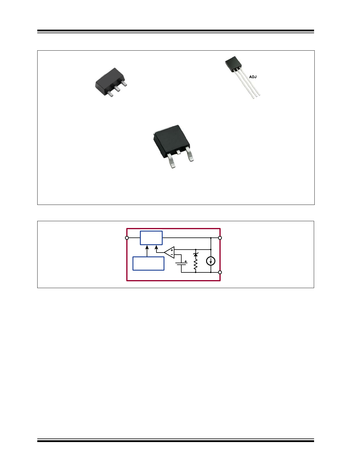
LR8
DS20005399B-page 2
2015-2017 Microchip Technology Inc.
Package Type
Functional Block Diagram
TO-92
See
Table 2-1
for pin information
TO-252
TO-243AA (SOT-89)
V
IN
ADJ
V
OUT
V
OUT
ADJ
9
,1
9
287
V
IN
ADJ
V
OUT
Overtemp &
Overcurrent
10μA
1.2V
V
IN
V
OUT
ADJ
LR8
Pass
Element
2015-2017 Microchip Technology Inc.
DS20005399B-page 3
LR8
1.0
ELECTRICAL CHARACTERISTICS
ABSOLUTE MAXIMUM RATINGS
†
V
IN
Input voltage (voltages ref to ADJ).............................................................................................................................. -0.5 to +480V
Output voltage range.......................................................................................................................................................... 0.5 to +470V
Operating ambient temperature range...........................................................................................................................–40°C to +85°C
Operating junction temperature range .........................................................................................................................–40°C to +125°C
Storage temperature ....................................................................................................................................................–65°C to +150°C
† Notice: Stresses above those listed under “Maximum Ratings” may cause permanent damage to the device. This is
a stress rating only and functional operation of the device at those or any other conditions above those indicated in the
operational listings of this specification is not implied. Exposure to maximum rating conditions for extended periods
may affect device reliability.
LR8
DS20005399B-page 4
2015-2017 Microchip Technology Inc.
ELECTRICAL CHARACTERISTICS
1
1
Test Conditions unless otherwise specified: -40°C <T
A
< 85°C.
Parameter
Sym.
Min.
Typ.
Max.
Units Conditions
Input to output voltage difference
V
IN
- V
OUT
12
450
V
Overall output voltage regulation
V
OUT
1.14
1.20
1.26
V
13.2V < V
IN
< 400V,
R
1
= 2.4 kΩ, R
2
= 0
375
400
425
V
R
1
= 2.4 kΩ, R
2
= 782 kΩ
Line regulation
∆V
OUT
0.003
0.01
%/V
17V < V
IN
< 400V, V
OUT
= 5V,
I
OUT
= 0.5mA
Load regulation
1.4
3.0
%
V
IN
= 17V, V
OUT
= 5V,
0.5 mA < I
OUT
< 10 mA
Temperature regulation
-1
+1
%
V
IN
= 17V, V
OUT
= 5V,
I
OUT
= 10 mA, -40°C < T
A
< 85°C
Output current limit
I
OUT
10
30
mA
T
J
< 85°C, V
IN
- V
OUT
= 12V
0.5
mA
T
J
> 125°C, V
IN
- V
OUT
= 450V
Minimum output current
I
OUT
0.3
0.5
mA
Includes R
1
and load current
Adjust output current
I
ADJ
5.0
10
15
µA
Minimum output load capacitance
C
LOAD
1.0
µF
Ripple rejection ratio
∆V
OUT
/∆V
IN
50
60
dB
120 Hz, V
OUT
= 5V
Junction temperature limit
T
LIMIT
125
°C
TABLE 1-1:
TYPICAL THERMAL RESISTANCE
Package
θ
ja
TO-252 (D-PAK)
81°C/W
TO-92
132°C/W
TO-243AA (SOT-89)
133°C/W
TABLE 1-2:
THERMAL CHARACTERISTICS
Package
Power Dissipation
@T
A
= 2.5°C
θ
jc
°C/W
θ
ja
°C/W
TO-92
0.74W
125
170
TO-243AA (SOT-89)
1.6W
15
78
1
1
Mounted on FR4 board, 25 mm x 2 mm x 1.57 mm
TO-252 (D-PAK)
2.5W
6.25
50
1
2015-2017 Microchip Technology Inc.
DS20005399B-page 5
LR8
2.0
PIN DESCRIPTION
The locations of the pins are listed in
Package Type
.
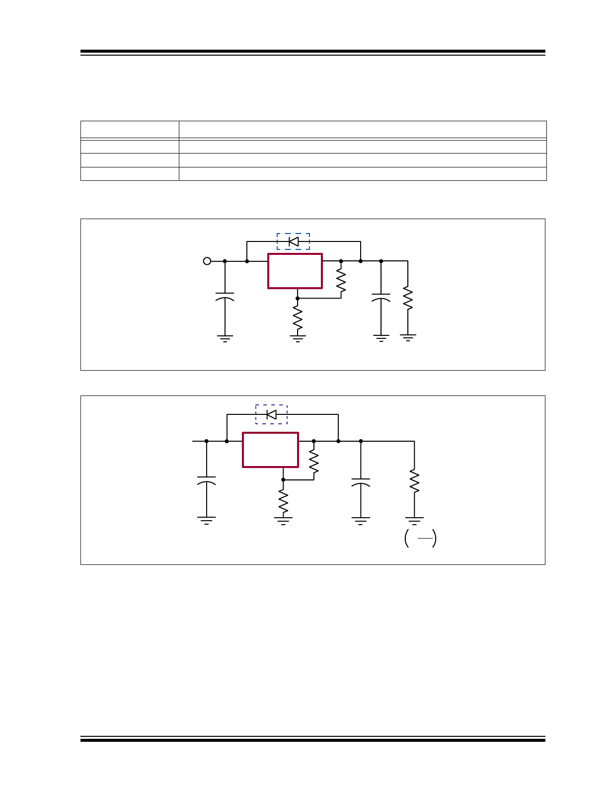
3.0
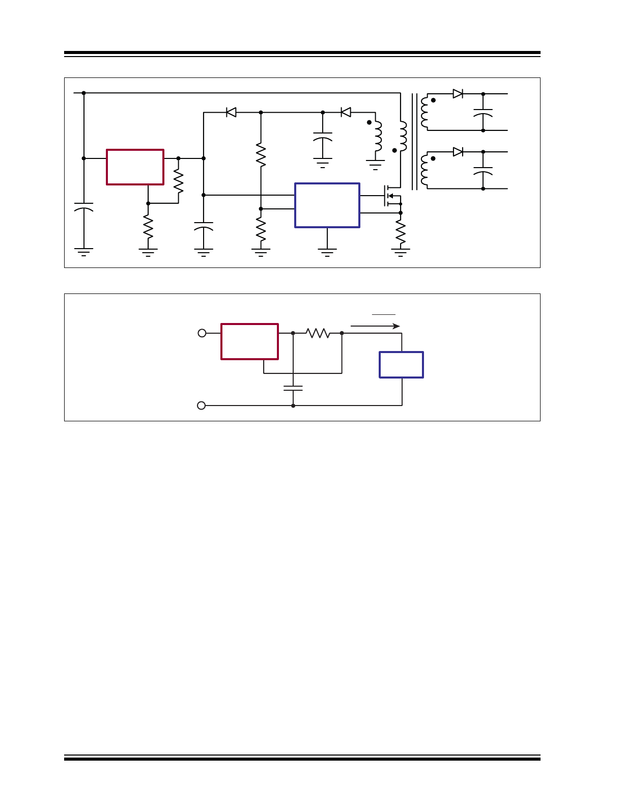
TYPICAL APPLICATION CIRCUITS
FIGURE 3-1:
Typical Application Circuit.
FIGURE 3-2:
High-input Voltage, 5.0V Output Linear Regulator.
TABLE 2-1:
PIN DESCRIPTION
Function
Description
V
IN
Regulator input. 13.2-450V.
V
OUT
Regulator output.
ADJ
Output voltage adjust.
LR8
V
IN
*
* Required for conditions where V
IN
is less than V
OUT
.
R
1
R
2
C
2
C
1
R
LOAD
V
OUT
V
OUT
ADJ
V
IN
V
IN
=
17 to 450V
*
R
1
6.04kΩ
1%
C
2
1.0μF
C
1
R
LOAD
≤16.5kΩ
V
OUT
= 5.0V
R
2
18.2kΩ
1%
* Required for conditions where V
IN
is less than V
OUT
V
OUT
= 1.20V 1+
R
2
+ ,
$'-
[5
R
1
LR8
V
OUT
ADJ
V
IN
LR8
DS20005399B-page 6
2015-2017 Microchip Technology Inc.
FIGURE 3-3:
SMPS Start-Up Circuit.
FIGURE 3-4:
High-voltage, Adjustable, Constant-Current Source.
+
V
OUT
1
-
V
CC
V
AUXILIARY
V
IN
= (V
OUT
+ 12V) to 450V
FB
PWM IC
+
V
OUT
1
-
LR8
V
OUT
ADJ
V
IN
LR8
V
IN
=
(V
OUT
+ 12V) to 450V
R
Load
I
OUT
=
1.20V
R
+
-
1.0μF
V
OUT
ADJ
V
IN
2015-2017 Microchip Technology Inc.
DS20005399B-page 7
LR8
FIGURE 3-5:
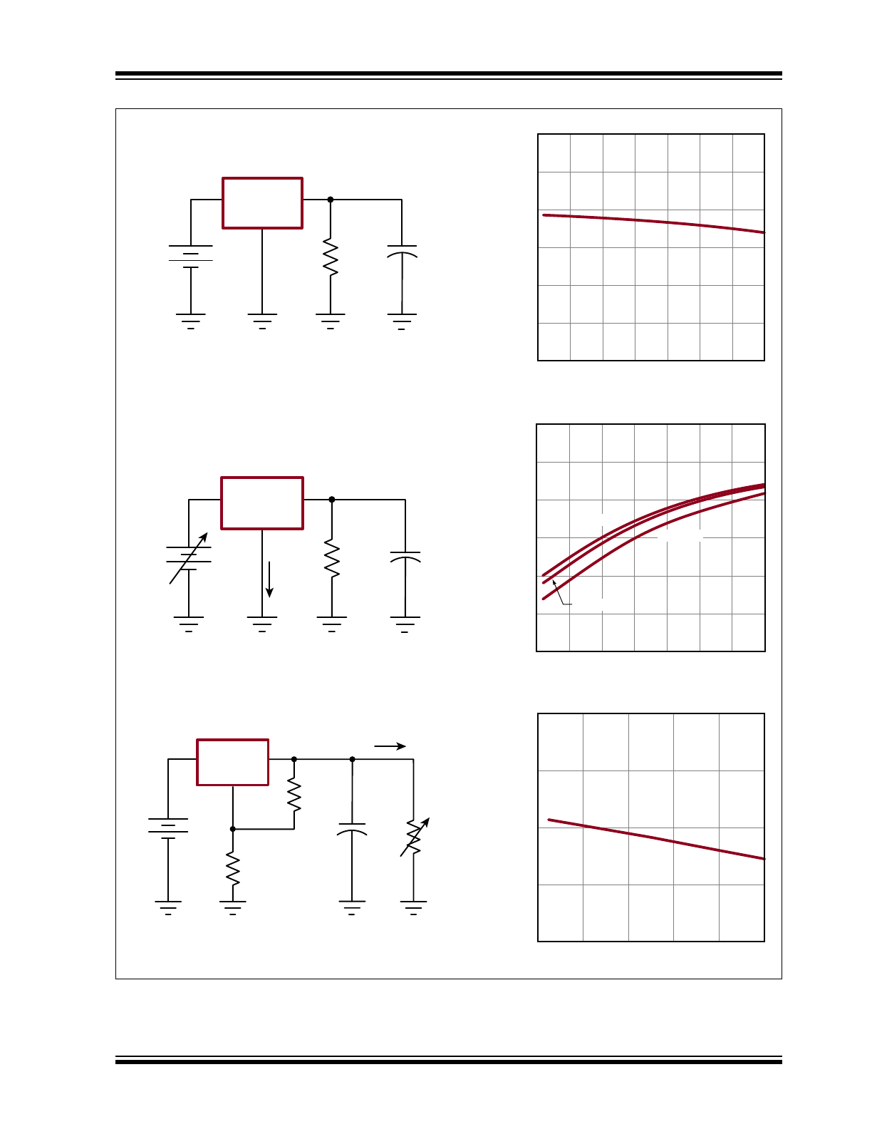
Typical Performance Curves 1 of 3.
12V
ADJ
V
IN
2.4k
Ω
1.0μF
V
OUT
= 1.2V
12V,
200V
400V
ADJ
V
IN
2.4kΩ
1.0ΩF
V
OUT = 1.2V
I
ADJ
V
OUT
(V)
T (junction) (
O
C)
Temperature Variation
-50 -25 0 25 50 75 100 125
1.00
1.05
1.10
1.15
1.20
1.25
1.30
Adjustment Current
I
ADJ
(μA)
T (junction) (
O
C)
-50 -25 0 25 50 75 100 125
6
7
8
9
10
11
12
V
IN
= 200V
V
OUT
(V)
I
OUT
(mA)
Load Regulation
0 2 4 6 8 10
4.8
4.9
5.0
5.1
5.2
ADJ
V
IN
6.04kΩ
±
1%
18.2kΩ
±
1%
1.0μF
R
LOAD
V
OUT
= 5.0V
25V
I
OUT
LR8
LR8
LR8
V
IN
= 400V
V
IN
= 12V
LR8
DS20005399B-page 8
2015-2017 Microchip Technology Inc.
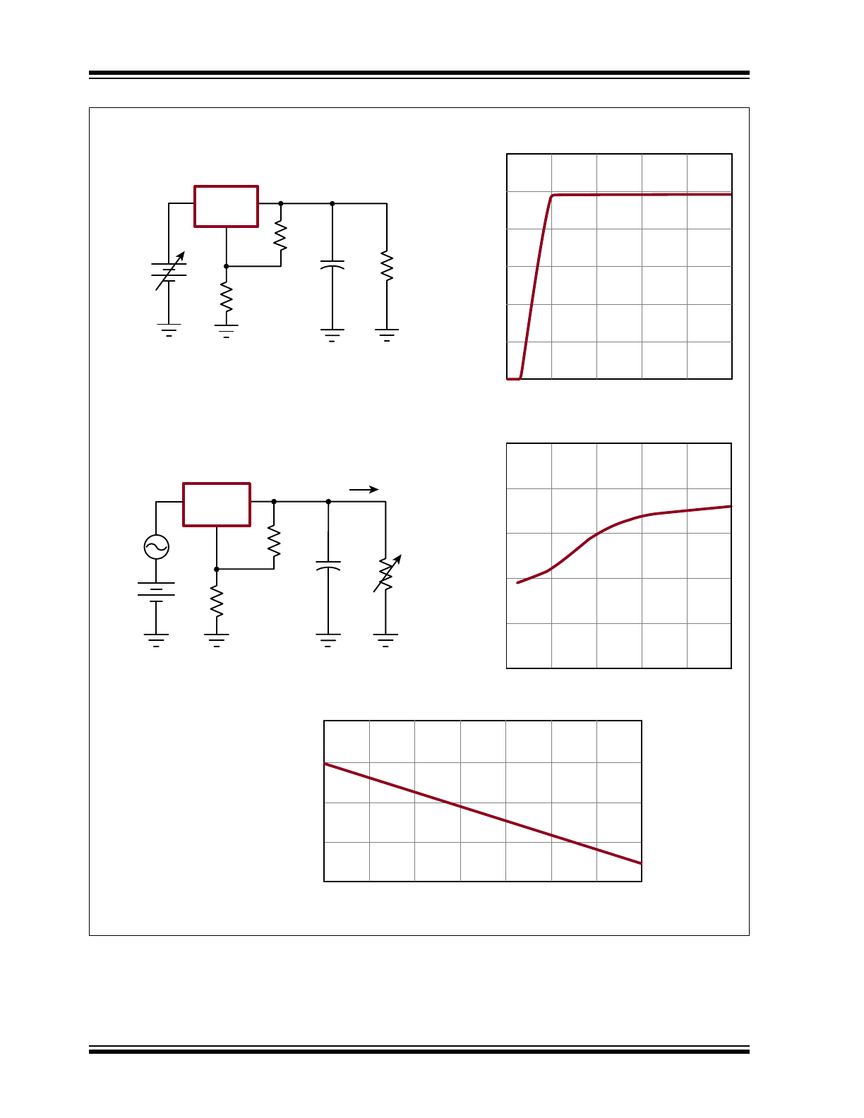
FIGURE 3-6:
Typical Performance Curves 2 of 3.
ADJ
V
IN
6.04kΩ
±1%
18.2kΩ
±1%
1.0μF
1kΩ
V
OUT
= 5.0V
0V to 50V
V
OUT
vs. V
IN
V
OUT
(V)
V
IN
(V)
0
10
20
30
40
50
0
1
2
3
4
5
6
Ripple Rejection
Ripple Regection Ratio (dB)
I
OUT
(mA)
0 2 4 6 8 10
-60
-61
-62
-63
-64
-65
ADJ
V
IN
6.04kΩ
±1%
18.2kΩ
±1%
1.0μF
R
LOAD
V
OUT
= 5.0V
65V
I
OUT
20V
P-P
@ 60Hz
30
25
20
15
10
-40 -20 0 20 40 60 80 100
Temperature (
O
C)
l
CL
(mA)
LR8
LR8
2015-2017 Microchip Technology Inc.
DS20005399B-page 9
LR8
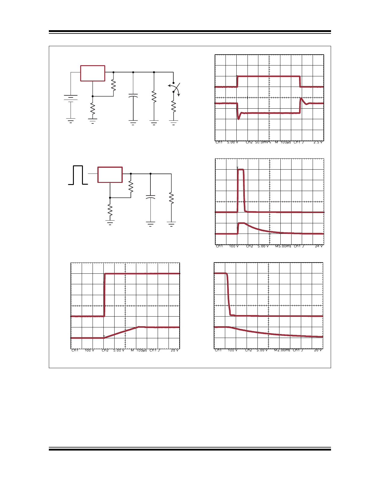
FIGURE 3-7:
Typical Performance Curves 3 of 3.
Load Transient Response
Line Transient Response
Line Power Up Transient
Load Transient Response
Line Transient Response
ADJ
V
IN
6.04kΩ
±1%
18.2kΩ
±1%
1.0μF
10kΩ
V
OUT
= 5.0V
25V
LR8
532Ω
sw
ADJ
V
IN
6.04kΩ
±1%
18.2kΩ
±1%
1.0μF
10kΩ
V
OUT
= 5.0V
LR8
400V
V
IN
0V
V
OUT
Closed
SW
Open
400V
V
IN
0V
V
OUT
0V
400V
V
IN
0V
5.0V
V
OUT
0V
400V
V
IN
0V
5.0V
V
OUT
0V
Line Power Down Transient
LR8
DS20005399B-page 10
2015-2017 Microchip Technology Inc.
4.0
PACKAGING INFORMATION
4.1
Package Marking Information
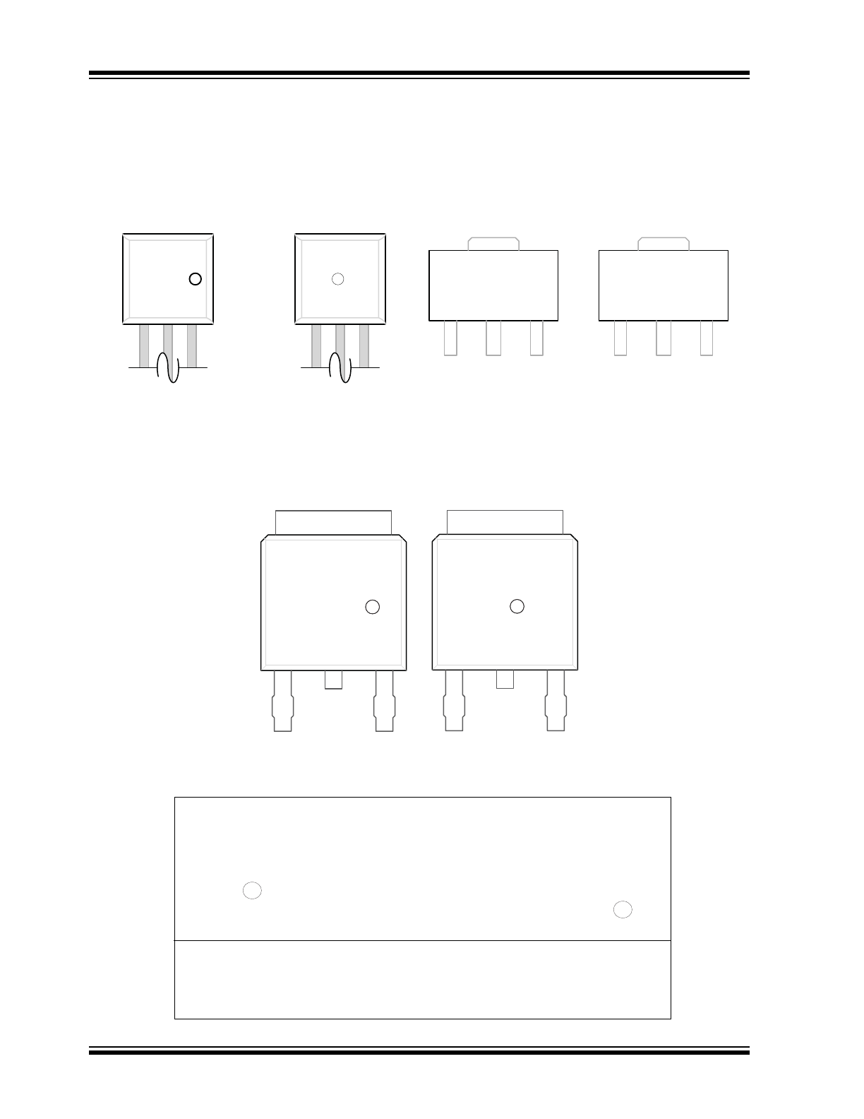
Legend: XX...X
Product Code or Customer-specific information
Y
Year code (last digit of calendar year)
YY
Year code (last 2 digits of calendar year)
WW
Week code (week of January 1 is week ‘01’)
NNN
Alphanumeric traceability code
Pb-free JEDEC
®
designator for Matte Tin (Sn)
*
This package is Pb-free. The Pb-free JEDEC designator ( )
can be found on the outer packaging for this package.
Note:
In the event the full Microchip part number cannot be marked on one line, it will
be carried over to the next line, thus limiting the number of available
characters for product code or customer-specific information. Package may or
not include the corporate logo.
3
e
3
e
3-lead TO-252
(D-PAK)
Example
YYWWNNN
XXXXX
XXXX
e3
1516343
8K4
LR
e3
3-lead TO-92
YWWNNN
XXXXXX
XXXX
e3
Example
516343
LR8
N3
e3
3-lead TO-243AA *
(SOT-89)
Example
XXXYYWW
NNN
LR8516
343