

2007-2017 Microchip Technology Inc.
DS00002516A-page 1
Highlights
• 3.3 Volt Operation (5 Volt Tolerant)
• LPC Interface
• ACPI 1.0 Compliant
• Fan Control
- Fan Speed Control Outputs
- Fan Tachometer Inputs
• Programmable Wake-up Event Interface
• PC98, PC99 Compliant
• Dual Game Port Interface
• MPU-401 MIDI Support
• General Purpose Input/Output Pins
• ISA Plug-and-Play Compatible Register Set
• Intelligent Auto Power Management
• System Management Interrupt
• 2.88MB Super I/O Floppy Disk Controller
- Licensed CMOS 765B Floppy Disk Controller
- Software and Register Compatible with
Microchip's Proprietary 82077AA Compatible
Core
- Supports Two Floppy Drives Directly
- Configurable Open Drain/Push-Pull Output
Drivers
- Supports Vertical Recording Format
- 16-Byte Data FIFO
- 100% IBM Compatibility
- Detects All Overrun and Under-run Condi-
tions
- Sophisticated Power Control Circuitry (PCC)
Including Multiple Powerdown Modes for
Reduced Power Consumption
- DMA Enable Logic
- Data Rate and Drive Control Registers
- 480 Address, Up to Eight IRQ and Three
DMA Options
• Enhanced Digital Data Separator
- 2 Mbps, 1 Mbps, 500 Kbps, 300 Kbps, 250
Kbps Data Rates
- Programmable Precompensation Modes
• Keyboard Controller
- 8042 Software Compatible
- 8 Bit Microcomputer
- 2k Bytes of Program ROM
- 256 Bytes of Data RAM
- Four Open Drain Outputs Dedicated for Key-
board/Mouse Interface
- Asynchronous Access to Two Data Registers
and One Status Register
- Supports Interrupt and Polling Access
- 8 Bit Counter Timer
- Port 92 Support
- Fast Gate A20 and KRESET Outputs
• Serial Ports
- Two Full Function Serial Ports
- High Speed NS16C550 Compatible UARTs
with Send/Receive 16-Byte FIFOs
- Supports 230k and 460k Baud
- Programmable Baud Rate Generator
- Modem Control Circuitry
- 480 Address and 15 IRQ Options
• Infrared Port
- Multi-protocol Infrared Interface
- IrDA 1.0 Compliant
- SHARP ASK IR
- 480 Addresses, Up to 15 IRQ
• Multi-Mode Parallel Port with ChiProtect
- Standard Mode IBM PC/XT, PC/AT, and PS/2
Compatible Bidirectional Parallel Port
- Enhanced Parallel Port (EPP) Compatible -
EPP 1.7 and EPP 1.9 (IEEE 1284 Compliant)
- IEEE 1284 Compliant Enhanced Capabilities
Port (ECP)
- ChiProtect Circuitry for Protection
- 480 Address, Up to 15 IRQ and Three DMA
Options
• LPC Interface
- Multiplexed Command, Address and Data
Bus
- Serial IRQ Interface Compatible with Serial-
ized IRQ Support for PCI Systems
- PME Interface
• 100-Pin QFP RoHS compliant package in a
3.2mm format
LPC47M112
Enhanced Super I/O Controller with LPC Interface

LPC47M112
DS00002516A-page 2
2007-2017 Microchip Technology Inc.
TO OUR VALUED CUSTOMERS
It is our intention to provide our valued customers with the best documentation possible to ensure successful use of your Microchip
products. To this end, we will continue to improve our publications to better suit your needs. Our publications will be refined and
enhanced as new volumes and updates are introduced.
If you have any questions or comments regarding this publication, please contact the Marketing Communications Department via
E-mail at
docerrors@microchip.com
. We welcome your feedback.
Most Current Data Sheet
To obtain the most up-to-date version of this data sheet, please register at our Worldwide Web site at:
http://www.microchip.com
You can determine the version of a data sheet by examining its literature number found on the bottom outside corner of any page.
The last character of the literature number is the version number, (e.g., DS30000000A is version A of document DS30000000).
Errata
An errata sheet, describing minor operational differences from the data sheet and recommended workarounds, may exist for cur-
rent devices. As device/documentation issues become known to us, we will publish an errata sheet. The errata will specify the
revision of silicon and revision of document to which it applies.
To determine if an errata sheet exists for a particular device, please check with one of the following:
• Microchip’s Worldwide Web site;
http://www.microchip.com
• Your local Microchip sales office (see last page)
When contacting a sales office, please specify which device, revision of silicon and data sheet (include -literature number) you are
using.
Customer Notification System
Register on our web site at
www.microchip.com
to receive the most current information on all of our products.

2007-2017 Microchip Technology Inc.
DS00002516A-page 3
LPC47M112
Table of Contents
1.0 General Description ........................................................................................................................................................................ 4
2.0 Pin Configuration ............................................................................................................................................................................ 6
3.0 3 Volt Operation / 5 Volt Tolerance ............................................................................................................................................... 12
4.0 Power Functionality ....................................................................................................................................................................... 13
5.0 Functional Description .................................................................................................................................................................. 16
6.0 Floppy Disk Controller ................................................................................................................................................................... 20
7.0 Command Set/Descriptions .......................................................................................................................................................... 37
8.0 Serial Port ..................................................................................................................................................................................... 56
9.0 Infrared Interface ........................................................................................................................................................................... 68
10.0 MPU-401 MIDI UART ................................................................................................................................................................. 69
11.0 Parallel Port ................................................................................................................................................................................ 74
12.0 Power Management .................................................................................................................................................................... 93
13.0 8042 Keyboard Controller Description ........................................................................................................................................ 99
14.0 General Purpose I/O ................................................................................................................................................................. 107
15.0 System Management Interrupt (SMI) ........................................................................................................................................ 113
16.0 PME Support ............................................................................................................................................................................. 114
17.0 Fan Speed Control and Monitoring ........................................................................................................................................... 117
18.0 Security Feature ........................................................................................................................................................................ 121
19.0 Game Port Logic ....................................................................................................................................................................... 122
20.0 Runtime Registers .................................................................................................................................................................... 125
21.0 Configuration ............................................................................................................................................................................. 150
22.0 Operational Description ............................................................................................................................................................ 168
23.0 Timing Diagrams ....................................................................................................................................................................... 172
24.0 Package Outline ........................................................................................................................................................................ 191
Appendix A: Test Mode ..................................................................................................................................................................... 192
Appendix B: Data Sheet Revision History ......................................................................................................................................... 195
LPC47M112
DS00002516A-page 4
2007-2017 Microchip Technology Inc.
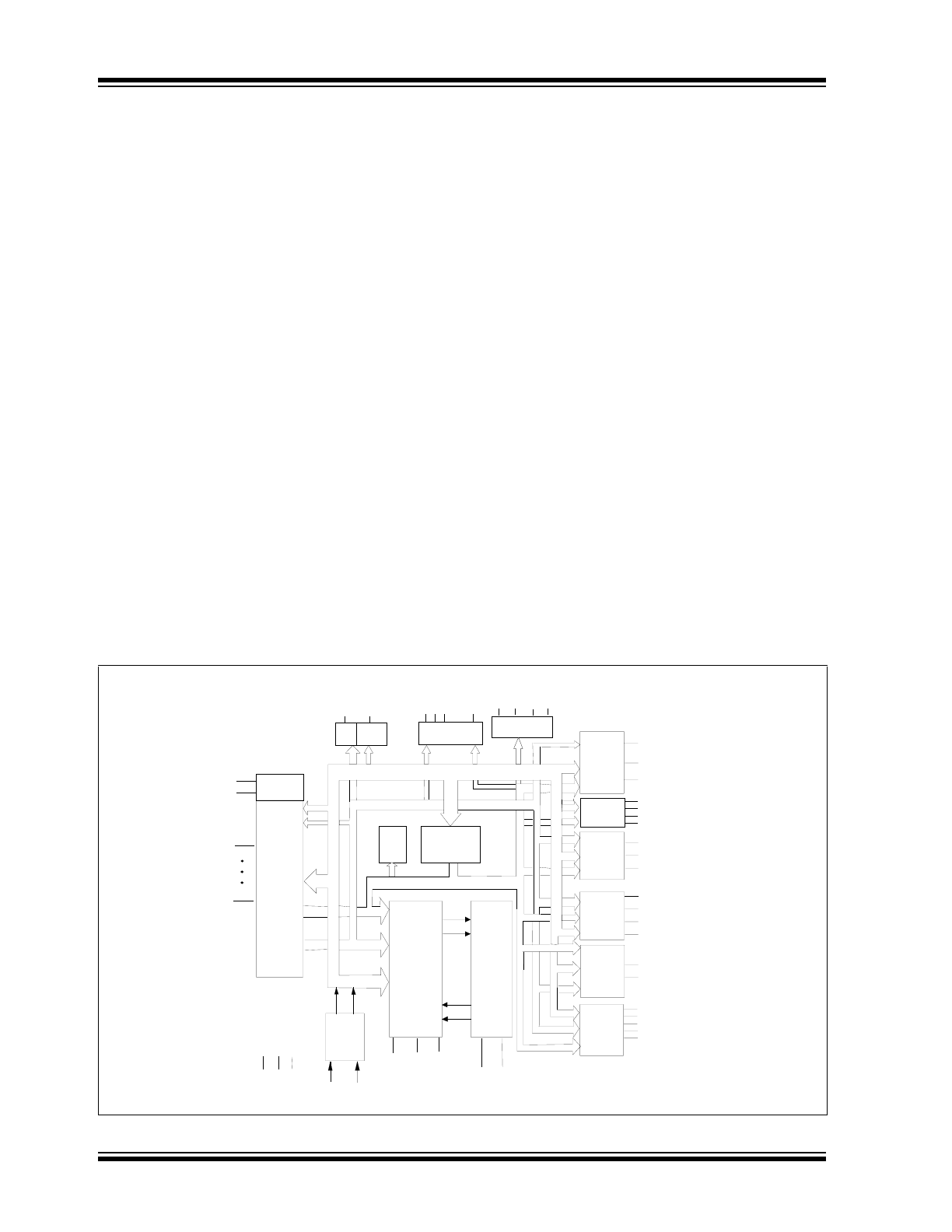
1.0
GENERAL DESCRIPTION
The LPC47M112 is a 3.3V (5V tolerant) PC98/PC99 compliant Super I/O controller. The LPC47M112 implements the
LPC interface, a pin reduced ISA bus interface which provides the same or better performance as the ISA/X-bus with a
substantial savings in pins used. The LPC47M112 provides fan control through two fan speed control output pins and
two fan tachometer input pins. It also provides 37 general purpose input/output (GPIO) pins, a dual game port interface
and MPU-401 MIDI support.
The LPC47M112 incorporates a keyboard interface, Microchip's true CMOS 765B floppy disk controller, advanced dig-
ital data separator, two 16C550A compatible UARTs, one Multi-Mode parallel port which includes ChiProtect circuitry
plus EPP and ECP, on-chip 12 mA AT bus drivers, one floppy direct drive support, and Intelligent Power Management
including PME support. The true CMOS 765B core provides 100% compatibility with IBM PC/XT and PC/AT architec-
tures in addition to providing data overflow and underflow protection. The Microchip advanced digital data separator
incorporates Microchip's patented data separator technology, allowing for ease of testing and use. Both on-chip UARTs
are compatible with the NS16C550A. The parallel port is compatible with IBM PC/AT architecture, as well as IEEE 1284
EPP and ECP. The LPC47M112 incorporates sophisticated power control circuitry (PCC) which includes support for
keyboard and mouse wake-up events. The PCC supports multiple low power-down modes.
The LPC47M112 supports the ISA Plug-and-Play Standard (Version 1.0a) and provides the recommended functionality
to support Windows '95, Windows 98, Windows 2000 and Windows ME.
The I/O Address, DMA Channel and hardware IRQ of each logical device in the LPC47M112 may be reprogrammed
through the internal configuration registers. There are 480 I/O address location options, a Serialized IRQ interface, and
three DMA channels.
The LPC47M112 does not require any external filter components and is therefore easy to use and offers lower system
costs and reduced board area. The LPC47M112 is software and register compatible with Microchip's proprietary
82077AA core.
1.1
Block Diagram
FIGURE 1-1:
LPC47M112 BLOCK DIAGRAM
CLOCK
GEN
CLOCKI
14MHz
nINDEX
nTRK0
nDSKCHG
nWRPRT
nWGATE
DENSEL
nDIR
nSTEP
nHDSEL
nDS0
nMTR0
RDATA
RCLOCK
nWDATA
SMSC
PROPRIETARY
82077
COMPATIBLE
VERTICAL
FLOPPYDISK
CONTROLLER
CORE
DIGITAL
DATA
SEPARATOR
WITH WRITE
PRECOM-
PENSATION
DRVDEN0
DRVDEN1
*
Vcc Vss
CLK32
32KHz
V
TR
nRDATA
nDSR2, nDCD2, nRI2, nDTR2
*
8042
KCLK
KDATA
MCLK
MDATA
GATEA20, KRESET
*
Denotes Multifunction Pins
MPU-401
SERIAL
PORT
MIDI_IN
MIDI_OUT
nDSR1, nDCD1, nRI1, nDTR1
TXD1, nCTS1, nRTS1
nINIT, nALF
MULTI-MODE
PARALLEL
PORT
MUX
16C550
COMPATIBLE
SERIAL
PORT 1
16C550
COMPATIBLE
SERIAL
PORT 2 WITH
INFRARED
DATA BUS
WDATA
WCLOCK
TXD2(IRTX), nCTS2, nRTS2
*
RXD2(IRRX)
*
RXD1
PD0-7
BUSY, SLCT, PE,
nERROR, nACK
nSTB, nSLCTIN,
IRRX2, IRTX2
CONFIGURATION
REGISTERS
CONTROL BUS
Fan
Control
FAN1*
FAN2*
FAN_TACH1*
FAN_TACH2*
GENERAL
PURPOSE
I/O
GP1[0:7]*
GP2[0:2,4:7]*
Game Port
...
Game Port Signals*
(1-Dual)
GP3[0:7]*, GP4[0:3]*
GP5[0:7]*, GP6[0:1]*
LPC BUS
INTERFACE
ADDRESS BUS
SERIAL
IRQ
SER_IRQ
PCI_CLK
LPC Bus
Signals
ACPI
BLOCK
PME
nIO_PME
SMI
nIO_SMI

2007-2017 Microchip Technology Inc.
DS00002516A-page 5
LPC47M112
1.2
Reference Documents
1.
Microchip Consumer Infrared Communications Controller (CIrCC) V1.X
2.
IEEE 1284 Extended Capabilities Port Protocol and ISA Standard, Rev. 1.14, July 14, 1993
3.
Hardware Description of the 8042, Intel 8 bit Embedded Controller Handbook
4.
PCI Bus Power Management Interface Specification, Rev. 1.0, Draft, March 18, 1997
5.
Low Pin Count (LPC) Interface Specification, Revision 1.0, September 29, 1997, Intel Document
LPC47M112
DS00002516A-page 6
2007-2017 Microchip Technology Inc.
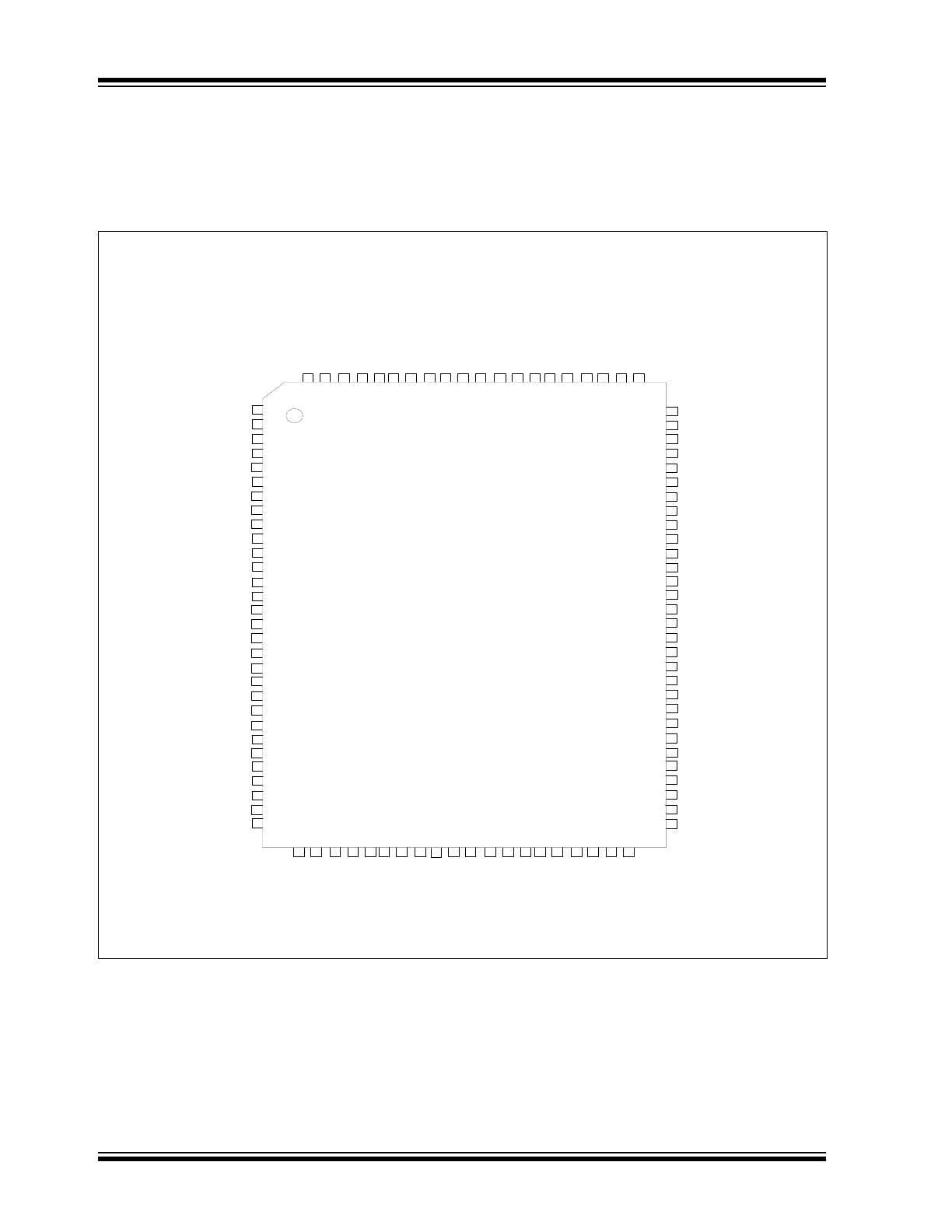
2.0
PIN CONFIGURATION
2.1
Pin Diagram
FIGURE 2-1:
LPC47M112 PIN DIAGRAM
LP C 4 7 M 1 0 x
1 0 0 P IN Q F P
G P 4 0/D RV D E N 0
G P 4 1/D RV D E N 1
nM TR 0
nD S K C H G
nD S 0
C LK I32
V S S
n D IR
nS TE P
nW DATA
nW G ATE
nH D S E L
nIN D E X
nTR K 0
nW RTP RT
nR DATA
G P 42 /nIO _P M E
V T R
C LO C K I
LA D 0
LA D 1
LA D 2
LA D 3
nLF R A M E
nL D R Q
nP C I_R E S E T
nLP C P D
G P 43/D D R C
P C I_ C LK
SE R _IR Q
1
2
3
4
5
6
7
8
9
1 0
1 1
1 2
1 3
1 4
1 5
1 6
1 7
1 8
1 9
2 0
2 1
2 2
2 3
2 4
2 5
2 6
2 7
2 8
2 9
3 0
nAC K
BU S Y
PE
SLC T
VS S
PD 7
PD 6
PD 5
PD 4
PD 3
PD 2
PD 1
PD 0
nS LC T IN
nIN IT
VC C
G P 37/A 20M
G P 36/nKB D R S T
IRTX 2/G P35
IR R X 2/G P 34
VS S
M C LK
M DAT
KC LK
KDAT
G P 33/FAN 1
G P 32/FAN 2
VC C
G P 31/FAN _TAC H 1
G P 30/FA N _TAC H 2
80
79
78
77
76
75
74
73
72
71
70
69
68
67
66
65
64
63
62
61
60
59
58
57
56
55
54
53
52
51
VSS
GP10/
J1B1
GP11
/J
1B
2
GP
12/
J2B1
GP13
/J
2B
2
G
P
14/J
1X
G
P
15
/J
1Y
GP
16
/J2X
G
P
17/
J2
Y
AV
S
S
GP20
/P
17
G
P
21
/P
16
/n
D
S
1
G
P
22/P12
/nM
TR
1
VR
EF
GP24/
SYSOPT
GP25/
M
ID
I_IN
G
P
26/M
ID
I_OU
T
GP60/
LED
1
GP61/
LE
D
2
G
P
27
/nIO_
SM
I
31
32
33
34
35
36
37
38
39
40
41
42
43
44
45
46
47
48
49
50
GP5
7/nDTR2
GP5
6/n
CTS2
GP5
5/nR
TS2
G
P
54/n
DS
R2
GP53
/TXD2(
IR
TX
)
G
P
52/RX
D2(
IRRX
)
G
P
51
/n
DCD2
VC
C
GP5
0/
nRI2
nD
CD1
nRI1
nD
TR1
nCT
S1
nR
TS
1
nDSR1
TX
D
1
RX
D1
nST
R
OBE
nALF
nERR
O
R
10
0
99
98
97
9
6
95
9
4
93
92
91
90
89
88
87
86
85
84
83
82
8
1
LPC47M112
2007-2017 Microchip Technology Inc.
DS00002516A-page 7
LPC47M112
2.2
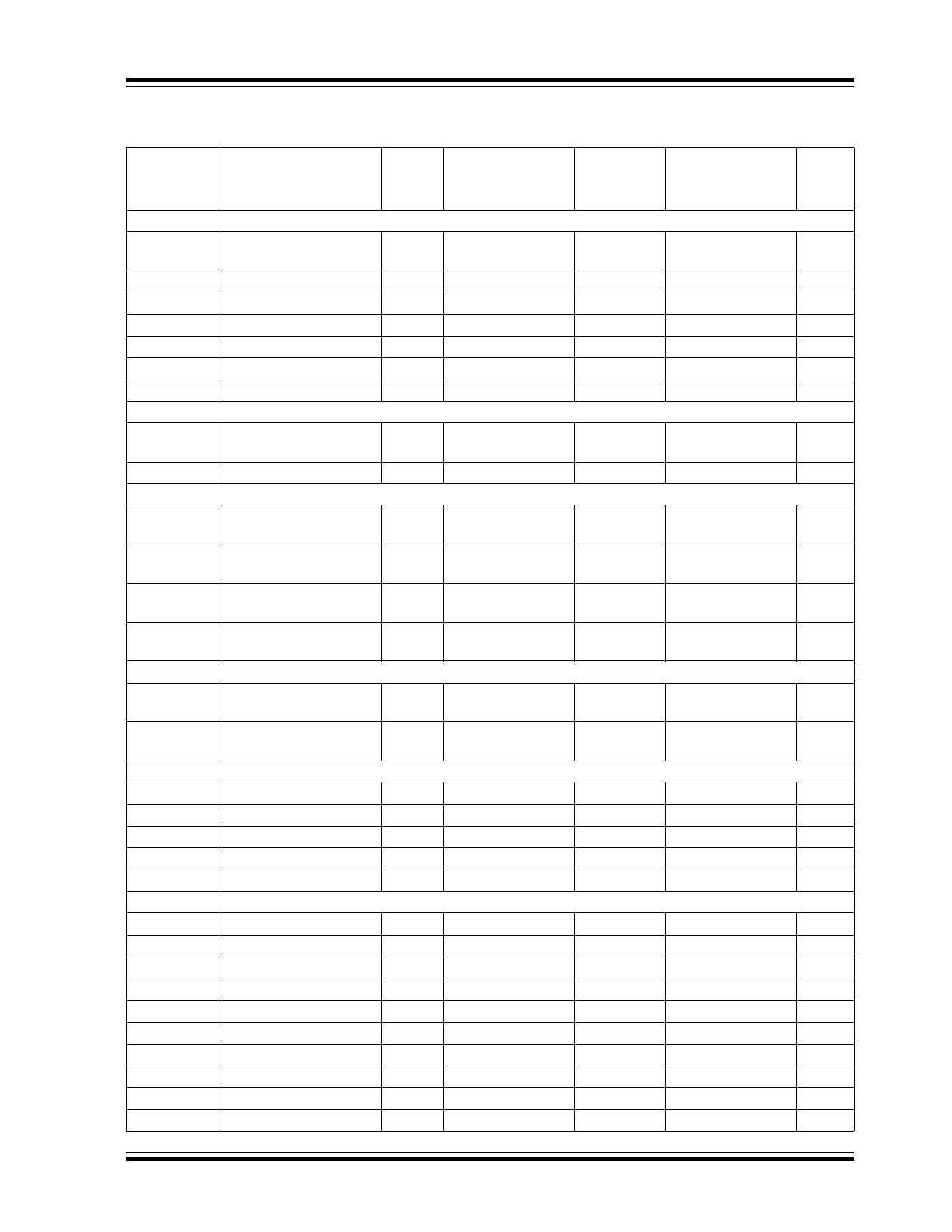
Description of Pin Functions
Pin No./
QFP
Name
Total
Symbol
Buffer Type
Buffer Type per
Function
(
Note 1
)
Notes
PROCESSOR/HOST LPC INTERFACE (10)
23:20
Multiplexed Command,
Address, Data [3:0]
4
LAD[3:0]
PCI_IO
PCI_IO
24
Frame
1
nLFRAME
PCI_I
PCI_I
25
Encoded DMA Request
1
nLDRQ
PCI_O
PCI_O
26
PCI Reset
1
nPCI_RESET
PCI_I
PCI_I
27
Power Down
1
nLPCPD
PCI_I
PCI_I
2
29
PCI Clock
1
PCI_CLK
PCI_ICLK
PCI_ICLK
30
Serial IRQ
1
SER_IRQ
PCI_IO
PCI_IO
CLOCKS (2)
6
32.768 Trickle Clock
Input
1
CLOCKI32
IS
IS
3
19
14.318MHz Clock Input
1
CLOCKI
IS
IS
FAN CONTROL (4)
51
General Purpose I/O
/Fan Tachometer 2
1
GP30/
FAN_TACH2
IO8
(I/O8/OD8)/I
52
General Purpose I/O
/Fan Tachometer 1
1
GP31/
FAN_TACH1
IO8
(I/O8/OD8)/I
54
General Purpose I/O
/Fan Speed Control 2
1
GP32/FAN2
IO12
(I/O12/OD12)/
(O12/OD12)
4
55
General Purpose I/O
/Fan Speed Control 1
1
GP33/FAN1
IO12
(I/O12/OD12)/
(O12/OD12)
4
INFRARED INTERFACE (2)
61
Infrared Rx
/General Purpose I/O
1
IRRX2/GP34
IS/O8
IS/(IS/O8/OD8)
62
Infrared Tx
/General Purpose I/O
1
IRTX2/GP35
IO12
O12/(I/O12/ OD12)
5
,
6
POWER PINS (10)
53, 65,93
Power
3
VCC
7, 31, 60,76
Ground
4
VSS
40
Analog Ground
1
AVSS
44
Reference Voltage
1
VREF
18
Trickle Voltage
1
VTR
7
FDD INTERFACE (14)
16
Read Disk Data
1
nRDATA
IS
IS
11
Write Gate
1
nWGATE
O12
(O12/OD12)
10
Write Disk Data
1
nWDATA
O12
(O12/OD12)
12
Head Select
1
nHDSEL
O12
(O12/OD12)
8
Step Direction
1
nDIR
O12
(O12/OD12)
9
Step Pulse
1
nSTEP
O12
(O12/OD12)
4
Disk Change
1
nDSKCHG
IS
IS
5
Drive Select 0
1
nDS0
O12
(O12/OD12)
3
Motor On 0
1
nMTR0
O12
(O12/OD12)
15
Write Protected
1
nWRTPRT
IS
IS
LPC47M112
DS00002516A-page 8
2007-2017 Microchip Technology Inc.
14
Track 0
1
nTRKO
IS
IS
13
Index Pulse Input
1
nINDEX
IS
IS
1
General Purpose I/O/
Drive Density Select 0
1
GP40/DRVDEN0
IO12
(I/O12/OD12)/
(O12/OD12)
2
General Purpose I/O/
Drive Density Select 1
1
GP41/DRVDEN1
IO12
(I/O12/OD12)/
(O12/OD12)
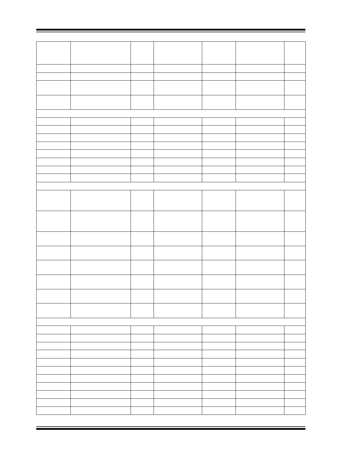
SERIAL PORT 1 INTERFACE (8)
84
Receive Serial Data 1
1
RXD1
IS
IS
85
Transmit Serial Data 1
1
TXD1
O12
O12
87
Request to Send 1
1
nRTS1/SYSOP
O8
O8
88
Clear to Send 1
1
nCTS1
I
I
89
Data Terminal Ready 1
1
nDTR1
O6
O6
86
Data Set Ready 1
1
nDSR1
I
I
91
Data Carrier Detect 1
1
nDCD1
I
I
90
Ring Indicator 1
1
nRI1
I
I
SERIAL PORT 2 INTERFACE (8)
95
General Purpose I/O
/Receive Serial Data 2
(Infrared Rx)
1
GP52/RXD2(IRRX) IS/O8
(IS/O8/OD8)
/IS
96
General Purpose I/O
/Transmit Serial Data 2
(Infrared Tx)
1
GP53/TXD2(IRTX) IO12
(I/O12/
OD12)/O12
5
98
General Purpose I/O
/Request to Send 2
1
GP55/nRTS2
IO8
(I/O8/OD8)/O8
99
General Purpose I/O
/Clear to Send 2
1
GP56/
nCTS2
IO8
(I/O8/OD8)/I
100
General Purpose I/O
/Data Terminal Ready
1
GP57/
nDTR2
IO8
(I/O8/OD8)/O8
97
General Purpose I/O
/Data Set Ready 2
1
GP54/
nDSR2
IO8
(I/O8/OD8)/I
94
General Purpose I/O/
Data Carrier Detect 2
1
GP51/nDCD2 IO8
(I/O8/OD8)/I
92
General Purpose I/O/
Ring Indicator 2
1
GP50/nRI2
IO8
(I/O8/OD8)/I
PARALLEL PORT INTERFACE (17)
66
Initiate Output
1
nINIT
OP14
(OD14/OP14)
67
Printer Select Input
1
nSLCTIN
OP14
(OD14/OP14)
68
Port Data 0
1
PD0
IOP14
IOP14
69
Port Data 1
1
PD1
IOP14
IOP14
70
Port Data 2
1
PD2
IOP14
IOP14
71
Port Data 3
1
PD3
IOP14
IOP14
72
Port Data 4
1
PD4
IOP14
IOP14
73
Port Data 5
1
PD5
IOP14
IOP14
74
Port Data 6
1
PD6
IOP14
IOP14
75
Port Data 7
1
PD7
IOP14
IOP14
77
Printer Selected Status
1
SLCT
IO12
I/OD12
Pin No./
QFP
Name
Total
Symbol
Buffer Type
Buffer Type per
Function
(
Note 1
)
Notes
2007-2017 Microchip Technology Inc.
DS00002516A-page 9
LPC47M112
78
Paper End
1
PE
I
I
79
Busy
1
BUSY I
I
80
Acknowledge
1
nACK I
I
81
Error
1
nERROR I
I
82
Auto-feed Output
1
nALF
OP14
(OD14/OP14)
83
Strobe Output
1
nSTROBE
OP14
(OD14/OP14)
KEYBOARD/MOUSE INTERFACE (6)
56
Keyboard Data
1
KDAT
IOD16
IOD16
57
Keyboard Clock
1
KCLK
IOD16
IOD16
58
Mouse Data
1
MDAT
IOD16
IOD16
59
Mouse Clock
1
MCLK
IOD16
IOD16
63
General Purpose I/O
/Keyboard Reset
1
GP36/nKBDRST IO8
(I/O8/OD8)/O8
9
64
General Purpose I/O
/Gate A20
1
GP37/A20M
IO8
(I/O8/OD8)/O8
9
GENERAL PURPOSE I/O (19)
32
General Purpose I/O/
Joystick 1 Button 1
1
GP10/J1B1
IS/O8
(IS/O8/OD8)/IS
33
General Purpose I/O/
Joystick 1 Button 2
1
GP11/J1B2
IS/O8
(IS/O8/OD8)/IS
34
General Purpose I/O/
Joystick 2 Button 1
1
GP12/J2B1
IS/O8
(IS/O8/OD8)/IS
35
General Purpose I/O/
Joystick 2 Button 2
1
GP13/J2B2
IS/O8
(IS/O8/OD8)/IS
36
General Purpose I/O/
Joystick 1 X-Axis
1
GP14/J1X
IO12
(I/O12/ OD12)/
IO12
37
General Purpose I/O/
Joystick 1 Y-Axis
1
GP15/J1Y
IO12
(I/O12/ OD12)/
IO12
38
General Purpose I/O/
Joystick 2 X-Axis
1
GP16/J2X
IO12
(I/O12/OD12)/IO12
39
General Purpose I/O/
Joystick 2 Y-Axis
1
GP17/J2Y
IO12
(I/O12/OD12)/IO12
41
General Purpose I/O/
P17
1
GP20/P17
IO8
(I/O8/OD8)/IO8
42
General Purpose I/O/
P16 /nDS1
1
GP21/P16/nDS1
IO12
(I/O12/OD12)/
IO12/(O12/ OD12)
43
General Purpose I/O/
P12/nMTR1
1
GP22/P12 nMTR1
IO12
(I/O12/ OD12)/
IO12/ (O12/OD12)
45
General Purpose I/O/
System Option
1
GP24/SYSOPT
IO8
(I/O8/OD8)
8
46
General Purpose I/O/
MIDI_IN
1
GP25/MIDI_IN
IO8
(I/O8/OD8)/I
47
General Purpose I/O/
MIDI_OUT
1
GP26/MIDI_OUT
IO12
(I/O12/OD12)/O12
50
General Purpose I/O
/SMI Output
1
GP27/nIO_SMI
IO12
(I/O12/OD12)/
OD12
Pin No./
QFP
Name
Total
Symbol
Buffer Type
Buffer Type per
Function
(
Note 1
)
Notes
LPC47M112
DS00002516A-page 10
2007-2017 Microchip Technology Inc.
Note 1:
Buffer types per function on multiplexed pins are separated by a slash “/”. Buffer types in parenthesis repre-
sent multiple buffer types for a single pin function.
2:
The nLPCPD pin may be tied high. The LPC interface will function properly if the nPCI_RESET signal fol-
lows the protocol defined for the nLRESET signal in the “Low Pin Count Interface Specification”.
3:
If the 32kHz input clock is not used the CLKI32 pin must be grounded. There is a bit in the configuration reg-
ister at 0xF0 in Logical Device A that indicates whether or not the 32kHz clock is connected. This bit deter-
mines the clock source for the fan tachometer, LED and “wake on specific key” logic. Set this bit to ‘1’ if the
clock is not connected.
4:
The fan control pins (FAN1 and FAN2) come up as outputs and low following a VCC POR and Hard Reset.
These pins revert to their non-inverting GPIO output function when VCC is removed from the part.
5:
The IRTX pins (IRTX2/GP35 and GP53/TXD2 (IRTX)) are driven low when the part is powered by VTR
(VCC=0V with VTR=3.3V). These pins will remain low following a power-up (VCC POR) until serial port 2 is
enabled by setting the activate bit, at which time the pin will reflect the state of the transmit output of the
Serial Port 2 block.
6:
The VCC power-up default for this pin is Logic “0” if the IRTX function is programmed on the GPIO.
7:
VTR can be connected to VCC if no wakeup functionality is required.
8:
The GP24 /SYSOPT pin requires an external pulldown resistor to put the base IO address for configuration
at 0x02E. An external pullup resistor is required to move the base IO address for configuration to 0x04E.
9:
External pullups must be placed on the nKBDRST and A20M pins. These pins are GPIOs that are inputs
after an initial power-up (VTR POR). If the nKBDRST and A20M functions are to be used, the system must
ensure that these pins are high. See
Section 2.4, "Pins That Require External Pullup Resistors"
.
10:
The LED pins are powered by VTR so that the LEDs can be controlled when the part is under VTR power.
2.3
Buffer Type Descriptions
IO12
Input/Output, 12mA sink, 6mA source.
IS/O12
Input with Schmitt Trigger/Output, 12mA sink, 6mA source.
O12
Output, 12mA sink, 6mA source.
OD12
Open Drain Output, 12mA sink.
O6
Output, 6mA sink, 3mA source.
O8
Output, 8mA sink, 4mA source.
OD14
Open Drain Output, 14mA sink.
OP14
Output, 14mA sink, 14mA source.
48
General Purpose I/O/
LED
1
GP60/LED1
IO12
(I/O12/OD12)/O12
10
49
General Purpose I/O/
LED
1
GP61/LED2
IO12
(I/O12/OD12)/O12
10
17
General Purpose I/O/
Power Management
Event
1
GP42/nIO_PME
IO12
(I/O12/OD12)/
OD12
28
General Purpose I/O
/Device Disable Reg.
Control
1
GP43/DDRC
IO8
(I/O8/OD8)/I
Note:
The "n" as the first letter of a signal name indicates an "Active Low" signal.
Note:
The buffer type values are specified at VCC=3.3V.
Pin No./
QFP
Name
Total
Symbol
Buffer Type
Buffer Type per
Function
(
Note 1
)
Notes