

2004-2017 Microchip Technology Inc.
DS00002492A-page 1
Highlights
• 3.3 Volt Operation, 5 Volt Tolerant
• LPC Interface
• Fan Control
- Fan Speed Control Outputs (2)
- Fan Tachometer Inputs (2)
• Programmable Wake-up Event Interface
• PC98, PC99, and ACPI 1.0 Compliant
• Dual Game Port Interface
• MPU-401 MIDI Support
• General Purpose Input/Output Pins (37)
• ISA IRQ to Serial IRQ Conversion
• ISA Plug-and-Play Compatible Register Set
• Intelligent Auto Power Management
• System Management Interrupt
• 2.88MB Super I/O Floppy Disk Controller
- Licensed CMOS 765B Floppy Disk Controller
- Software and Register Compatible with
Microchip’s Proprietary 82077AA Compatible
Core
- Supports Two Floppy Drives Directly
- Configurable Open Drain/Push-Pull Output
Drivers
- Supports Vertical Recording Format
- 16-Byte Data FIFO
- 100% IBM Compatibility
- Detects All Overrun and Underrun Conditions
- Sophisticated Power Control Circuitry (PCC)
Including Multiple Powerdown Modes for
Reduced Power Consumption
- DMA Enable Logic
- Data Rate and Drive Control Registers
- 480 Address, Up to 15 IRQ and Three DMA
Options
• Floppy Disk Available on Parallel Port Pins
• Enhanced Digital Data Separator
- 2 Mbps, 1 Mbps, 500 Kbps, 300 Kbps, 250
Kbps Data Rates
- Programmable Precompensation Modes
• Keyboard Controller
- 8042 Software Compatible
- 8 Bit Microcomputer
- 2k Bytes of Program ROM
- 256 Bytes of Data RAM
- Four Open Drain Outputs Dedicated for Key-
board/Mouse Interface
- Asynchronous Access to Two Data Registers
and One Status Register
- Supports Interrupt and Polling Access
- 8 Bit Counter Timer
- Port 92 Support
- Fast Gate A20 and KRESET Outputs
• Serial Ports
- Two Full Function Serial Ports
- High Speed NS16C550A Compatible UARTs
with Send/Receive 16-Byte FIFOs
- Supports 230k and 460k Baud
- Programmable Baud Rate Generator
- Modem Control Circuitry
- 480 Address and 15 IRQ Options
• Infrared Port
- Multiprotocol Infrared Interface
- 32-Byte Data FIFO
- IrDA 1.0 Compliant
- Consumer IR
- SHARP ASK IR
- 480 Address, Up to 15 IRQ and Three DMA
Options
• Multi-Mode Parallel Port with ChiProtect
- Standard Mode IBM PC/XT
,
PC/AT, and PS/2
Compatible Bidirectional Parallel Port
- Enhanced Parallel Port (EPP) Compatible -
EPP 1.7 and EPP 1.9 (IEEE 1284 Compliant)
- IEEE 1284 Compliant Enhanced Capabilities
Port (ECP)
- ChiProtect Circuitry for Protection
- 960 Address, Up to 15 IRQ and Three DMA
Options
• LPC Interface
- Multiplexed Command, Address and Data
Bus
- Serial IRQ Interface Compatible with Serial-
ized IRQ Support for PCI Systems
- PME Interface
• 100 Pin QFP RoHS Compliant Package
LPC47B27x
100 Pin Enhanced Super I/O Controller with LPC Interface

LPC47B27x
DS00002492A-page 2
2004-2017 Microchip Technology Inc.
TO OUR VALUED CUSTOMERS
It is our intention to provide our valued customers with the best documentation possible to ensure successful use of your Microchip
products. To this end, we will continue to improve our publications to better suit your needs. Our publications will be refined and
enhanced as new volumes and updates are introduced.
If you have any questions or comments regarding this publication, please contact the Marketing Communications Department via
E-mail at
docerrors@microchip.com
. We welcome your feedback.
Most Current Data Sheet
To obtain the most up-to-date version of this data sheet, please register at our Worldwide Web site at:
http://www.microchip.com
You can determine the version of a data sheet by examining its literature number found on the bottom outside corner of any page.
The last character of the literature number is the version number, (e.g., DS30000000A is version A of document DS30000000).
Errata
An errata sheet, describing minor operational differences from the data sheet and recommended workarounds, may exist for cur-
rent devices. As device/documentation issues become known to us, we will publish an errata sheet. The errata will specify the
revision of silicon and revision of document to which it applies.
To determine if an errata sheet exists for a particular device, please check with one of the following:
• Microchip’s Worldwide Web site;
http://www.microchip.com
• Your local Microchip sales office (see last page)
When contacting a sales office, please specify which device, revision of silicon and data sheet (include -literature number) you are
using.
Customer Notification System
Register on our web site at
www.microchip.com
to receive the most current information on all of our products.

2004-2017 Microchip Technology Inc.
DS00002492A-page 3
LPC47B27x
Table of Contents
1.0 General Description ........................................................................................................................................................................ 4
2.0 Pin Configuration ............................................................................................................................................................................ 7
3.0 Power Functionality ....................................................................................................................................................................... 14
4.0 Functional Description .................................................................................................................................................................. 18
5.0 Floppy Disk Controller ................................................................................................................................................................... 22
6.0 Command Set/Descriptions .......................................................................................................................................................... 37
7.0 Serial Port (UART) ........................................................................................................................................................................ 56
8.0 Infrared Interface ........................................................................................................................................................................... 68
9.0 MPU-401 MIDI UART ................................................................................................................................................................... 69
10.0 Parallel Port ................................................................................................................................................................................ 74
11.0 Power Management .................................................................................................................................................................... 94
12.0 Serial IRQ ................................................................................................................................................................................... 98
13.0 8042 Keyboard Controller Description ...................................................................................................................................... 101
14.0 General Purpose I/O ................................................................................................................................................................. 110
15.0 System Management Interrupt (SMI) ........................................................................................................................................ 117
16.0 PME Support ............................................................................................................................................................................. 118
17.0 Fan Speed Control and Monitoring ........................................................................................................................................... 120
18.0 Security Feature ........................................................................................................................................................................ 124
19.0 Runtime Registers .................................................................................................................................................................... 127
20.0 Configuration ............................................................................................................................................................................. 155
21.0 Operational Description ............................................................................................................................................................ 172
22.0 Timing Diagrams ....................................................................................................................................................................... 175
23.0 Package Outline ........................................................................................................................................................................ 194
Appendix A: Test Mode ..................................................................................................................................................................... 195
Appendix B: Data Sheet Revision History ......................................................................................................................................... 197
The Microchip Web Site .................................................................................................................................................................... 198
Customer Change Notification Service ............................................................................................................................................. 198
Customer Support ............................................................................................................................................................................. 198

LPC47B27x
DS00002492A-page 4
2004-2017 Microchip Technology Inc.
1.0
GENERAL DESCRIPTION
The LPC47B27x* is a 3.3V PC98/PC99 compliant Super I/O controller. The LPC47B27x implements the LPC interface,
a pin reduced ISA bus interface which provides the same or better performance as the ISA/X-bus with a substantial
savings in pins used. The LPC47B27x provides fan control through two fan speed control output pins and two fan
tachometer input pins. It also provides 37 general purpose input/output (GPIO) pins, a dual game port interface, MPU-
401 MIDI support and ISA IRQ to Serial IRQ conversion.
The LPC47B27x incorporates a keyboard interface, Microchip's true CMOS 765B floppy disk controller, advanced digital
data separator, two 16C550A compatible UARTs, one Multi-Mode parallel port which includes ChiProtect circuitry plus
EPP and ECP, on-chip 12 mA AT bus drivers, one floppy direct drive support, and Intelligent Power Management includ-
ing PME support. The true CMOS 765B core provides 100% compatibility with IBM PC/XT and PC/AT architectures in
addition to providing data overflow and underflow protection. The Microchip advanced digital data separator incorpo-
rates Microchip's patented data separator technology, allowing for ease of testing and use. Both on-chip UARTs are
compatible with the NS16C550A. The parallel port is compatible with IBM PC/AT architecture, as well as IEEE 1284
EPP and ECP. The LPC47B27x incorporates sophisticated power control circuitry (PCC) which includes support for key-
board, mouse and consumer infrared wake-up events. The PCC supports multiple low power-down modes.
The LPC47B27x supports the ISA Plug-and-Play Standard register set (Version 1.0a) and provides the recommended
functionality to support Windows '95. The I/O Address, DMA Channel and hardware IRQ of each logical device in the
LPC47B27x may be reprogrammed through the internal configuration registers. There are 480 (960 for Parallel Port) I/
O address location options, a Serialized IRQ interface, and three DMA channels.
The LPC47B27x does not require any external filter components and is therefore easy to use and offers lower system
costs and reduced board area. The LPC47B27x is software and register compatible with Microchip's proprietary
82077AA core.
Note:
*The “x” in the part number is a designator that changes depending upon the particular BIOS used inside
the specific chip. “2” denotes AMI Keyboard BIOS and “7” denotes Phoenix 42i Keyboard BIOS.
2004-2017 Microchip Technology Inc.
DS00002492A-page 5
LPC47B27x
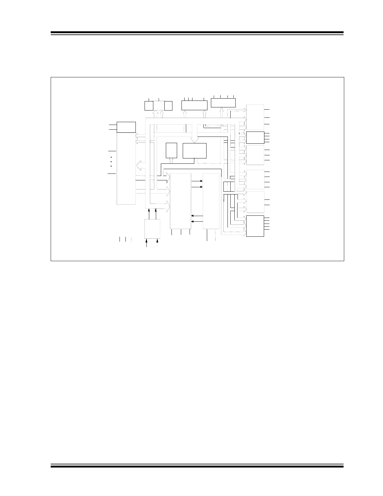
1.1
Block Diagram
1.2
3 Volt Operation / 5 Volt Tolerance
The LPC47B27x is a 3.3 Volt part. It is intended solely for 3.3V applications. Non-LPC bus pins are 5V tolerant; that is,
the input voltage is 5.5V max, and the I/O buffer output pads are backdrive protected.
The LPC interface pins are 3.3 V only. These signals meet PCI DC specifications for 3.3V signaling. These pins are:
LAD[3:0]
nLFRAME
nLDRQ
nLPCPD
The input voltage for all other pins is 5.5V max. These pins include all non-LPC Bus pins and the following pins:
nPCI_RESET
PCI_CLK
SER_IRQ
nIO_PME
FIGURE 1-1:
LPC47B27X BLOCK DIAGRAM
nDSR1, nDCD1, nRI1, nDTR1
TXD1, nCTS1, nRTS1
nINIT , nALF
LPC BUS
INTERFACE
MULTI-MODE
PARALLEL
PORT/FDC
MUX
16C550
COMPATIBLE
SERIAL
PORT 1
16C550
COMPATIBLE
SERIAL
PORT 2 WITH
INFRARED
ADDRESS BUS
DATA BUS
CLOCK
GEN
CLOCKI
14MHz
nINDEX
nTRK0
nDSKCHG
nWRPRT
nWGATE
DENSEL
nDIR
nSTEP
nHDSEL
nDS0
nMTR0
RDATA
RCLOCK
WDATA
WCLOCK
nWDATA nRDATA
TXD2(IRTX), nCTS2, nRTS2
*
RXD2(IRRX)
*
nDSR2, nDCD2, nRI2, nDTR2
*
RXD1
PD0-7
BUSY, SLCT, PE,
nERROR, nACK
nSTB, nSLCTIN,
SMSC
PROPRIETARY
82077
COMPATIBLE
VERTICAL
FLOPPYDISK
CONTROLLER
CORE
DIGITAL
DATA
SEPARATOR
WITH WRITE
PRECOM-
PENSATION
IRRX, IRTX
DRVDEN0
DRVDEN1
*
SERIAL
IRQ
SER_IRQ
PCI_CLK
8042
KCLK
KDATA
MCLK
MDATA
GATEA20, KRESET
PME
Vcc Vss
nIO_PME
WDT
*
Denotes Multifunction Pins
CLK32
32KHz
V
TR
SMI
LPC Bus
Signals
CONFIGURATION
REGISTERS
CONTROL BUS
Fan
Control
FAN1*
FAN2*
FAN_TACH1*
FAN_TACH2*
GENERAL
PURPOSE
I/O
GP1[0:7]*
GP2[0:2,4:7]*
MPU-401
SERIAL
PORT
MIDI_IN
MIDI_OUT
Game Port
...
Game Port Signals*
(1-Dual)
GP3[0:7]*, GP4[0:3]*
GP5[0:7]*, GP6[0:1]*
ACPI
BLOCK
nIO_SMI

LPC47B27x
DS00002492A-page 6
2004-2017 Microchip Technology Inc.
1.3
Reference Documents
1.
Microchip Consumer Infrared Communications Controller (CIrCC) V1.X
2.
IEEE 1284 Extended Capabilities Port Protocol and ISA Standard, Rev. 1.14, July 14, 1993
3.
Hardware Description of the 8042, Intel 8 bit Embedded Controller Handbook
4.
PCI Bus Power Management Interface Specification, Rev. 1.0, Draft, March 18, 1997
5.
Low Pin Count (LPC) Interface Specification, Revision 1.0, September 29, 1997, Intel document
6.
Application Note, AN 8.8: Using the Enhanced Keyboard and Mouse Wakeup Feature in SMSC Super I/O Parts
7.
Application Note, AN 9.3: Application Considerations When Using the Powerdown Feature of SMSC Floppy Disk
Controllers
2004-2017 Microchip Technology Inc.
DS00002492A-page 7
LPC47B27x
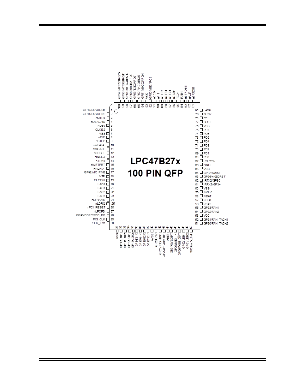
2.0
PIN CONFIGURATION
FIGURE 2-1:
LPC47B27X 100 PIN QFP
LPC47B27x
DS00002492A-page 8
2004-2017 Microchip Technology Inc.
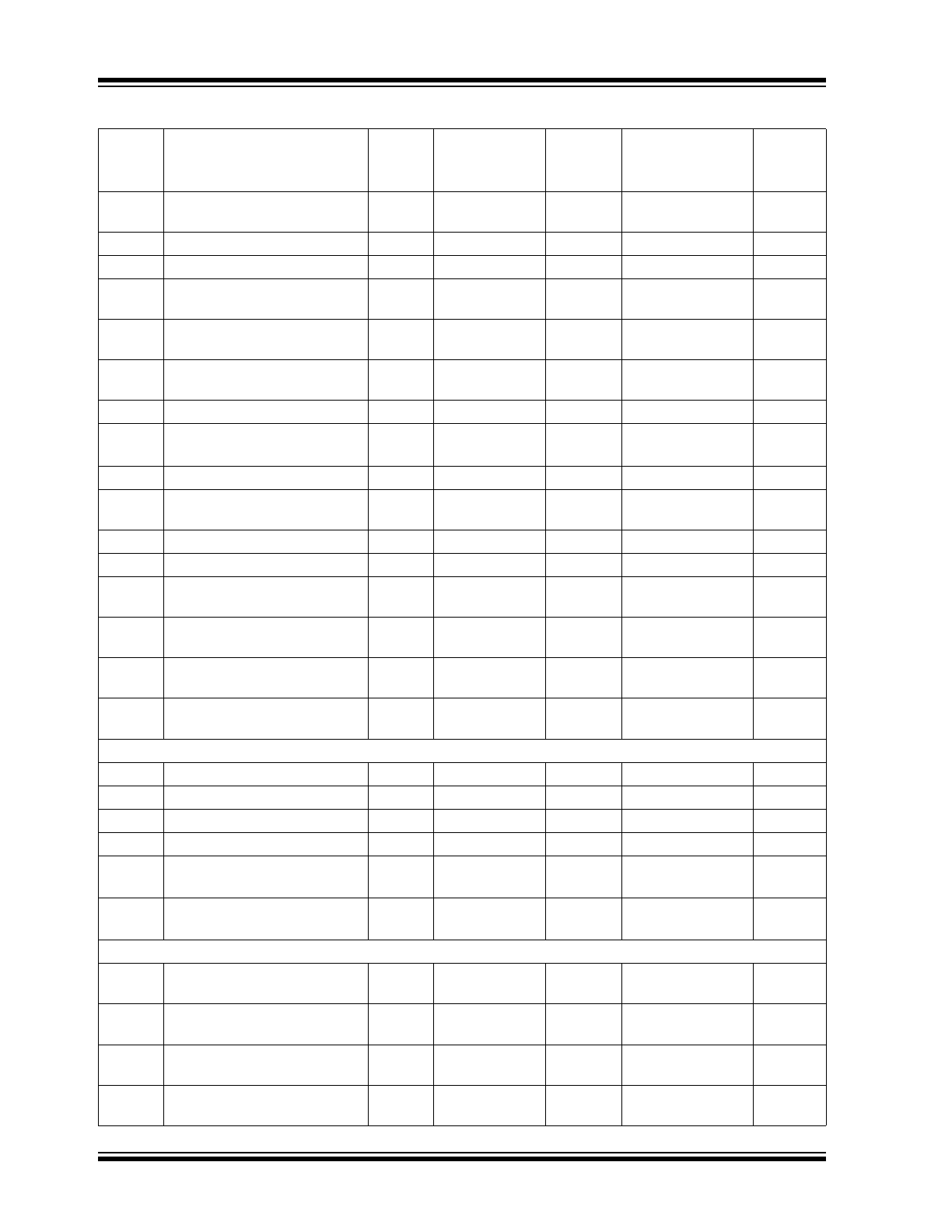
TABLE 2-1:
DESCRIPTION OF PIN FUNCTIONS
Pin No./
QFP
Name
Total
Symbol
Buffer
Type
Buffer Type per
Function
(
Note 1
)
Notes
PROCESSOR/HOST LPC INTERFACE (10)
23:20
Multiplexed Command,
Address, Data [3:0]
4
LAD[3:0]
PCI_IO
PCI_IO
24
Frame
1
nLFRAME
PCI_I
PCI_I
25
Encoded DMA Request
1
nLDRQ
PCI_O
PCI_O
26
PCI Reset
1
nPCI_RESET
PCI_I
PCI_I
27
Power Down
1
nLPCPD
PCI_I
PCI_I
Note 2
29
PCI Clock
1
PCI_CLK
PCI_ICL
K
PCI_ICLK
30
Serial IRQ
1
SER_IRQ
PCI_IO
PCI_IO
CLOCKS (2)
6
32.768kHz Trickle Clock Input
1
CLOCKI32
IS
IS
Note 3
19
14.318MHz Clock Input
1
CLOCKI
IS
IS
FAN CONTROL (4)
51
General Purpose I/O
/Fan Tachometer 2
1
GP30/
FAN_TACH2
IO8
(I/O8/OD8)/I
52
General Purpose I/O
/Fan Tachometer 1
1
GP31/
FAN_TACH1
IO8
(I/O8/OD8)/I
54
General Purpose I/O
/Fan Speed Control 2
1
GP32/FAN2
IO12
(I/O12/OD12)/
(O12/OD12)
Note 4
55
General Purpose I/O
/Fan Speed Control 1
1
GP33/FAN1
IO12
(I/O12/OD12)/
(O12/OD12)
Note 4
INFRARED INTERFACE (2)
61
Infrared Rx
/General Purpose I/O
1
IRRX2/GP34
IS/O8
IS/(IS/O8/OD8)
62
Infrared Tx
/General Purpose I/O
1
IRTX2/GP35
IO12
O12/(I/O12/
OD12)
Note 5
,
6
POWER PINS (10)
53,
65,93
+3.3 Volt Supply Voltage
3
VCC
7, 31,
60,76
Ground
4
VSS
40
Analog Ground
1
AVSS
44
Reference Voltage
1
VREF
18
+3.3 Volt Standby Supply
Voltage
1
VTR
Note 8
FDD INTERFACE (14)
16
Read Disk Data
1
nRDATA
IS
IS
11
Write Gate
1
nWGATE
O12
(O12/OD12)
10
Write Disk Data
1
nWDATA
O12
(O12/OD12)
12
Head Select
1
nHDSEL
O12
(O12/OD12)
2004-2017 Microchip Technology Inc.
DS00002492A-page 9
LPC47B27x
8
Step Direction
1
nDIR
O12
(O12/OD12)
9
Step Pulse
1
nSTEP
O12
(O12/OD12)
4
Disk Change
1
nDSKCHG
IS
IS
5
Drive Select 0
1
nDS0
O12
(O12/OD12)
3
Motor On 0
1
nMTR0
O12
(O12/OD12)
15
Write Protected
1
nWRTPRT
IS
IS
14
Track 0
1
nTRKO
IS
IS
13
Index Pulse Input
1
nINDEX
IS
IS
1
General Purpose I/O/Drive
Density Select 0
1
GP40/
DRVDEN0
IO12
(I/O12/OD12)/
(O12/OD12)
2
General Purpose I/O/Drive
Density Select 1
1
GP41/
DRVDEN1
IO12
(I/O12/OD12)/
(O12/OD12)
SERIAL PORT 1 INTERFACE (8)
84
Receive Serial Data 1
1
RXD1
IS
IS
85
Transmit Serial Data 1
1
TXD1
O12
O12
Note 12
87
Request to Send 1
1
nRTS1/
SYSOP
O8
O8
88
Clear to Send 1
1
nCTS1
I
I
89
Data Terminal Ready 1
1
nDTR1
O6
O6
86
Data Set Ready 1
1
nDSR1
I
I
91
Data Carrier Detect 1
1
nDCD1
I
I
90
Ring Indicator 1
1
nRI1
I
I
SERIAL PORT 2 INTERFACE (8)
95
General Purpose I/O
/Receive Serial Data 2 /IRQ5
1
GP52/RXD2/
IRQ5
IS/O8
(IS/O8/OD8)/ IS/
IS
96
General Purpose I/O
/Transmit Serial Data 2 /IRQ7
1
GP53/TXD2/
IRQ7
IO12
(I/O12/OD12)/
O12/I
Note 5
,
6
,
7
98
General Purpose I/O
/Request to Send 2/IRQ10
1
GP55/ nRTS2/
IRQ10
IO8
(I/O8/OD8)/ O8/I
99
General Purpose I/O
/Clear to Send 2/IRQ11
1
GP56/nCTS2/
IRQ11
IO8
(I/O8/OD8)/I/I
100
General Purpose I/O
/Data Terminal Ready/IRQ15
1
GP57/nDTR2/
IRQ15
IO8
(I/O8/OD8)/ O8/I
97
General Purpose I/O
/Data Set Ready 2/IRQ9
1
GP54/nDSR2/
IRQ9
IO8
(I/O8/OD8)/I/I
94
General Purpose I/O/Data
Carrier Detect 2/IRQ4
1
GP51/ nDCD2/
IRQ4
IO8
(I/O8/OD8)/I/I
92
General Purpose I/O/Ring
Indicator 2/IRQ3
1
GP50/nRI2/
IRQ3
IO8
(I/O8/OD8)/I/I
PARALLEL PORT INTERFACE (17)
66
Initiate Output/FDC Direction
Control
1
nINIT /nDIR
OP14
(OD14/OP14)/
OD14
TABLE 2-1:
DESCRIPTION OF PIN FUNCTIONS (CONTINUED)
Pin No./
QFP
Name
Total
Symbol
Buffer
Type
Buffer Type per
Function
(
Note 1
)
Notes
LPC47B27x
DS00002492A-page 10
2004-2017 Microchip Technology Inc.
67
Printer Select Input/FDC Step
Pulse
1
nSLCTIN /
nSTEP
OP14
(OD14/OP14)/
OD14
68
Port Data 0/FDC Index
1
PD0 /nINDEX
IS/OP14
IOP14/IS
69
Port Data 1/FDC Track 0
1
PD1 /nTRK0
IS/OP14
IOP14/IS
70
Port Data 2/FDC Write
Protected
1
PD2 /
nWRTPRT
IS/OP14
IOP14/IS
71
Port Data 3/FDC Read Disk
Data
1
PD3 /nRDATA
IS/OP14
IOP14/IS
72
Port Data 4/FDC Disk Change
1
PD4 /
nDSKCHG
IS/OP14
IOP14/IS
73
Port Data 5
1
PD5
IOP14
IOP14
74
Port Data 6/
FDC Motor On 0
1
PD6/nMTR0
IOP14
IOP14/OD14
75
Port Data 7
1
PD7
IOP14
IOP14
77
Printer Selected Status/FDC
Write Gate
1
SLCT /
nWGATE
IO12
I/OD12
78
Paper End/FDC Write Data
1
PE /nWDATA
IO12
I/OD12
79
Busy/FDC Motor On
1
BUSY /nMTR1
IO12
I/OD12
80
Acknowledge/FDC Drive
Select 1
1
nACK /nDS1
I/OD12
I/OD12
81
Error/FDC Head Select
1
nERROR /
nHDSEL
IO12
I/OD12
82
Autofeed Output/FDC Density
Select
1
nALF /
nDRVDEN0
OP14
(OD14/OP14)/
OD14
83
Strobe Output/FDC Drive
Select
1
nSTROBE /
nDS0
OP14
(OD14/OP14)/
OD14
KEYBOARD/MOUSE INTERFACE (6)
56
Keyboard Data
1
KDAT
IOD16
IOD16
57
Keyboard Clock
1
KCLK
IOD16
IOD16
58
Mouse Data
1
MDAT
IOD16
IOD16
59
Mouse Clock
1
MCLK
IOD16
IOD16
63
General Purpose I/O
/Keyboard Reset
1
GP36/
nKBDRST
IO8
(I/O8/OD8)/ O8
Note 10
64
General Purpose I/O
/Gate A20
1
GP37/A20M
IO8
(I/O8/OD8)/ O8
Note 10
GENERAL PURPOSE I/O (19)
32
General Purpose I/O /Joystick
1 Button 1
1
GP10/J1B1
IS/O8
(IS/O8/OD8)/ IS
33
General Purpose I/O /Joystick
1 Button 2
1
GP11/J1B2
IS/O8
(IS/O8/OD8)/ IS
34
General Purpose I/O /Joystick
2 Button 1
1
GP12/J2B1
IS/O8
(IS/O8/OD8)/ IS
35
General Purpose I/O /Joystick
2 Button 2
1
GP13/J2B2
IS/O8
(IS/O8/OD8)/ IS
TABLE 2-1:
DESCRIPTION OF PIN FUNCTIONS (CONTINUED)
Pin No./
QFP
Name
Total
Symbol
Buffer
Type
Buffer Type per
Function
(
Note 1
)
Notes