
2018 Microchip Technology Inc.
DS20005525A-page 1
SY54011R
Features
• 1.2V/1.8V CML 1:2 Fanout Buffer
• Guaranteed AC Performance over Temperature
and Voltage:
- DC-to->3.2 Gbps Throughput
- <300 ps Propagation Delay (IN-to-Q)
- <15 ps Within-Device Skew
- <95 ps Rise/Fall Times
• Ultra-Low Jitter Design
- 50 fs
RMS
Typical Additive Phase Jitter
• High Speed CML Outputs
• 2.5V ±5%, 1.2V/1.8V ±5% Power Supply
Operation
• Industrial Temperature Range: –40°C to +85°C
• Available in 16-pin (3 mm x 3 mm) QFN Package
Applications
• Data Distribution: OC-48, OC-48+FEC
• SONET Clock and Data Distribution
• Fibre Channel Clock and Data Distribution
• Gigabit Ethernet Clock and Data Distribution
Markets
• Storage
• ATE
• Test and Measurement
• Enterprise Networking Equipment
• High-End Servers
• Access
• Metro Area Network Equipment
General Description
The SY54011R is a fully differential, low-voltage
1.2V/1.8V CML 1:2 fanout buffer. It is optimized to
provide two identical output copies with less than 15 ps
of skew and 50 fs
RMS
of typical additive phase jitter.
The SY54011R can process clock signals as fast as
3.2 GHz or data patterns up to 3.2 Gbps.
The differential input includes a unique, 3-pin input
termination architecture that interfaces to LVPECL,
LVDS or CML differential signals, (AC- or DC-coupled
from a 2.5V driver) as small as 100 mV (200 mV
PP
)
without any level-shifting or termination resistor
networks in the signal path. For AC-coupled input
interface applications, an integrated voltage reference
(V
REF-AC
) is provided to bias the V
T
pin. The outputs
are CML, with extremely fast rise/fall times less than
95 ps.
The SY54011R operates from a 2.5V ±5% core supply
and a 1.2V or 1.8V ±5% output supply and is
guaranteed over the full industrial temperature range (–
40°C to +85°C). The SY54011R is part of the high
speed, Precision Edge
®
product line.
Package Type
SY54011R
3x3 QFN
(Top View)
IN
VT
VREF-AC
/IN
Q0
/Q0
/Q1
Q1
VCCO
GND
GND
VCC
VCCO
GND
GND
VCC
1
2
3
4
5 6
7 8
12
11
10
9
16 15 14 13
Low-Voltage 1.2V/1.8V CML 1:2 Fanout Buffer, 3.2 Gbps, 3.2 GHz
United States Patent No. RE44,134
SY54011R
DS20005525A-page 2
2018 Microchip Technology Inc.
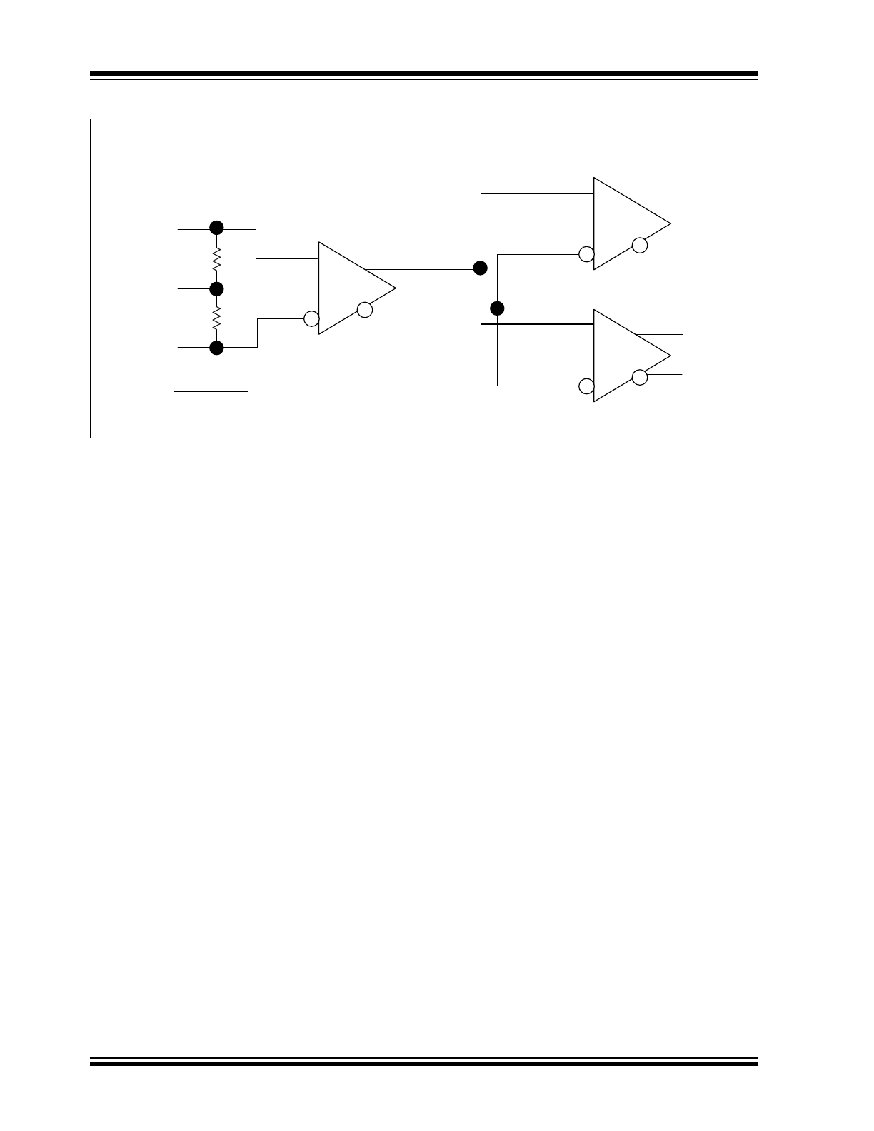
Functional Block Diagram
SY54011R
3
3 QFN
IN
V
T
/IN
V
REF-AC
50
50
Q0
/Q0
Q1
/Q1
2018 Microchip Technology Inc.
DS20005525A-page 3
SY54011R
1.0
ELECTRICAL CHARACTERISTICS
Absolute Maximum Ratings †
Supply Voltage (V
CC
) ................................................................................................................................ –0.5V to +3.0V
Supply Voltage (V
CCO
).............................................................................................................................. –0.5V to +2.7V
V
CC
- V
CCO
...............................................................................................................................................................<1.8V
V
CCO
- V
CC
...............................................................................................................................................................<0.5V
Input Voltage (V
IN
) ....................................................................................................................................... –0.5V to V
CC
CML Output Voltage (V
OUT
) ................................................................................................................0.6V to V
CCO
+0.5V
Current (V
T
)
Source or sink current on V
T
pin...........................................................................................................±100 mA
Input Current
Source or sink current on (IN, /IN) ..........................................................................................................±50 mA
Current (V
REF-AC
)
Source or sink current on V
REF-AC
(
Note 1
)...........................................................................................±0.5 mA
Operating Ratings ††
Supply Voltage (V
CC
) ............................................................................................................................ 2.375V to 2.625V
(V
CCO
)................................................................................................................................ 1.14V to 1.9V
†
Notice: Permanent device damage may occur if absolute maximum ratings are exceeded. This is a stress rating only
and functional operation is not implied at conditions other than those detailed in the operational sections of this data
sheet. Exposure to absolute maximum ratings conditions for extended periods may affect device reliability.
††
Notice: The data sheet limits are not guaranteed if the device is operated beyond the operating ratings.
Note 1:
Due to the limited drive capability, use for input of the same package only.
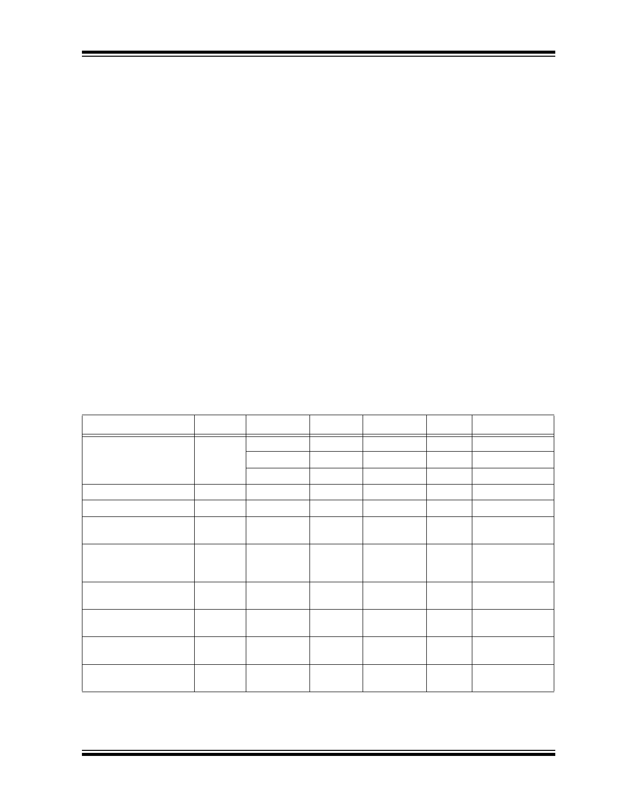
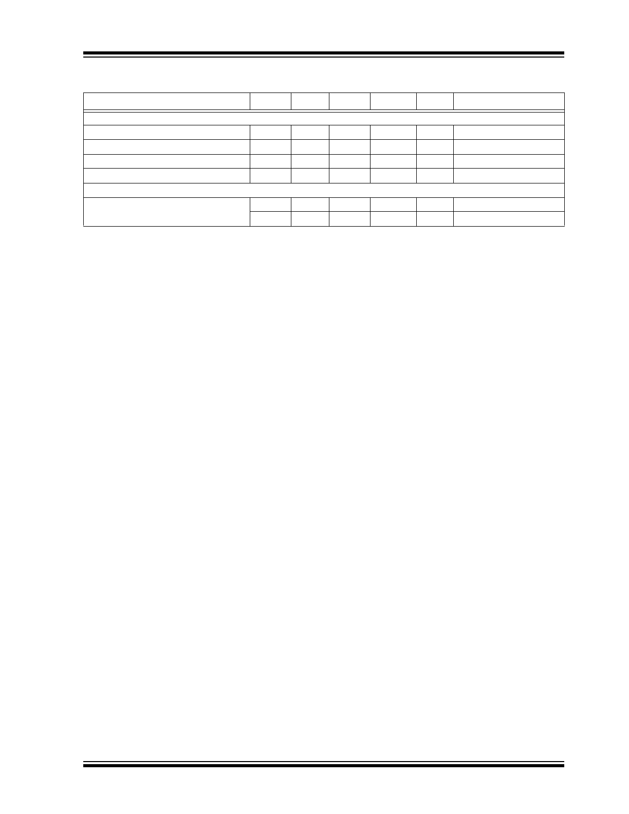
TABLE 1-1:
ELECTRICAL CHARACTERISTICS (
Note 1
)
Electrical Characteristics:
Unless otherwise indicated, T
A
= –40°C to +85°C.
Parameters
Sym.
Min.
Typ.
Max.
Units
Conditions
Power Supply Voltage
Range
V
CC
2.375
2.500
2.625
V
V
CC
1.140
1.200
1.260
V
V
CCO
1.700
1.800
1.900
V
V
CCO
Power Supply Current
I
CC
—
15
22
mA
Max. V
CC
Power Supply Current
I
CCO
—
32
42
mA
No Load. V
CCO
Input Resistance
(IN-to-V
T
, /IN-to-V
T
)
R
IN
45
50
55
Ω
—
Differential Input
Resistance
(IN-to-/IN)
R
DIFF_IN
90
100
110
Ω
—
Input HIGH Voltage (IN,
/IN)
V
IH
1.2
—
V
CC
V
IN, /IN
Input LOW Voltage (IN,
/IN)
V
IL
0.2
—
V
IH
– 0.1
V
V
IL
with V
IH
of
1.2V
Input HIGH Voltage (IN,
/IN)
V
IH
1.140
—
V
CC
V
IN, /IN
Input LOW Voltage (IN,
/IN)
V
IL
0.66
—
V
IH
– 0.10
V
V
IL
with V
IH
of
1.140V, (1.2V-5%)
Note 1:
The circuit is designed to meet the DC specifications shown in the above table after thermal equilibrium
has been established.
2:
Due to the limited drive capability, use for input of the same package only.
SY54011R
DS20005525A-page 4
2018 Microchip Technology Inc.
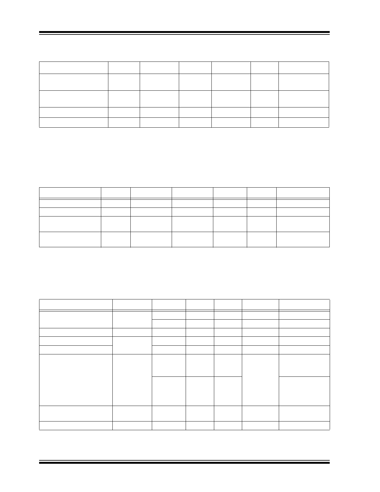
TABLE 1-3:
AC ELECTRICAL CHARACTERISTICS
Input Voltage Swing (IN,
/IN)
V
IN
0.1
—
1.0
V
See
Figure 6-3
Differential Input Voltage
Swing (|IN, /IN|)
V
DIFF_IN
0.2
—
2.0
V
See
Figure 6-5
Output Reference Voltage
V
REF-AC
V
CC
– 1.3
V
CC
– 1.15
V
CC
– 1.0
V
Note 2
Voltage from Input to V
T
V
T_IN
—
—
1.28
V
—
TABLE 1-1:
ELECTRICAL CHARACTERISTICS (
Note 1
) (CONTINUED)
Electrical Characteristics:
Unless otherwise indicated, T
A
= –40°C to +85°C.
Parameters
Sym.
Min.
Typ.
Max.
Units
Conditions
Note 1:
The circuit is designed to meet the DC specifications shown in the above table after thermal equilibrium
has been established.
2:
Due to the limited drive capability, use for input of the same package only.
TABLE 1-2:
CML OUTPUTS DC ELECTRICAL CHARACTERISTICS (
Note 1
)
V
CCO
= 1.14V to 1.26V, R
L
= 50Ω to V
CCO
,
V
CCO
= 1.7V to 1.9V, R
L
= 50Ω to V
CCO
or 100Ω across the outputs,
V
CC
= 2.375V to 2.625V. T
A
= –40°C to +85°C, unless otherwise stated.
Parameters
Sym.
Min.
Typ.
Max.
Units
Conditions
Output HIGH Voltage
V
OH
V
CCO
– 0.020
V
CCO
– 0.010
V
CCO
V
R
L
= 50Ω to V
CCO
Output Voltage Swing
V
OUT
300
390
475
mV
See
Figure 6-3
Differential Output
Voltage Swing
V
DIFF_OUT
600
780
950
mV
See
Figure 6-5
Output Source
Impedance
R
OUT
45
50
55
Ω
—
Note 1:
The circuit is designed to meet the DC specifications shown in the above table after thermal equilibrium
has been established.
V
CCO
= 1.14V to 1.26V, R
L
= 50Ω to V
CCO
,
V
CCO
= 1.7V to 1.9V, R
L
= 50Ω to V
CCO
or 100Ω across the outputs,
V
CC
= 2.375V to 2.625V. T
A
= –40°C to +85°C, unless otherwise stated.
Parameters
Sym.
Min.
Typ.
Max.
Units
Conditions
Maximum Frequency
f
MAX
3.2
—
—
Gbps
NRZ Data
3.2
—
—
GHz
V
OUT
> 200 mV
Propagation Delay IN-to-Q
t
PD
150
205
300
ps
Figure 6-1
Within Device Skew
t
SKEW
—
3
15
ps
Note 1
Part-to-Part Skew
—
—
75
ps
Note 2
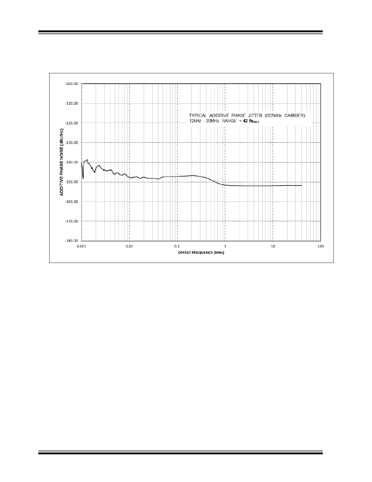
Additive Phase Jitter
t
JITTER
—
42
—
fs
RMS
Carrier = 622 MHz
Integration Range:
12 kHz – 20 MHz
—
250
—
Carrier =
156.25 MHz.
Integration Range:
12 kHz – 20 MHz
Output Rise/Fall Times
(20% to 80%)
t
R
, t
F
30
60
95
ps
At full output
swing.
Duty Cycle
—
47
—
53
%
Differential I/O
Note 1:
Within device skew is measured between two different outputs under identical input transitions.
2:
Part-to-part skew is defined for two parts with identical power supply voltages at the same temperature
and no skew at the edges at the respective inputs.
2018 Microchip Technology Inc.
DS20005525A-page 5
SY54011R
TEMPERATURE SPECIFICATIONS (
Note 1
)
Parameters
Sym.
Min.
Typ.
Max.
Units
Conditions
Temperature Ranges
Operating Ambient Temperature Range
T
A
–40
—
+85
°C
—
Junction Operating Temperature
T
J
—
—
+125
°C
—
Storage Temperature Range
T
S
–65
—
+150
°C
—
Lead Temperature
—
—
+260
—
°C
Soldering, 20 sec.
Package Thermal Resistance (
Note 2
)
Thermal Resistance, 3 x 3 QFN-16LD
JA
—
75
—
°C/W
Still-Air
JB
—
33
—
°C/W
Junction-to-board
Note 1:
The maximum allowable power dissipation is a function of ambient temperature, the maximum allowable
junction temperature and the thermal resistance from junction to air (i.e., T
A
, T
J
,
JA
). Exceeding the max-
imum allowable power dissipation will cause the device operating junction temperature to exceed the max-
imum +125°C rating. Sustained junction temperatures above +125°C can impact the device reliability.
2:
Package thermal resistance assumes exposed pad is soldered (or equivalent) to the device's most nega-
tive potential on the PCB. θ
JA
and Ψ
Jb
values are determined for a 4-layer board in still-air number, unless
otherwise stated.
SY54011R
DS20005525A-page 6
2018 Microchip Technology Inc.
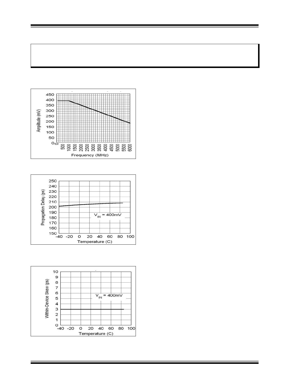
2.0
TYPICAL OPERATING CHARACTERISTICS
For
Figure 2-1
through
Figure 2-3
, V
CC
= 2.5V, V
CCO
= 1.2V, GND = 0V, V
IN
= 100 mV; R
L
= 50Ω to 1.2V; T
A
= +25°C,
unless otherwise stated.
FIGURE 2-1:
Amplitude vs. Frequency.
FIGURE 2-2:
Propagation Delay vs.
Temperature.
FIGURE 2-3:
Within-Device Skew vs.
Temperature.
Note:
The graphs and tables provided following this note are a statistical summary based on a limited number of
samples and are provided for informational purposes only. The performance characteristics listed herein
are not tested or guaranteed. In some graphs or tables, the data presented may be outside the specified
operating range (e.g., outside specified power supply range) and therefore outside the warranted range.
2018 Microchip Technology Inc.
DS20005525A-page 7
SY54011R
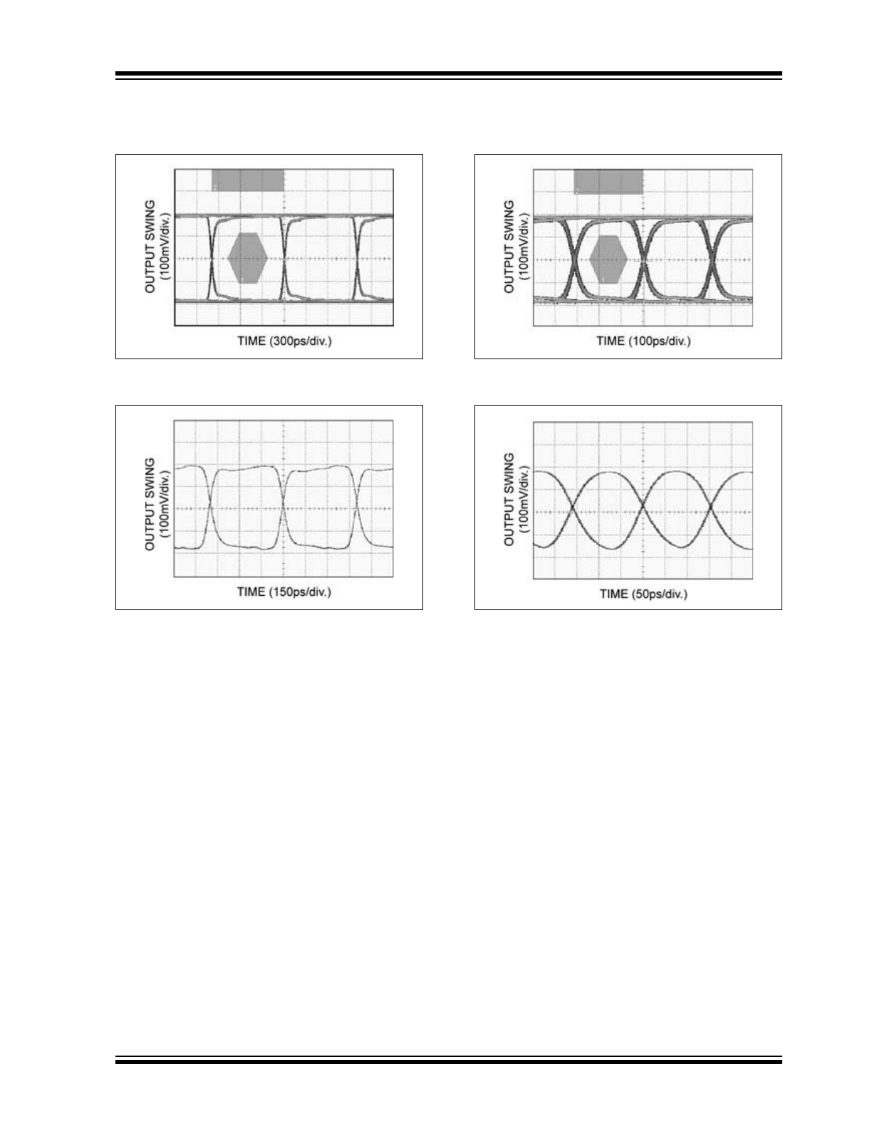
For
Figure 2-4
through
Figure 2-7
, V
CC
= 2.5V, V
CCO
= 1.2V, GND = 0V, V
IN
= 100 mV; R
L
= 50Ω to 1.2V,
Data Pattern: 2
23
-1; T
A
= +25°C, unless otherwise stated.
FIGURE 2-4:
1.0 Gbps Data.
FIGURE 2-5:
1.0 GHz Clock.
FIGURE 2-6:
3.2 Gbps Data.
FIGURE 2-7:
3.2 GHz Clock.
SY54011R
DS20005525A-page 8
2018 Microchip Technology Inc.
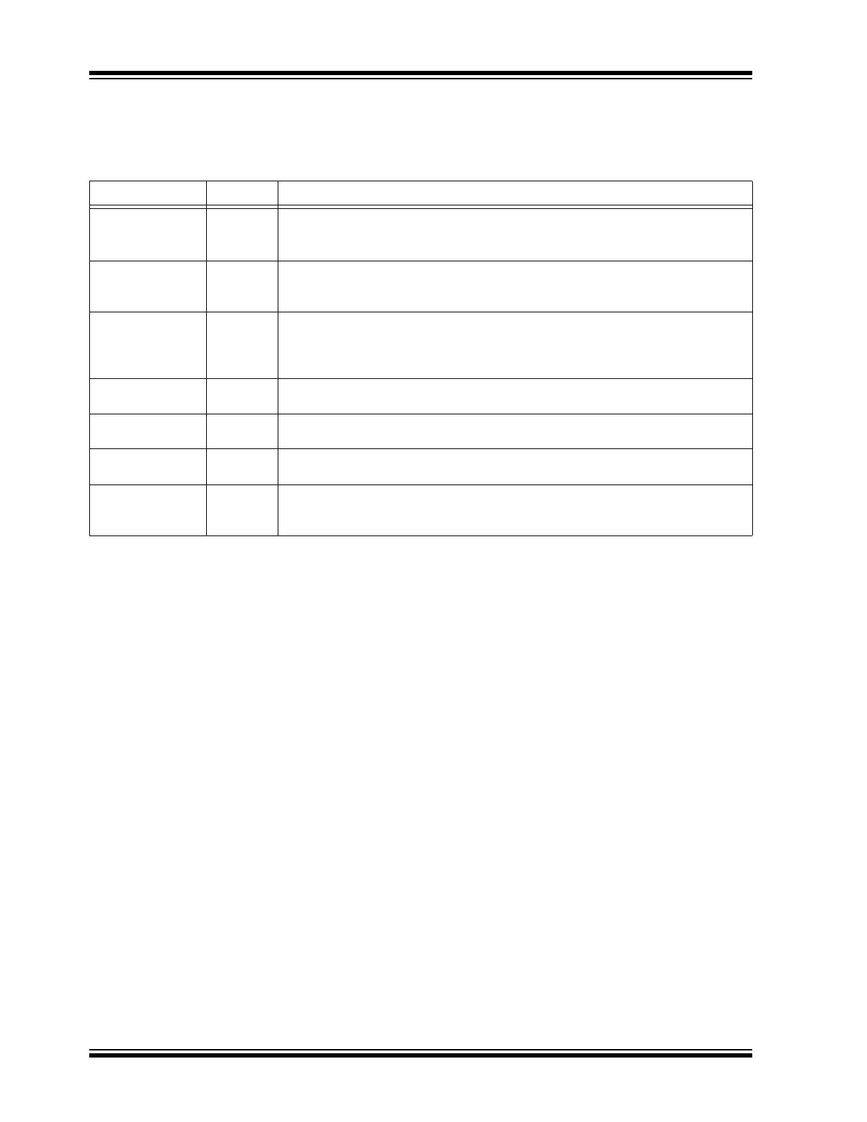
3.0
PIN DESCRIPTIONS
The descriptions of the pins are listed in
Table 3-1
.
TABLE 3-1:
PIN FUNCTION TABLE
Pin Number
Symbol
Description
1, 4
IN, /IN
Differential Input: This input pair is the differential signal input to the device. Input
accepts differential signals as small as 100 mV (200 mV
PP
). Each input pin
internally terminates with 50Ω to the V
T
pin.
2
V
T
Input Termination Center-Tap: Each side of the differential input pair terminates to
V
T
pin. This pin provides a center-tap to a termination network for maximum
interface flexibility. See the
Input Interface Applications
section.
3
V
REF-AC
Reference Voltage: This output biases to V
CC
– 1.150V. It is used for AC-coupling
inputs IN and /IN. Connect V
REF-AC
directly to the V
T
pin. Bypass with 0.1 µF low
ESR capacitor to V
CC
. Maximum sink/source current is ±0.5 mA. See the
Input
Interface Applications
section.
5, 16
V
CC
Positive Power Supply: Bypass with 0.1 µF/0.01 µF low ESR capacitors as close to
the V
CC
pins as possible. Supplies input and core circuitry.
8, 13
V
CCO
Output Supply: Bypass with 0.1 µF//0.01 µF low ESR capacitors as close to the
V
CCO
pins as possible. Supplies the output buffers.
6, 7, 14, 15
GND, EP Ground: Exposed pad must be connected to a ground plane that is the same
potential as the ground pins.
10, 9
11, 12
/Q1, Q1
/Q0, Q0
CML Differential Output Pairs: Differential buffered copies of the input signal. The
output swing is typically 390 mV. See the
Input Interface Applications
section for
termination information.

2018 Microchip Technology Inc.
DS20005525A-page 9
SY54011R
4.0
INTERFACE APPLICATIONS
For Input Interface Applications see
Figure 7-1
through
Figure 7-7
and for CML Output Termination see
Figure 8-1
through
Figure 8-4
.
4.1
CML Output Termination with
V
CCO
1.2V
For V
CCO
of 1.2V (see
Figure 8-1
), terminate the output
with 50Ω-to-1.2V, DC-coupled, not 100Ω differentially
across the outputs.
If AC-coupling is used (see
Figure 8-4
), terminate into
50Ω-to-1.2V before the coupling capacitor and then
connect to a high value resistor to a reference voltage.
Do not AC couple with internally terminated receiver.
For example, 50Ω ANY-IN input. AC-coupling will offset
the output voltage by 200 mV and this offset voltage will
be too low for proper driver operation.
Any unused output pair needs to be terminated when
V
CCO
is 1.2V, do not leave floating.
4.2
CML Output Termination with
V
CCO
1.8V
For V
CCO
of 1.8V,
Figure 8-1
and
Figure 8-2
, terminate
with either 50Ω-to-V
CCO
or 100Ω differentially across
the outputs. AC- or DC-coupling is fine.
4.3
Input AC Coupling
The SY54011R input can accept AC coupling from any
driver. Tie V
T
to V
REF-AC
and bypass with a 0.1 µF
capacitor as shown in
Figure 7-3
and
Figure 7-4
.
SY54011R
DS20005525A-page 10
2018 Microchip Technology Inc.
5.0
ADDITIVE PHASE NOISE PLOTS
V
CC
= +2.5V, GND = 0V, T
A
= +25°C.
FIGURE 5-1:
Typical Additive Phase Jitter: 622 MHz Carrier, 12 kHz to 20 MHz Range, 42 fs
RMS
.