

2005-2016 Microchip Technology Inc.
DS20001942G-page 1
MCP9700/9700A
MCP9701/9701A
Features
• Tiny Analog Temperature Sensor
• Available Packages:
- SC70-5, SOT-23-3, TO-92-3
• Wide Temperature Measurement Range:
- -40°C to +125°C (Extended Temperature)
- -40°C to +150°C (High Temperature)
(MCP9700, SOT-23-3 and SC70-5 only)
• Accuracy:
- ±2°C (max.), 0°C to +70°C
(MCP9700A/9701A)
- ±4°C (max.), 0°C to +70°C
(MCP9700/9701)
• Optimized for Analog-to-Digital Converters (ADCs):
- 10.0 mV/°C (typical)
(MCP9700/9700A)
- 19.5 mV/°C (typical)
(MCP9701/9701A)
• Wide Operating Voltage Range:
- V
DD
= 2.3V to 5.5V
(MCP9700/9700A)
- V
DD
= 3.1V to 5.5V
(MCP9701/9701A)
• Low Operating Current: 6 µA (typical)
• Optimized to Drive Large Capacitive Loads
Typical Applications
• Hard Disk Drives and Other PC Peripherals
• Entertainment Systems
• Home Appliance
• Office Equipment
• Battery Packs and Portable Equipment
• General Purpose Temperature Monitoring
General Description
MCP9700/9700A and MCP9701/9701A sensors with
Linear Active Thermistor Integrated Circuit (IC) com-
prise a family of analog temperature sensors that
convert temperature to analog voltage.
The low-cost, low-power sensors feature an accuracy
of ±2°C from 0°C to +70°C (MCP9700A/9701A) and
±4°C from 0°C to +70°C (MCP9700/9701) while
consuming 6 µA (typical) of operating current.
Unlike resistive sensors, e.g., thermistors, the Linear
Active Thermistor IC does not require an additional
signal-conditioning circuit. Therefore, the biasing circuit
development overhead for thermistor solutions can be
avoided by implementing a sensor from these low-cost
devices. The Voltage Output pin (V
OUT
) can be directly
connected to the ADC input of a microcontroller. The
MCP9700/9700A and MCP9701/9701A temperature
coefficients are scaled to provide a 1°C/bit resolution
for an 8-bit ADC with a reference voltage of 2.5V and
5V, respectively. The MCP9700/9700A output 0.1°C/bit
for a 12-bit ADC with 4.096V reference.
The MCP9700/9700A and MCP9701/9701A provide a
low-cost solution for applications that require measure-
ment of a relative change of temperature. When mea-
suring relative change in temperature from +25°C, an
accuracy of ±1°C (typical) can be realized from 0°C to
+70°C. This accuracy can also be achieved by applying
system calibration at +25°C.
In addition, this family of devices is immune to the
effects of parasitic capacitance and can drive large
capacitive loads. This provides printed circuit board
(PCB) layout design flexibility by enabling the device to
be remotely located from the microcontroller. Adding
some capacitance at the output also helps the output
transient response by reducing overshoots or
undershoots. However, capacitive load is not required
for the stability of sensor output.
Package Types
3-Pin SOT-23
MCP9700/9700A
MCP9701/9701A
3-Pin TO-92
1 2 3
GND
V
OUT
V
DD
Bottom
View
MCP9700/9700A
MCP9701/9701A
1
GND
V
DD
V
OUT
NC
4
1
2
3
5
5-Pin SC70
NC
MCP9700/9700A
MCP9701/9701A
GND
V
DD
V
OUT
3
1
2
Low-Power Linear Active Thermistor ICs
MCP9700/9700A and MCP9701/9701A
DS20001942G-page 2
2005-2016 Microchip Technology Inc.
1.0
ELECTRICAL
CHARACTERISTICS
Absolute Maximum Ratings †
V
DD
....................................................................... 6.0V
Storage Temperature......................... -65°C to +150°C
Ambient Temp. with Power Applied... -40°C to +150°C
Output Current .................................................±30 mA
Junction Temperature (T
J
).................................. 150°C
ESD Protection on All Pins (HBM:MM) ..... (4 kV:200V)
Latch-Up Current at Each Pin ....................... ±200 mA
† Notice: Stresses above those listed under “Maximum
Ratings” may cause permanent damage to the device. This is
a stress rating only and functional operation of the device at
those or any other conditions above those indicated in the
operational listings of this specification is not implied.
Exposure to maximum rating conditions for extended periods
may affect device reliability.
DC ELECTRICAL CHARACTERISTICS
Electrical Specifications: Unless otherwise indicated:
MCP9700/9700A: V
DD
= 2.3V to 5.5V, GND = Ground, T
A
= -40°C to +125°C and No load
MCP9701/9701A: V
DD
= 3.1V to 5.5V, GND = Ground, T
A
= -10°C to +125°C and No load
Parameter
Sym.
Min.
Typ.
Max.
Unit
Conditions
Power Supply
Operating Voltage Range
V
DD
V
DD
2.3
3.1
—
—
5.5
5.5
V
V
MCP9700/9700A
MCP9701/9701A
Operating Current
I
DD
—
6
12
µA
I
DD
—
—
15
µA
T
A
= 150°C
(
Note 1
)
Line Regulation
°C/V
DD
—
0.1
—
°C/V
Sensor Accuracy (
Notes 2
,
3
)
T
A
= +25°C
T
ACY
—
±1
—
°C
T
A
= 0°C to +70°C
T
ACY
-2.0
±1
+2.0
°C
MCP9700A/9701A
T
A
= -40°C to +125°C
T
ACY
-2.0
±1
+4.0
°C
MCP9700A
T
A
= -10°C to +125°C
T
ACY
-2.0
±1
+4.0
°C
MCP9701A
T
A
= 0°C to +70°C
T
ACY
-4.0
±2
+4.0
°C
MCP9700/9701
T
A
= -40°C to +125°C
T
ACY
-4.0
±2
+6.0
°C
MCP9700
T
A
= -10°C to +125°C
T
ACY
-4.0
±2
+6.0
°C
MCP9701
T
A
= -40°C to +150°C
T
ACY
-4.0
±2
+6.0
°C
HighTemperature (
Note 1
)
Sensor Output
Output Voltage, T
A
= 0°C
V
0°C
—
500
—
mV
MCP9700/9700A
Output Voltage, T
A
= 0°C
V
0°C
—
400
—
mV
MCP9701/9701A
Temperature Coefficient
T
C
—
10.0
—
mV/°C
MCP9700/9700A
T
C
—
19.5
—
mV/°C
MCP9701/9701A
Output Nonlinearity
V
ONL
—
±0.5
—
°C
T
A
= 0°C to +70°C
(
Note 3
)
Note 1:
MCP9700 with SC70-5 and SOT-23-3 packages only. The MCP9700 High Temperature is not available
with TO-92 package.
2:
The MCP9700/9700A family accuracy is tested with V
DD
= 3.3V, while the MCP9701/9701A accuracy is
tested with V
DD
= 5.0V.
3:
The MCP9700/9700A and MCP9701/9701A family is characterized using the first-order or linear equation,
as shown in
Equation 4-2
. Also refer to
Figure 2-16
.
4:
The MCP9700/9700A and MCP9701/9701A family is characterized and production tested with a
capacitive load of 1000 pF.
5:
SC70-5 package thermal response with 1x1 inch, dual-sided copper clad, TO-92-3 package thermal
response without PCB (leaded).
2005-2016 Microchip Technology Inc.
DS20001942G-page 3
MCP9700/9700A and MCP9701/9701A
Output Current
I
OUT
—
—
100
µA
Output Impedance
Z
OUT
—
20
—
I
OUT
= 100 µA, f = 500 Hz
Output Load Regulation
V
OUT
/
I
OUT
—
1
—
T
A
= 0°C to +70°C
I
OUT
= 100 µA
Turn-On Time
t
ON
—
800
—
µs
Typical Load Capacitance
C
LOAD
—
—
1000
pF
Note 4
SC-70 Thermal Response to 63%
t
RES
—
1.3
—
s
30°C (Air) to +125°C
(Fluid Bath)
(
Note 5
)
TO-92 Thermal Response to 63%
t
RES
—
1.65
—
s
DC ELECTRICAL CHARACTERISTICS (CONTINUED)
Electrical Specifications: Unless otherwise indicated:
MCP9700/9700A: V
DD
= 2.3V to 5.5V, GND = Ground, T
A
= -40°C to +125°C and No load
MCP9701/9701A: V
DD
= 3.1V to 5.5V, GND = Ground, T
A
= -10°C to +125°C and No load
Parameter
Sym.
Min.
Typ.
Max.
Unit
Conditions
Note 1:
MCP9700 with SC70-5 and SOT-23-3 packages only. The MCP9700 High Temperature is not available
with TO-92 package.
2:
The MCP9700/9700A family accuracy is tested with V
DD
= 3.3V, while the MCP9701/9701A accuracy is
tested with V
DD
= 5.0V.
3:
The MCP9700/9700A and MCP9701/9701A family is characterized using the first-order or linear equation,
as shown in
Equation 4-2
. Also refer to
Figure 2-16
.
4:
The MCP9700/9700A and MCP9701/9701A family is characterized and production tested with a
capacitive load of 1000 pF.
5:
SC70-5 package thermal response with 1x1 inch, dual-sided copper clad, TO-92-3 package thermal
response without PCB (leaded).
TEMPERATURE CHARACTERISTICS
Electrical Specifications: Unless otherwise indicated:
MCP9700/9700A: V
DD
= 2.3V to 5.5V, GND = Ground, T
A
= -40°C to +125°C and No load
MCP9701/9701A: V
DD
= 3.1V to 5.5V, GND = Ground, T
A
= -10°C to +125°C and No load
Parameters
Sym.
Min.
Typ.
Max.
Units
Conditions
Temperature Ranges
Specified Temperature Range
(
Note 1
)
T
A
-40
—
+125
°C
MCP9700/9700A
T
A
-10
—
+125
°C
MCP9701/9701A
T
A
-40
—
+150
°C
High Temperature
(MCP9700, SOT23-3
and SC70-5 only
)
Operating Temperature Range
T
A
-40
—
+125
°C
Extended Temperature
T
A
-40
—
+150
°C
High Temperature
Storage Temperature Range
T
A
-65
—
+150
°C
Thermal Package Resistances
Thermal Resistance, 5LD SC70
JA
—
331
—
°C/W
Thermal Resistance, 3LD SOT-23
JA
—
308
—
°C/W
Thermal Resistance, 3LD TO-92
JA
—
146
—
°C/W
Note 1:
Operation in this range must not cause T
J
to exceed Maximum Junction Temperature (+150°C).
MCP9700/9700A and MCP9701/9701A
DS20001942G-page 4
2005-2016 Microchip Technology Inc.
2.0
TYPICAL PERFORMANCE CURVES
Note: Unless otherwise indicated, MCP9700/9700A: V
DD
= 2.3V to 5.5V;
MCP9701/9701A: V
DD
= 3.1V to 5.5V;
GND = Ground, C
bypass
= 0.1 µF.
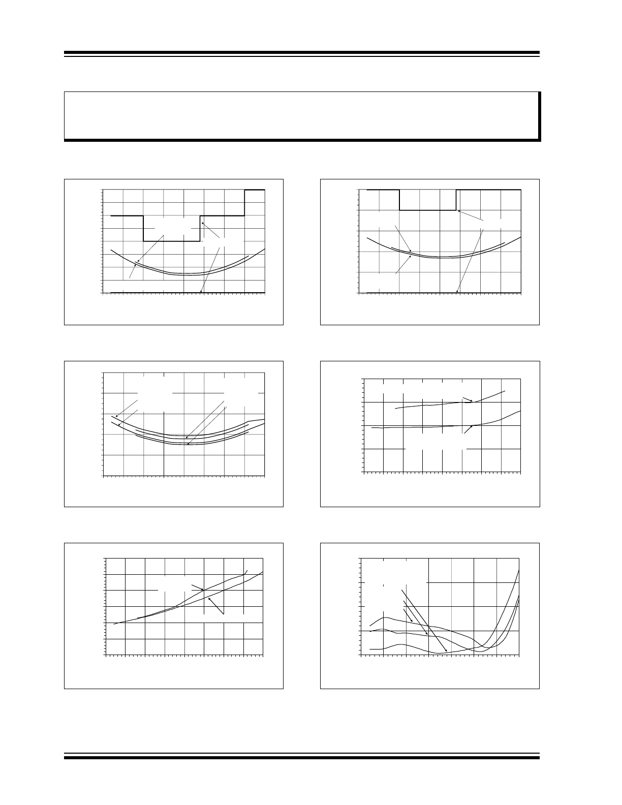
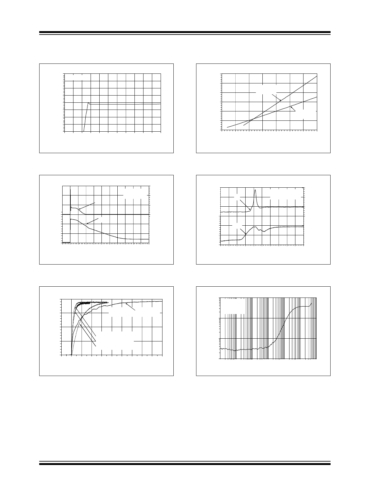
FIGURE 2-1:
Accuracy vs. Ambient
Temperature (MCP9700A/9701A).
FIGURE 2-2:
Accuracy vs. Ambient
Temperature, with V
DD
.
FIGURE 2-3:
Supply Current vs.
Temperature.
FIGURE 2-4:
Accuracy vs. Ambient
Temperature (MCP9700/9701).
FIGURE 2-5:
Changes in Accuracy vs.
Ambient Temperature (Due to Load).
FIGURE 2-6:
Load Regulation vs.
Ambient Temperature.
Note:
The graphs and tables provided following this note are a statistical summary based on a limited number of
samples and are provided for informational purposes only. The performance characteristics listed herein
are not tested or guaranteed. In some graphs or tables, the data presented may be outside the specified
operating range (e.g., outside specified power supply range) and therefore outside the warranted range.
-2.0
-1.0
0.0
1.0
2.0
3.0
4.0
5.0
6.0
-50 -25
0
25
50
75
100 125 150
Accuracy (°C)
T
A
(°C)
MCP9700A V
DD
= 3.3V
MCP9701A
V
DD
= 5.0V
Spec. Limits
-4.0
-2.0
0.0
2.0
4.0
6.0
-50
-25
0
25
50
75
100 125 150
Accuracy
(°C)
T
A
(°C)
MCP9701/
MCP9701A
V
DD
= 5.5V
V
DD
= 3.1V
MCP9700
MCP9700A
V
DD
= 5.5V
V
DD
= 2.3V
0.0
2.0
4.0
6.0
8.0
10.0
12.0
-50
-25
0
25
50
75
100
125
150
T
A
(°C)
I
DD
(µ
A
)
MCP9700/MCP9700A
MCP9701
MCP9701A
-4.0
-2.0
0.0
2.0
4.0
6.0
-50 -25
0
25
50
75
100 125 150
Accuracy (°C)
T
A
(°C)
MCP9700
V
DD
= 3.3V
MCP9701
V
DD
= 5.0V
Spec. Limits
-0.2
-0.1
0
0.1
0.2
-50
-25
0
25
50
75
100 125 150
T
A
(°C)
∆
A
cc
u
ra
c
y
D
u
e to Loa
d
(°
C)
MCP9701/MCP9701A
V
DD
= 5.0V
I
LOAD
= 100 µA
MCP9700/MCP9700A
V
DD
= 3.3V
0.0
1.0
2.0
3.0
4.0
-50
-25
0
25
50
75
100
125
T
A
(°C)
L
o
a
d
R
egu
la
ti
on
∆
V/
∆
I (
Ω
)
MCP9700/MCP9700A
MCP9701/MCP9701A
V
DD
= 3.3V
I
OUT
= 50 µA
I
OUT
= 100 µA
I
OUT
= 200 µA
2005-2016 Microchip Technology Inc.
DS20001942G-page 5
MCP9700/9700A and MCP9701/9701A
Note: Unless otherwise indicated, MCP9700/9700A: V
DD
= 2.3V to 5.5V;
MCP9701/9701A: V
DD
= 3.1V to 5.5V;
GND = Ground, C
bypass
= 0.1 µF.
FIGURE 2-7:
Output Voltage at 0°C
(MCP9700/9700A).
FIGURE 2-8:
Occurrences vs.
Temperature Coefficient (MCP9700/9700A).
FIGURE 2-9:
Line Regulation (
°C/
V
DD
)
vs. Ambient Temperature.
FIGURE 2-10:
Output Voltage at 0°C
(MCP9701/9701A).
FIGURE 2-11:
Occurrences vs.
Temperature Coefficient (MCP9701/9701A).
FIGURE 2-12:
Line Regulation (
°C/
V
DD
)
vs. Ambient Temperature.
0%
5%
10%
15%
20%
25%
30%
35%
40
0
42
0
44
0
46
0
48
0
50
0
52
0
54
0
56
0
58
0
60
0
V
0°C
(mV)
O
c
cu
rr
en
ces
V
DD
= 3.3V
108 samples
MCP9700A
MCP9700
0%
5%
10%
15%
20%
25%
30%
35%
40%
45%
9.
7
9.
8
9.
8
9.
9
10
.0
10
.1
10.
2
10.
2
10.
3
10.
4
10.
5
T
C
(mV/°C)
O
ccu
rr
ences
MCP9700
MCP9700A
V
DD
= 3.3V
108 samples
0.00
0.05
0.10
0.15
0.20
0.25
0.30
-50
-25
0
25
50
75
100
125
150
Normalized Line Regulation
(ǻ
°C/
ǻ
V
DD
)
T
A
(°C)
MCP9700/MCP9700A
V
DD
= 2.3V to 5.5V
MCP9700/MCP9700A
V
DD
= 2.3V to 4.0V
0%
5%
10%
15%
20%
25%
30%
35%
30
0
32
0
34
0
36
0
38
0
40
0
42
0
44
0
46
0
48
0
50
0
V
0°C
(mV)
O
c
cu
rr
en
ces
MCP9701
V
DD
= 5.0V
108 samples
MCP9701A
MCP9701
0%
5%
10%
15%
20%
25%
30%
35%
40%
45%
19
.2
19
.3
19
.3
19
.4
19
.5
19
.6
19
.7
19
.7
19
.8
19
.9
20
.0
T
C
(mV/°C)
O
ccu
rr
en
ces
MCP9701
MCP9701A
V
DD
= 5.0V
108 samples
0.00
0.05
0.10
0.15
0.20
0.25
0.30
-50
-25
0
25
50
75
100
125
Normalized Line Regulation
(ǻ
°C/
ǻ
V
DD
)
T
A
(°C)
MCP9701/MCP9701A
V
DD
= 3.1V to 5.5V
MCP9701/MCP9701A
V
DD
= 3.1V to 4.0V
MCP9700/9700A and MCP9701/9701A
DS20001942G-page 6
2005-2016 Microchip Technology Inc.
Note: Unless otherwise indicated, MCP9700/9700A: V
DD
= 2.3V to 5.5V;
MCP9701/9701A: V
DD
= 3.1V to 5.5V;
GND = Ground, C
bypass
= 0.1 µF.
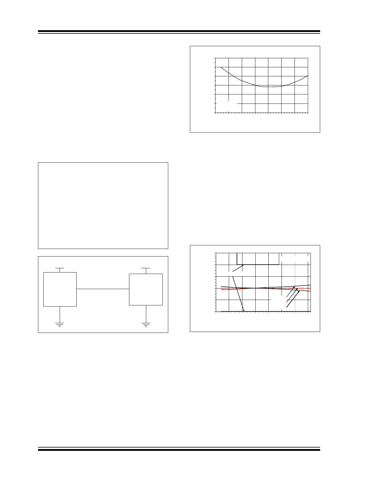
FIGURE 2-13:
Output Voltage vs. Power
Supply.
FIGURE 2-14:
Output vs. Settling Time to
Step V
DD
.
FIGURE 2-15:
Thermal Response
(Air-to-Fluid Bath).
FIGURE 2-16:
Output Voltage vs. Ambient
Temperature.
FIGURE 2-17:
Output vs. Settling Time to
Ramp V
DD
.
FIGURE 2-18:
Output Impedance vs.
Frequency.
0.0
0.2
0.4
0.6
0.8
1.0
1.2
1.4
1.6
0.0 0.5 1.0 1.5 2.0 2.5 3.0 3.5 4.0 4.5 5.0 5.5
V
DD
(V)
V
OU
T
(V
)
T
A
= +26°C
0
2
4
6
8
10
12
-0
.1
0.
0
0.
1
0.
2
0.
3
0.
4
0.
5
0.
6
0.
7
0.
8
0.
9
1.
0
Time (ms)
V
OU
T
(V)
-2.5
-1.7
-0.8
0.0
0.8
1.7
2.5
I
DD
(m
A
)
V
DD_STEP
= 5V
T
A
= 26°C
I
DD
V
OUT
30
55
80
105
130
-2
0
2
4
6
8
10
12
14
16
18
Time (s)
T
A
(°
C
)
SC70-5
1 in. x 1 in. Copper Clad PCB
Leaded, without PCB
SC70-5
SOT-23-3
TO-92-3
0.0
0.5
1.0
1.5
2.0
2.5
3.0
-50
-25
0
25
50
75
100
125
T
A
(°C)
V
OUT
(V)
MCP9700
MCP9700A
MCP9701
MCP9701A
0.0
0.5
1.0
1.5
2.0
2.5
3.0
0.0 0.1 0.2 0.3 0.4 0.5 0.6 0.7 0.8 0.9 1.0
Time (ms)
V
OU
T
(V)
-42.0
-30.0
-18.0
-6.0
6.0
18.0
30.0
I
DD
(µ
A
)
I
DD
V
OUT
V
DD_RAMP
= 5V/ms
T
A
= +26°C
1
10
100
1000
0.1
1
10
100
1000
10000
100000
Frequency (Hz)
O
u
tp
ut I
m
pe
da
n
c
e
(
Ω
)
V
DD
= 5.0V
I
OUT
= 100 µA
T
A
= +26°C
1k
10k
100k
100
10
1
0.
2005-2016 Microchip Technology Inc.
DS20001942G-page 7
MCP9700/9700A and MCP9701/9701A
3.0
PIN DESCRIPTIONS
The descriptions of the pins are listed in
Table 3-1
.
TABLE 3-1:
PIN FUNCTION TABLE
3.1
Power Ground Pin (GND)
GND is the system ground pin.
3.2
Output Voltage Pin (V
OUT
)
The sensor output can be measured at V
OUT
. The
voltage range over the operating temperature range for
the MCP9700/9700A is 100 mV to 1.75V. The voltage
range over the operating temperature range for the
MCP9701/9701A is 200 mV to 3V.
3.3
Power Supply Input (V
DD
)
The operating voltage as specified in the
DC Electrical
Characteristics
table is applied to V
DD
.
3.4
No Connect Pin (NC)
This pin is not connected to the die. It can be used to
improve thermal conduction to the package by
connecting it to a printed circuit board (PCB) trace from
the thermal source.
Pin No.
SC70
Pin No.
SOT-23
Pin No.
TO-92
Symbol
Function
1
—
—
NC
No Connect (this pin is not connected to the die.)
2
3
3
GND
Power Ground Pin
3
2
2
V
OUT
Output Voltage Pin
4
1
1
V
DD
Power Supply Input
5
—
—
NC
No Connect (this pin is not connected to the die.)
MCP9700/9700A and MCP9701/9701A
DS20001942G-page 8
2005-2016 Microchip Technology Inc.
4.0
APPLICATIONS INFORMATION
The Linear Active Thermistor™ IC uses an internal
diode to measure temperature. The diode electrical
characteristics have a temperature coefficient that
provides a change in voltage based on the relative
ambient temperature from -40°C to 150°C. The change
in voltage is scaled to a temperature coefficient of
10.0 mV/°C (typical) for the MCP9700/9700A and
19.5 mV/°C (typical) for the MCP9701/9701A. The
output voltage at 0°C is also scaled to 500 mV (typical)
and 400 mV (typical) for the MCP9700/9700A and
MCP9701/9701A, respectively. This linear scale is
described in the first-order transfer function shown in
Equation 4-1
and
Figure 2-16
.
EQUATION 4-1:
SENSOR TRANSFER
FUNCTION
FIGURE 4-1:
Typical Application Circuit.
4.1
Improving Accuracy
The MCP9700/9700A and MCP9701/9701A accuracy
can be improved by performing a system calibration at
a specific temperature. For example, calibrating the
system at +25°C ambient improves the measurement
accuracy to a ±0.5°C (typical) from 0°C to +70°C, as
shown in
Figure 4-2
. Therefore, when measuring
relative temperature change, this family of devices
measures temperature with higher accuracy.
FIGURE 4-2:
Relative Accuracy to +25°C
vs. Temperature.
The change in accuracy from the calibration tempera-
ture is due to the output nonlinearity from the first-order
equation, as specified in
Equation 4-2
. The accuracy
can be further improved by compensating for the output
nonlinearity.
For higher accuracy using a sensor compensation
technique, refer to Application Note AN1001,
“IC Temperature Sensor Accuracy Compensation with
a PIC
®
Microcontroller” (DS00001001). The application
note shows that if the device is compensated in
addition to room temperature calibration, the sensor
accuracy can be improved to ±0.5°C (typical) accuracy
over the operating temperature
(
Figure 4-3
).
FIGURE 4-3:
MCP9700/9700A Calibrated
Sensor Accuracy.
The compensation technique provides a linear
temperature reading. The application note includes
compensation firmware so that a look-up table can be
generated to compensate for the sensor error.
Where:
T
A
= Ambient Temperature
V
OUT
= Sensor Output Voltage
V
0°C
= Sensor Output Voltage at 0°C
(see
DC Electrical Characteristics
table)
T
C
= Temperature Coefficient
(see
DC Electrical Characteristics
table)
V
OUT
T
C
T
A
V
0°C
+
=
V
DD
GND
GND
ANI
V
DD
GND
V
OUT
MCP9700
PIC
®
MCU
-3.0
-2.0
-1.0
0.0
1.0
2.0
3.0
-50
-25
0
25
50
75
100
125
T
A
(°C)
A
ccur
acy (°C
)
V
DD
= 3.3V
10 Samples
-4.0
-2.0
0.0
2.0
4.0
6.0
-50
-25
0
25
50
75
100
125
Temperature (°C)
A
c
c
u
racy (
°C
)
+ s
Average
- s
Spec. Limits
100 Samples

2005-2016 Microchip Technology Inc.
DS20001942G-page 9
MCP9700/9700A and MCP9701/9701A
4.2
Shutdown Using Microcontroller
I/O Pin
The 6 µA (typical) low operating current of the
MCP9700/9700A and MCP9701/9701A family makes it
ideal for battery-powered applications. However, for
applications that require a tighter current budget, this
device can be powered using a microcontroller
Input/Output (I/O) pin. The I/O pin can be toggled to
shut down the device. In such applications, the micro-
controller internal digital switching noise is emitted to
the MCP9700/9700A and MCP9701/9701A as power
supply noise. However, this switching noise compro-
mises measurement accuracy, therefore a decoupling
capacitor and series resistor will be necessary to filter
out the system noise.
4.3
Layout Considerations
The MCP9700/9700A and MCP9701/9701A family of
sensors does not require any additional components to
operate. However, it is recommended that a decoupling
capacitor of 0.1 µF to 1 µF be used between the
V
DD
and GND pins. In high-noise applications, connect
the power supply voltage to the V
DD
pin using a
200
resistor with a 1 µF decoupling capacitor. A high
frequency ceramic capacitor is recommended. It is nec-
essary that the capacitor is located as close as possible
to the V
DD
and GND pins in order to provide effective
noise protection. In addition, avoid tracing digital lines
in close proximity to the sensor.
4.4
Thermal Considerations
The MCP9700/9700A and MCP9701/9701A family
measures temperature by monitoring the voltage of a
diode located in the die. A low-impedance thermal path
between the die and the PCB is provided by the pins.
Therefore, the sensor effectively monitors the
temperature of the PCB. However, the thermal path for
the ambient air is not as efficient because the plastic
device package functions as a thermal insulator from
the die. This limitation applies to plastic-packaged
silicon temperature sensors. If the application requires
the measurement of ambient air, the TO-92 package
should be considered.
The MCP9700/9700A and MCP9701/9701A sensors
are designed to source/sink 100 µA (max.). The power
dissipation due to the output current is relatively
insignificant. The effect of the output current can be
described by
Equation 4-2
.
EQUATION 4-2:
EFFECT OF
SELF-HEATING
At T
A
= +25°C (V
OUT
= 0.75V) and maximum
specification of I
DD
= 12 µA, V
DD
= 5.5V and
I
OUT
= +100 µA, the self-heating due to power
dissipation (T
J
– T
A
) is 0.179°C.
T
J
T
A
–
JA
V
DD
I
DD
V
DD
V
OUT
–
+
I
OUT
=
Where:
T
J
= Junction Temperature
T
A
= Ambient Temperature
JA
= Package Thermal Resistance (331°C/W)
V
OUT
= Sensor Output Voltage
I
OUT
= Sensor Output Current
I
DD
= Operating Current
V
DD
= Operating Voltage
MCP9700/9700A and MCP9701/9701A
DS20001942G-page 10
2005-2016 Microchip Technology Inc.
5.0
PACKAGING INFORMATION
5.1
Package Marking Information
5-Lead SC70
Example
XXNN
Device
Code
MCP9700T-E/LT
AUNN
MCP9700AT-E/LT
AXNN
MCP9700T-H/LT
BCNN
MCP9701T-E/LT
AVNN
MCP9701AT-E/LT
AYNN
Note: Applies to 5-Lead SC70.
BC25
3-Lead TO-92
3-Lead SOT-23
Example
Device
Code
MCP9700T-E/TT
AENN
MCP9700AT-E/TT
AFNN
MCP9700T-H/TT
AGNN
MCP9701T-E/TT
AMNN
MCP9701AT-E/TT
APNN
Note: Applies to 3-Lead SOT-23.
XXNN
AE25
Legend: XX...X
Customer-specific information
Y
Year code (last digit of calendar year)
YY
Year code (last 2 digits of calendar year)
WW
Week code (week of January 1 is week ‘01’)
NNN
Alphanumeric traceability code
Pb-free JEDEC
®
designator for Matte Tin (Sn)
*
This package is Pb-free. The Pb-free JEDEC designator ( )
can be found on the outer packaging for this package.
Note:
In the event the full Microchip part number cannot be marked on one line, it will
be carried over to the next line, thus limiting the number of available
characters for customer-specific information.
3
e
3
e
XXXXXX
XXXXXX
XXXXXX
YWWNNN
Example
MCP
9700E
TO
614256
3
e
Device
MCP9700-E/TO
MCP9700A-E/TO
MCP9701-E/TO
MCP9701A-E/TO
Note: Applies to 3-Lead TO-92.