
© 2009 Microchip Technology Inc.
DS22196A-page 1
MCP6286
Features
• Low Noise: 5.4 nV/
√Hz (typical)
• Low Quiescent Current: 520 µA (typical)
• Rail-to-Rail Output
• Wide Supply Voltage Range: 2.2V to 5.5V
• Gain Bandwidth Product: 3.5 MHz (typical)
• Unity Gain Stable
• Extended Temperature Range: -40°C to +125°C
• No Phase Reversal
• Small Package
Applications
• Noise Cancellation Headphones
• Cellular Phones
• Analog Filters
• Sensor Conditioning
• Portable Instrumentation
• Medical Instrumentation
• Battery Powered Systems
Design Aids
• SPICE Macro Models
• FilterLab
®
Software
• Mindi
™
Circuit Designer & Simulator
• MAPS (Microchip Advanced Part Selector)
• Analog Demonstration and Evaluation Boards
• Application Notes
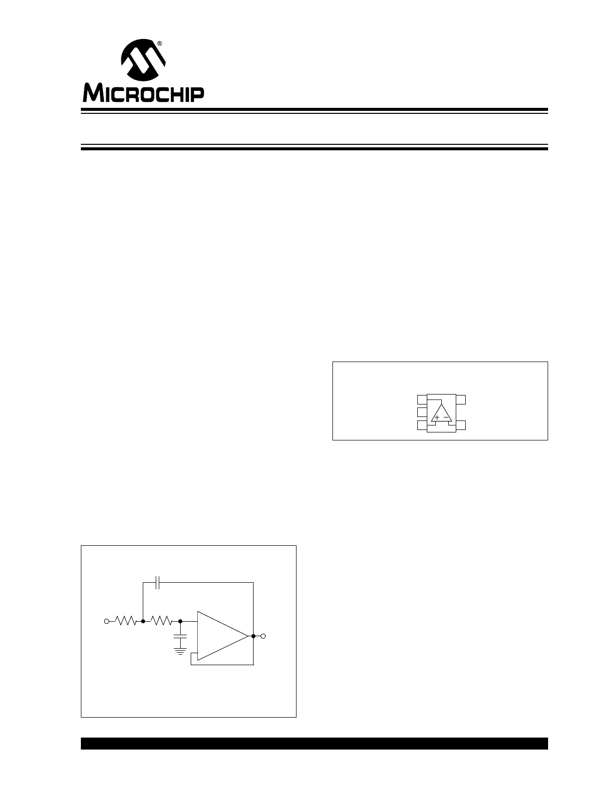
Typical Application
Description
The Microchip Technology Inc. MCP6286 operational
amplifier (op amp) has low noise (5.4 nV/
√Hz, typical),
low power (520 µA, typical) and rail-to-rail output
operation. It is unity gain stable and has a gain
bandwidth product of 3.5 MHz (typical). This device
operates with a single supply voltage as low as 2.2V,
while drawing low quiescent current. These features
make the product well suited for single-supply, low
noise, battery-powered applications.
The MCP6286 op amp is offered in a space saving
SOT-23-5 package. It is designed with Microchip’s
advanced CMOS process and available in the
extended temperature range, with a power supply
range of 2.2V to 5.5V.
Package Types
C
2
V
OUT
R
1
R
2
C
1
V
IN
47 nF
382 k
Ω 641 kΩ
22 nF
G = +1 V/V
f
P
= 10 Hz
+
–
MCP6286
Second-Order, Low-Pass Butterworth Filter
5
4
1
2
3
V
DD
V
IN–
V
IN+
V
SS
V
OUT
MCP6286
SOT-23-5
Low Noise, Low Power Op Amp

MCP6286
DS22196A-page 2
© 2009 Microchip Technology Inc.
NOTES:
© 2009 Microchip Technology Inc.
DS22196A-page 3
MCP6286
1.0
ELECTRICAL CHARACTERISTICS
1.1
Absolute Maximum Ratings †
V
DD
– V
SS
........................................................................7.0V
Current at Input Pins .....................................................±2 mA
Analog Inputs (V
IN
+
, V
IN
-
)†† .......... V
SS
– 1.0V to V
DD
+ 1.0V
All Other Inputs and Outputs ......... V
SS
– 0.3V to V
DD
+ 0.3V
Difference Input Voltage ...................................... |V
DD
– V
SS
|
Output Short-Circuit Current .................................continuous
Current at Output and Supply Pins ............................±30 mA
Storage Temperature ....................................-65°C to +150°C
Maximum Junction Temperature (T
J
) .......................... +150°C
ESD protection on all pins (HBM; MM)
................ ≥ 4 kV; 400V
† Notice: Stresses above those listed under “Absolute
Maximum Ratings” may cause permanent damage to the
device. This is a stress rating only and functional operation of
the device at those or any other conditions above those
indicated in the operational listings of this specification is not
implied. Exposure to maximum rating conditions for extended
periods may affect device reliability.
†† See
4.1.2 “Input Voltage And Current Limits”
DC ELECTRICAL SPECIFICATIONS
Electrical Characteristics: Unless otherwise indicated, V
DD
= +2.2V to +5.5V, V
SS
= GND, T
A
= +25°C, V
CM
= V
DD
/3,
V
OUT
≈ V
DD
/2, V
L
= V
DD
/2 and R
L
= 10 k
Ω to V
L
. (Refer to
Figure 1-1
).
Parameters
Sym
Min
Typ
Max
Units
Conditions
Input Offset
Input Offset Voltage
V
OS
-1.5
—
+1.5
mV
Input Offset Drift with Temperature
ΔV
OS
/
ΔT
A
—
±1
—
µV/°C T
A
= -40°C to +125°C
Power Supply Rejection Ratio
PSRR
80
100
—
dB
Input Bias Current and Impedance
Input Bias Current
I
B
—
±1
—
pA
—
50
150
pA
T
A
= +85°C
—
1500
3000
pA
T
A
= +125°C
Input Offset Current
I
OS
—
±1
—
pA
Common Mode Input Impedance
Z
CM
—
10
13
||20
—
Ω||pF
Differential Input Impedance
Z
DIFF
—
10
13
||20
—
Ω||pF
Common Mode
Common Mode Input Voltage
Range
V
CMR
V
SS
−0.3
—
V
DD
-1.2
V
Note 1
Common Mode Rejection Ratio
CMRR
76
95
—
dB
V
CM
= -0.3V to 1.0V,
V
DD
= 2.2V
80
100
—
dB
V
CM
= -0.3V to 4.3V,
V
DD
= 5.5V
Open-Loop Gain
DC Open-Loop Gain
(Large Signal)
A
OL
100
120
—
dB
0.2V < V
OUT
<(V
DD
-0.2V)
Output
Maximum Output Voltage Swing
V
OL,
V
OH
V
SS
+15
—
V
DD
–15
mV
0.5V Input overdrive
V
SS
+75
—
V
DD
–75
mV
0.5V Input overdrive
R
L
= 2 k
Ω
Output Short-Circuit Current
I
SC
—
±20
—
mA
Note 1:
Figure 2-12
shows how V
CMR
changes across temperature.
MCP6286
DS22196A-page 4
© 2009 Microchip Technology Inc.
Power Supply
Supply Voltage
V
DD
2.2
—
5.5
V
Quiescent Current per Amplifier
I
Q
300
520
700
µA
I
O
= 0, V
DD
= 2.2V
320
540
720
µA
I
O
= 0, V
DD
= 5.5V
DC ELECTRICAL SPECIFICATIONS (CONTINUED)
Electrical Characteristics: Unless otherwise indicated, V
DD
= +2.2V to +5.5V, V
SS
= GND, T
A
= +25°C, V
CM
= V
DD
/3,
V
OUT
≈ V
DD
/2, V
L
= V
DD
/2 and R
L
= 10 k
Ω to V
L
. (Refer to
Figure 1-1
).
Parameters
Sym
Min
Typ
Max
Units
Conditions
Note 1:
Figure 2-12
shows how V
CMR
changes across temperature.
AC ELECTRICAL SPECIFICATIONS
Electrical Characteristics: Unless otherwise indicated, T
A
= +25°C, V
DD
= +2.2 to +5.5V, V
SS
= GND, V
CM
= V
DD
/3,
V
OUT
≈ V
DD
/2, V
L
= V
DD
/2, R
L
= 10 k
Ω to V
L
and C
L
= 60 pF. (Refer to
Figure 1-1
).
Parameters
Sym
Min
Typ
Max
Units
Conditions
AC Response
Gain Bandwidth Product
GBWP
—
3.5
—
MHz
Phase Margin
PM
—
60
—
°
G = +1 V/V
Slew Rate
SR
—
2
—
V/µs
Noise
Input Noise Voltage
E
ni
—
1.0
—
µV
P-P
f = 0.1 Hz to 10 Hz
Input Noise Voltage Density
e
ni
—
22
—
nV/
√Hz f = 10 Hz
—
5.4
—
nV/
√Hz f = 10 kHz
Input Noise Current Density
i
ni
—
0.6
—
fA/
√Hz f = 1 kHz
TEMPERATURE SPECIFICATIONS
Electrical Characteristics: Unless otherwise indicated, V
DD
= +2.2V to +5.5V and V
SS
= GND.
Parameters
Sym
Min
Typ
Max
Units
Conditions
Temperature Ranges
Operating Temperature Range
T
A
-40
—
+125
°C
Note 1
Storage Temperature Range
T
A
-65
—
+150
°C
Thermal Package Resistances
Thermal Resistance, 5L-SOT-23
θ
JA
—
256
—
°C/W
Note 1: The internal junction temperature (T
J
) must not exceed the absolute maximum specification of +150°C.
© 2009 Microchip Technology Inc.
DS22196A-page 5
MCP6286
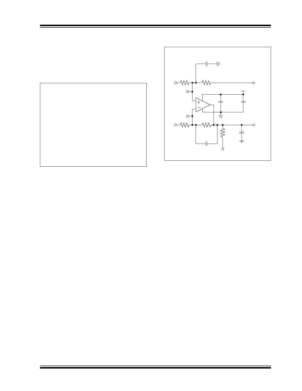
1.2
Test Circuits
The circuit used for most DC and AC tests is shown in
Figure 1-1
. It independently sets V
CM
and V
OUT
; see
Equation 1-1
. The circuit’s common mode voltage is
(V
P
+ V
M
)/2, not V
CM
. V
OST
includes V
OS
plus the
effects of temperature, CMRR, PSRR and A
OL
.
EQUATION 1-1:
FIGURE 1-1:
AC and DC Test Circuit for
Most Specifications.
G
DM
R
F
R
G
⁄
=
V
CM
V
P
1
1 G
N
⁄
–
(
) V
REF
1 G
N
⁄
(
)
+
=
V
OUT
V
REF
V
P
V
M
–
(
)G
DM
V
OST
G
N
+
+
=
Where:
G
DM
= Differential Mode Gain
(V/V)
G
N
= Noise Gain
(V/V)
V
CM
= Op Amp’s Common Mode
Input Voltage
(V)
V
OST
= Op Amp’s Total Input Offset
Voltage
(mV)
V
OST
V
IN–
V
IN+
–
=
G
N
1
G
DM
+
=
V
DD
MCP6286
R
G
R
F
V
OUT
V
M
C
B2
C
L
R
L
V
L
C
B1
100 k
Ω
100 k
Ω
R
G
R
F
V
REF
= V
DD
/2
V
P
100 k
Ω
100 k
Ω
60 pF
10 k
Ω
1 µF
100 nF
V
IN–
V
IN+
C
F
6.8 pF
C
F
6.8 pF

MCP6286
DS22196A-page 6
© 2009 Microchip Technology Inc.
NOTES:
© 2009 Microchip Technology Inc.
DS22196A-page 7
MCP6286
2.0
TYPICAL PERFORMANCE CURVES
Note: Unless otherwise indicated, T
A
= +25°C, V
DD
= +2.2V to +5.5V, V
SS
= GND, V
CM
= V
DD
/3, V
OUT
≈ V
DD
/2,
V
L
= V
DD
/2, R
L
= 10 k
Ω to V
L
and C
L
= 60 pF.
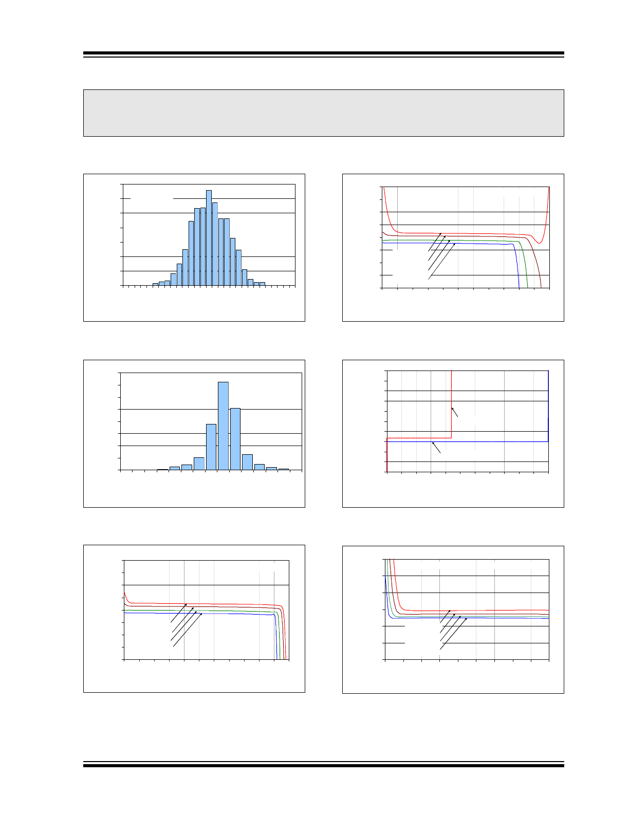
FIGURE 2-1:
Input Offset Voltage.
FIGURE 2-2:
Input Offset Voltage Drift.
FIGURE 2-3:
Input Offset Voltage vs.
Common Mode Input Voltage with V
DD
= 5.5V.
FIGURE 2-4:
Input Offset Voltage vs.
Common Mode Input Voltage with V
DD
= 2.2V.
FIGURE 2-5:
Input Offset Voltage vs.
Output Voltage.
FIGURE 2-6:
Input Offset Voltage vs.
Power Supply Voltage with V
CM
= V
CMR_L
.
Note:
The graphs and tables provided following this note are a statistical summary based on a limited number of
samples and are provided for informational purposes only. The performance characteristics listed herein
are not tested or guaranteed. In some graphs or tables, the data presented may be outside the specified
operating range (e.g., outside specified power supply range) and therefore outside the warranted range.
0%
2%
4%
6%
8%
10%
12%
14%
-8
00
-6
00
-5
00
-4
00
-3
00
-2
00
-1
00
0
10
0
20
0
30
0
40
0
50
0
60
0
80
0
Input Offset Voltage (µV)
Percentage of
Oc
cu
rrenc
es
1360 Samples
0%
5%
10%
15%
20%
25%
30%
35%
40%
-3
.5
-3
.0
-2
.5
-2
.0
-1
.5
-1
.0
-0
.5
0.
0
0.
5
1.
0
1.
5
2.
0
2.
5
3.
0
3.
5
Input Offset Drift with Temperature (µV/°C)
P
e
rc
entag
e
of Occ
u
rrenc
es
1360 Samples
-800
-600
-400
-200
0
200
400
600
800
-0.5 0.0 0.5 1.0 1.5 2.0 2.5 3.0 3.5 4.0 4.5 5.0
Common Mode Input Voltage (V)
In
p
u
t
O
ff
s
e
t V
o
lt
ag
e (
µ
V
)
T
A
= +125
°C
T
A
= +85°C
T
A
= +25°C
T
A
= -40°C
Representative Part
V
DD
= 5.5V
-800
-600
-400
-200
0
200
400
600
800
-0
.5
-0
.3
-0
.1
0.
1
0.
3
0.
5
0.
7
0.
9
1.
1
1.
3
1.
5
1.
7
Common Mode Input Voltage (V)
In
p
u
t O
ff
s
et
V
o
lt
ag
e
(µ
V)
T
A
= +125°C
T
A
= +85°C
T
A
= +25°C
T
A
= -40°C
Representative Part
V
DD
= 2.2V
-500
-400
-300
-200
-100
0
100
200
300
400
500
0.0
0.5
1.0
1.5
2.0
2.5
3.0
3.5
4.0
4.5
5.0
5.5
Output Voltage (V)
Input Of
fset
V
o
lt
age
(µV
)
V
DD
= 2.2V
V
DD
= 5.5V
-600
-400
-200
0
200
400
600
1.5
2.0
2.5
3.0
3.5
4.0
4.5
5.0
5.5
6.0
Power Supply Voltage (V)
In
p
u
t O
ffs
e
t V
o
lt
a
g
e
(µ
V
)
V
CM
= V
CMR-L
Representative Part
T
A
= +125°C
T
A
= +85°C
T
A
= +25°C
T
A
= -40°C
MCP6286
DS22196A-page 8
© 2009 Microchip Technology Inc.
Note: Unless otherwise indicated, T
A
= +25°C, V
DD
= +2.2V to +5.5V, V
SS
= GND, V
CM
= V
DD
/3, V
OUT
≈ V
DD
/2,
V
L
= V
DD
/2, R
L
= 10 k
Ω to V
L
and C
L
= 60 pF.
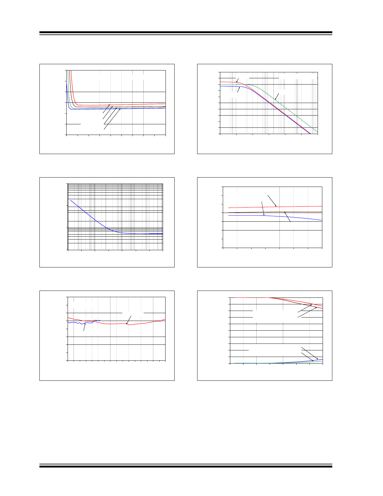
FIGURE 2-7:
Input Offset Voltage vs.
Power Supply Voltage with V
CM
= V
CMR_H
.
FIGURE 2-8:
Input Noise Voltage Density
vs. Frequency.
FIGURE 2-9:
Input Noise Voltage Density
vs. Common Mode Input Voltage.
FIGURE 2-10:
CMRR, PSRR vs.
Frequency.
FIGURE 2-11:
CMRR, PSRR vs. Ambient
Temperature.
FIGURE 2-12:
Common Mode Input
Voltage Headroom vs. Ambient Temperature.
-600
-400
-200
0
200
400
600
1.5 2.0 2.5 3.0 3.5 4.0 4.5 5.0 5.5 6.0
Power Supply Voltage (V)
Input Of
fset
V
o
lt
age (µV)
V
CM
= V
CMR-H
Representative Part
T
A
= +125°C
T
A
= +85°C
T
A
= +25°C
T
A
= -40°C
1
10
100
1,000
1.E-1 1.E+0 1.E+1 1.E+2 1.E+3 1.E+4 1.E+5 1.E+6
Frequency (Hz)
Input Noise Voltage Den
s
ity
(n
V
/√
Hz)
0.1 1 10 100 1k 10k 100k 1M
3.0
3.5
4.0
4.5
5.0
5.5
6.0
6.5
7.0
-0
.3
0.0
0.3
0.6
0.9
1.2
1.5
1.8
2.1
2.4
2.7
3.0
3.3
3.6
3.9
4.2
4.5
Common Mode Input Voltage (V)
Inpu
t V
o
lta
g
e No
ise
Dens
ity
(nV
/√
Hz)
V
DD
= 5.5 V
V
DD
= 2.2 V
f = 10 kHz
20
30
40
50
60
70
80
90
100
110
120
1
10
100
1000
10000 100000 1E+06
Frequency (Hz)
CM
RR,
P
S
R
R
(d
B)
Representative Part
CMRR
PSRR+
PSRR-
1
10
100
1k
10k
100k
1M
75
80
85
90
95
100
105
110
-50
-25
0
25
50
75
100
125
Ambient Temperature (°C)
CM
RR,
P
S
RR
(
d
B)
PSRR
CMRR @ V
DD
= 5.5V
@ V
DD
= 2.2V
-0.30
-0.15
0.00
0.15
0.30
0.45
0.60
0.75
0.90
1.05
1.20
-50
-25
0
25
50
75
100
125
Ambient Temperature (°C)
Comm
on M
ode Input Voltage
Headro
om (
V
)
V
CMR_L
- V
SS
@ V
DD
= 2.2V
V
OL
- V
SS
@ V
DD
= 5.5V
V
V
V
DD
- V
CMR_H
@ V
DD
= 5.5V
@ V
DD
= 2.2V
© 2009 Microchip Technology Inc.
DS22196A-page 9
MCP6286
Note: Unless otherwise indicated, T
A
= +25°C, V
DD
= +2.2V to +5.5V, V
SS
= GND, V
CM
= V
DD
/3, V
OUT
≈ V
DD
/2,
V
L
= V
DD
/2, R
L
= 10 k
Ω to V
L
and C
L
= 60 pF.
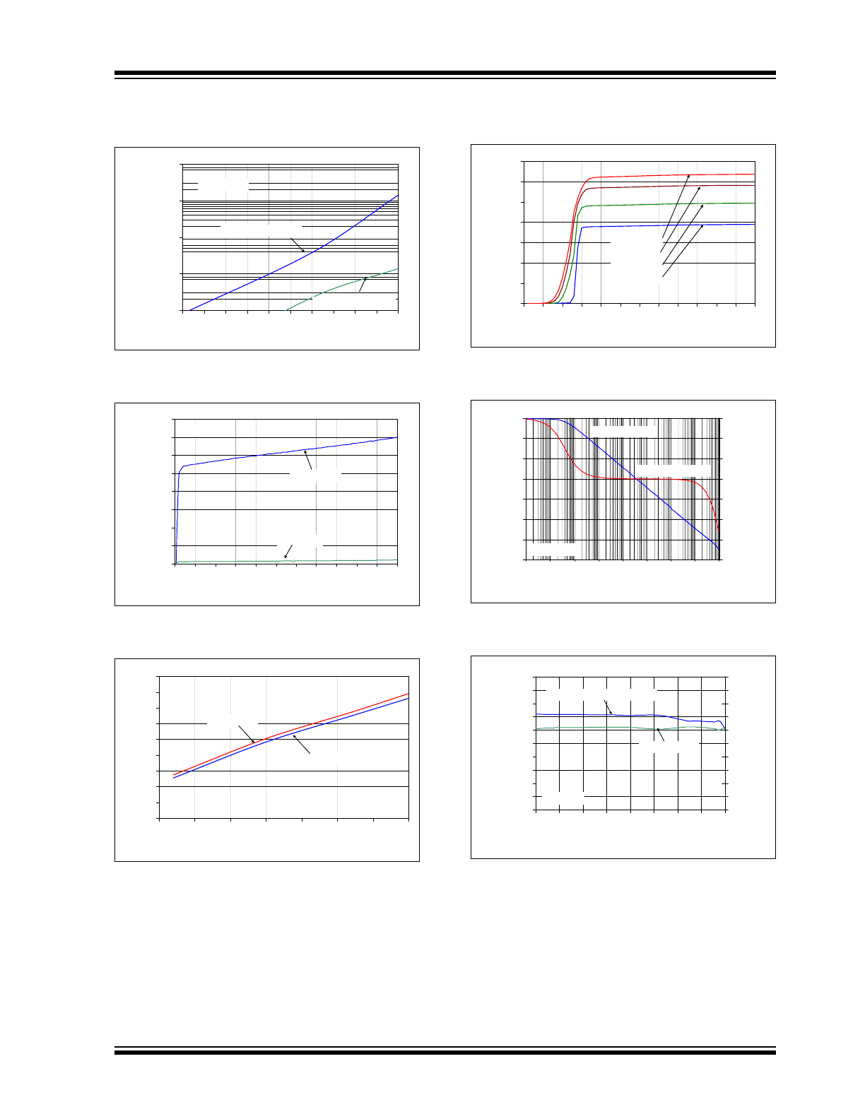
FIGURE 2-13:
Input Bias, Offset Currents
vs. Ambient Temperature.
FIGURE 2-14:
Input Bias Current vs.
Common Mode Input Voltage.
FIGURE 2-15:
Quiescent Current vs
Ambient Temperature.
FIGURE 2-16:
Quiescent Current vs.
Power Supply Voltage.
FIGURE 2-17:
Open-Loop Gain, Phase vs.
Frequency.
FIGURE 2-18:
Gain Bandwidth Product,
Phase Margin vs. Common Mode Input Voltage
with V
DD
= 5.5V.
1
10
100
1000
10000
25 35 45 55 65 75 85 95 105 115 125
Ambient Temperature (°C)
Input
B
ias, Of
fset
Current
s (
p
A)
Input Bias Current
Input Offset Current
V
DD
= 5.5V
0
200
400
600
800
1000
1200
1400
1600
0.0 0.5 1.0 1.5 2.0 2.5 3.0 3.5 4.0 4.5 5.0 5.5
Common Mode Input Votlage (V)
In
p
u
t Bi
a
s
Cu
rr
e
n
t (p
A)
V
DD
= 5.5V
T
A
= +125°C
T
A
= +85°C
250
300
350
400
450
500
550
600
650
700
-50
-25
0
25
50
75
100
125
Ambient Temperature (°C)
Q
u
ie
sc
ent
Cur
re
nt (
µ
A)
V
DD
= 5.5V
V
DD
= 2.2V
0
100
200
300
400
500
600
700
0.0
0.5
1.0
1.5
2.0
2.5
3.0
3.5
4.0
4.5
5.0
5.5
6.0
Power Supply Voltage (V)
Q
u
ie
sc
ent Cur
re
nt (
u
A)
T
A
= +125°C
T
A
= +85°C
T
A
= +25°C
T
A
= -40°C
-20
0
20
40
60
80
100
120
1.0E-01
1.0E+00
1.0E+01
1.0E+02
1.0E+03
1.0E+04
1.0E+05
1.0E+06
1.0E+07
Frequency (Hz)
O
p
e
n
-L
oo
p
G
a
in
(d
B)
-210
-180
-150
-120
-90
-60
-30
0
O
p
en
-L
o
o
p
P
h
as
e
(°
)
Open-Loop Gain
Open-Loop Phase
V
DD
= 5.5V
0.1
1
10 100
1k 10k 100k 1M 10M
0.0
0.5
1.0
1.5
2.0
2.5
3.0
3.5
4.0
4.5
5.0
-0
.4
0.
2
0.
8
1.
4
2.
0
2.
6
3.
2
3.
8
4.
4
Common Mode Input Voltage (V)
Ga
in
B
a
n
d
wi
d
th
P
ro
d
u
c
t
(M
H
z)
0
10
20
30
40
50
60
70
80
90
100
Ph
as
e (
°)
Phase Margin
Gain Bandwidth Product
V
DD
= 5.5V
MCP6286
DS22196A-page 10
© 2009 Microchip Technology Inc.
Note: Unless otherwise indicated, T
A
= +25°C, V
DD
= +2.2V to +5.5V, V
SS
= GND, V
CM
= V
DD
/3, V
OUT
≈ V
DD
/2,
V
L
= V
DD
/2, R
L
= 10 k
Ω to V
L
and C
L
= 60 pF
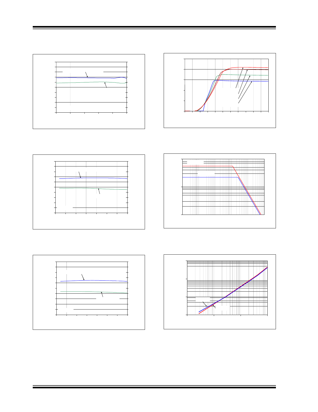
FIGURE 2-19:
Gain Bandwidth Product,
Phase Margin vs. Common Mode Input Voltage
with V
DD
= 2.2V.
FIGURE 2-20:
Gain Bandwidth Product,
Phase Margin vs. Ambient Temperature with
V
DD
= 5.5V.
FIGURE 2-21:
Gain Bandwidth Product,
Phase Margin vs. Ambient Temperature with
V
DD
= 2.2V.
FIGURE 2-22:
Ouput Short Circuit Current
vs. Power Supply Voltage.
FIGURE 2-23:
Output Voltage Swing vs.
Frequency.
FIGURE 2-24:
Output Voltage Headroom
vs. Output Current.
0.0
0.5
1.0
1.5
2.0
2.5
3.0
3.5
4.0
4.5
5.0
-0.4
-0.1
0.2
0.5
0.8
1.1
Common Mode Input Voltage (V)
G
a
in
B
a
ndw
id
th
P
rod
u
c
t
(M
H
z)
0
10
20
30
40
50
60
70
80
90
100
Ph
as
e (
°)
Phase Margin
Gain Bandwidth Product
V
DD
= 2.2V
0.0
0.5
1.0
1.5
2.0
2.5
3.0
3.5
4.0
4.5
5.0
-50
-25
0
25
50
75
100
125
Ambient Temperature (°C)
G
a
in
B
a
n
d
w
id
th
P
rod
u
c
t
(M
H
z)
40
45
50
55
60
65
70
75
80
85
90
P
h
as
e (°
)
Gain Bandwidth Product
Phase Margin
V
DD
= 5.5V
0.0
0.5
1.0
1.5
2.0
2.5
3.0
3.5
4.0
4.5
5.0
-50
-25
0
25
50
75
100
125
Ambient Temperature (°C)
G
a
in
B
a
nd
w
id
th
P
ro
d
uc
t
(M
H
z)
40
45
50
55
60
65
70
75
80
85
90
Ph
as
e (
°)
Gain Bandwidth Product
Phase Margin
V
DD
= 2.2V
0
5
10
15
20
25
0.
0
0.
5
1.
0
1.
5
2.
0
2.
5
3.
0
3.
5
4.
0
4.
5
5.
0
5.
5
Power Supply Voltage (V)
Output
S
h
ort
Circuit
C
u
rrent
(mA
)
T
A
= +125°C
T
A
= +85°C
T
A
= +25°C
T
A
= -40°C
0.1
1
10
100
1000
10000
100000
1000000
10000000
Frequency (Hz)
Output
V
o
ltage Swing (V
P-P
)
V
DD
= 2.2V
V
DD
= 5.5V
100 1k 10k 100k 1M 10M
1
10
100
1000
0.01
0.1
1
10
Output Current (mA)
Output
V
o
lt
age Headroom
(mV)
V
OL
- V
SS
V
DD
- V
OH