
2002 Microchip Technology Inc.
DS21344B-page 1
Features
• Tiny SOT-23A Packages
• Optimized for Single Supply Operation
• Ultra Low Input Bias Current: Less than 100pA
• Low Quiescent Current: 4
µ
A (TC1037),
Shutdown Mode: 4
µ
A, 0.05
µ
A (TC1038),
6
µ
A (TC1039)
• Shutdown Mode (TC1038)
• 2.0% Accurate Independent Voltage Reference
(TC1039)
• Rail-to-Rail Inputs and Outputs
• Operation Down to V
DD
= 1.8V
Applications
• Power Management Circuits
• Battery Operated Equipment
• Consumer Products
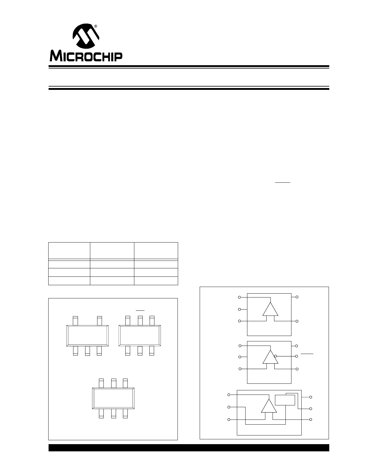
Device Selection Table
Package Types
General Description
The TC1037/TC1038/TC1039 are single, low-power
comparators designed for low-power applications.
These comparators are specifically designed for
operation from a single supply. However, operation
from dual supplies also is possible, and power supply
current is independent of the magnitude of the power
supply voltage. The TC1037/TC1038/TC1039 operate
from two 1.5V alkaline cells down to V
DD
= 1.8V. Active
supply current is 4
µ
A for the TC1037/TC1038 and 6
µ
A
for the TC1039. Input and output swing of these
devices is rail-to-rail.
An active low shutdown input, SHDN, is available on
the TC1038 and disables the comparator, placing its
output in a high-impedance state. The TC1038 draws
only 0.05
µ
A (typical) when the shutdown mode is
active.
An internally biased 1.20V bandgap reference is
included in the TC1039. The reference is accurate to
2.0 percent tolerance. This reference is independent of
the comparator in the TC1039.
Packaged in a 5-Pin SOT-23A (TC1037) or 6-Pin
SOT-23A (TC1038/TC1039), these single comparators
are ideal for applications requiring high integration,
small size and low power.
Functional Block Diagram
Part Number
Package
Temperature
Range
TC1037CECT
5-Pin SOT-23A
-40°C to +85°C
TC1038CECH
6-Pin SOT-23A
-40°C to +85°C
TC1039CECH
6-Pin SOT-23A
-40°C to +85°C
OUTPUT
V
SS
IN+
V
DD
IN-
5-Pin SOT-23A
TC1037ECT
1
3
5
4
2
OUTPUT
V
SS
IN+
V
DD
IN-
SHDN
6-Pin SOT-23A
TC1038ECH
1
3
6
4
5
2
OUTPUT
V
SS
IN+
V
DD
IN-
REF
6-Pin SOT-23A
TC1039ECH
1
3
6
4
5
2
NOTE: 5-Pin SOT-23A is equivalent to the EIAJ SC-74A.
6-Pin SOT-23A is equivalent to the EIAJ SC-74.
+
–
OUTPUT
IN+
TC1037
+
–
OUTPUT
IN+
TC1038
1
2
3
5
4
6
5
4
1
2
3
6
5
4
2
3
V
SS
V
DD
IN-
V
DD
SHDN
IN-
V
SS
1
+
–
OUTPUT
IN+
TC1039
V
SS
Voltage
Reference
V
DD
IN-
REF
TC1037/TC1038/TC1039
Linear Building Block – Single Comparator in SOT Packages
TC1037/TC1038/TC1039
DS21344B-page 2
2002 Microchip Technology Inc.
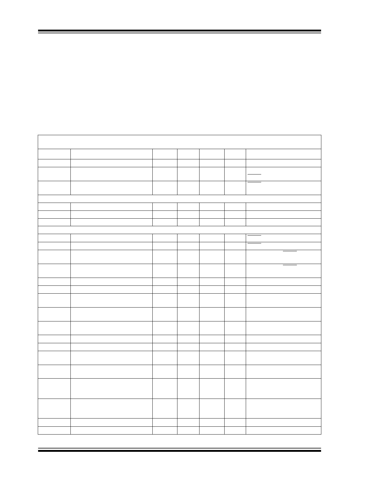
1.0
ELECTRICAL
CHARACTERISTICS
ABSOLUTE MAXIMUM RATINGS*
Supply Voltage ......................................................6.0V
Voltage on Any Pin .......... (V
SS
– 0.3V) to (V
DD
+ 0.3V)
Junction Temperature....................................... +150°C
Operating Temperature Range............. -40°C to +85°C
Storage Temperature Range .............. -55°C to +150°C
*Stresses above those listed under "Absolute Maximum
Ratings" may cause permanent damage to the device. These
are stress ratings only and functional operation of the device
at these or any other conditions above those indicated in the
operation sections of the specifications is not implied.
Exposure to Absolute Maximum Rating conditions for
extended periods may affect device reliability.
TC1037/TC1038/TC1039 ELECTRICAL SPECIFICATIONS
Electrical Characteristics: Typical values apply at 25°C and V
DD
= 3.0V. Minimum and maximum values apply for T
A
= -40° to
+85°C and V
DD
= 1.8V to 5.5V, unless otherwise specified.
Symbol
Parameter
Min
Typ
Max
Units
Test Conditions
V
DD
Supply Voltage
1.8
—
5.5
V
I
Q
Supply Current, Operating (TC1039)
(TC1037/TC1038)
—
—
6
4
10
8
µ
A
µ
A
All Outputs Unloaded,
SHDN = V
DD
for TC1038
I
SHDN
Supply Current Shutdown Mode
(TC1038 Only)
—
—
0.3
µ
A
SHDN = V
SS
Shutdown Input (TC1038 Only)
V
IH
Input High Threshold
80% V
DD
—
—
V
V
IL
Input Low Threshold
—
—
20% V
DD
V
I
SI
Shutdown Input Current
—
—
±100
nA
Comparator
R
OUT
(SD)
Output Resistance in Shutdown
20
—
—
M
Ω
SHDN = V
SS
(TC1038 Only)
C
OUT
(SD)
Output Capacitance in Shutdown
—
—
5
pF
SHDN = V
SS
(TC1038 Only)
T
SEL
Select Time
—
20
—
µ
sec
V
OUT
Valid from SHDN = V
IH
R
L
= 10k
Ω
to V
SS
(TC1038 Only)
T
DESEL
Deselect Time
—
500
—
nsec
V
OUT
Valid from SHDN = V
IL
R
L
= 10k
Ω
to V
SS
V
ICMR
Common Mode Input Voltage Range V
SS
– 0.2
—
V
DD
+ 0.2
V
A
VOL
Large Signal Voltage Gain
—
100
—
V/mV
R
L
= 10k
Ω
, V
DD
= 5V
GBWP
Gain Bandwidth Product
—
90
—
kHz
V
DD
= 1.8V to 5.5V;
V
O
= V
DD
to V
SS
V
OS
Input Offset Voltage
–5
–5
—
+5
+5
mV
mV
V
DD
= 3V, V
CM
= 1.5V, T
A
= 25°C,
T
A
= -40°C to 85°C
I
B
Input Bias Current
—
—
±100
pA
T
A
= 25°C;
IN+, IN- = V
DD
to V
SS
V
OH
Output High Voltage
V
DD
– 0.3
—
—
V
R
L
= 10k
Ω
to V
SS
V
OL
Output Low Voltage
—
—
0.3
V
R
L
= 10k
Ω
to V
DD
CMRR
Common Mode Rejection Ratio
66
—
—
dB
T
A
= 25°C; V
DD
= 5V;
V
CM
= V
DD
to V
SS
PSRR
Power Supply Rejection Ratio
60
—
—
dB
T
A
= 25°C; V
CM
= 1.2V;
V
DD
= 1.8V to 5V
I
SRC
Output Source Current
1
—
—
mA
IN+ = V
DD
, IN- = V
SS
Output Shorted to V
SS
V
DD
= 1.8V
I
SINK
Output Sink Current
2
—
—
mA
IN+ = V
SS
, IN- = V
SS
Output Shorted to V
SS
V
DD
= 1.8V
T
PD1
Response Time
—
4
—
µ
sec
100mV Overdrive, C
L
= 100pF
T
PD2
Response Time
—
6
—
µ
sec
10mV Overdrive, C
L
= 100pF
2002 Microchip Technology Inc.
DS21344B-page 3
TC1037/TC1038/TC1039
TC1037/TC1038/TC1039 ELECTRICAL SPECIFICATIONS (CONTINUED)
Electrical Characteristics: Typical values apply at 25°C and V
DD
= 3.0V. Minimum and maximum values apply for T
A
= -40° to
+85°C and V
DD
= 1.8V to 5.5V, unless otherwise specified.
Symbol
Parameter
Min
Typ
Max
Units
Test Conditions
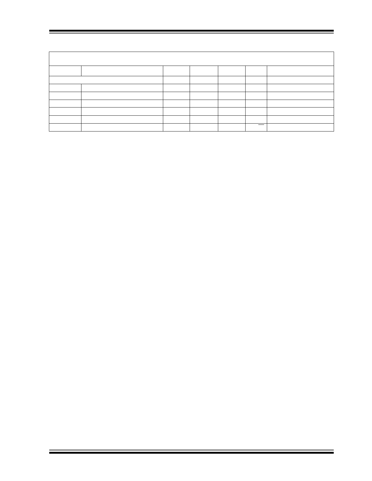
Voltage Reference (TC1039 Only)
V
REF
Reference Voltage
1.176
1.200
1.224
V
I
REF(SOURCE)
Source Current
50
—
—
µ
A
I
REF(SINK)
Sink Current
50
—
—
µ
A
C
L(REF)
Load Capacitance
—
—
100
pF
E
VREF
Noise Voltage
—
20
—
µ
V
RMS
100Hz to 100kHz
e
VREF
Noise Voltage Density
—
1.0
—
µ
V/
√
Hz 1kHz
TC1037/TC1038/TC1039
DS21344B-page 4
2002 Microchip Technology Inc.
2.0
PIN DESCRIPTIONS
The description of the pins are listed in Table 2-1.
TABLE 2-1:
PIN FUNCTION TABLE
Pin No.
TC1037
(5-Pin SOT-23A)
Symbol
Description
1
OUTPUT
Comparator output.
2
V
SS
Negative power supply.
3
IN+
Comparator non-inverting input.
4
IN-
Comparator inverting input.
5
V
DD
Positive power supply.
Pin No.
TC1038
(6-Pin SOT-23A)
Symbol
Description
1
OUTPUT
Comparator output.
2
V
SS
Negative power supply.
3
IN+
Comparator non-inverting input.
4
IN-
Comparator inverting input.
5
SHDN
Active low shutdown input (TC1038 only). A low input on this pin disables the comparator
and places the output terminal in a high impedance state.
6
V
DD
Positive power supply.
Pin No.
TC1039
(6-Pin SOT-23A)
Symbol
Description
1
OUTPUT
Comparator output.
2
V
SS
Negative power supply.
3
IN+
Comparator non-inverting input.
4
IN-
Comparator inverting input.
5
REF
1.20V bandgap voltage reference output (TC1039 only).
6
V
DD
Positive power supply.

2002 Microchip Technology Inc.
DS21344B-page 5
TC1037/TC1038/TC1039
3.0
DETAILED DESCRIPTION
The TC1037/TC1038/TC1039 are a series of very low
power, linear building block products targeted at low
voltage, single supply applications. The TC1037/
TC1038/TC1039 minimum operating voltage is 1.8V
and typical supply current is only 4
µ
A for the TC1037
and TC1038 (fully enabled) and 6
µ
A for the TC1039.
3.1
Comparator
The
TC1037/8/9
contain
one
comparator.
The
comparator’s input range extends beyond both supply
voltages by 200mV and the outputs will swing to within
several millivolts of the supplies depending on the load
current being driven.
The comparator exhibits a propagation delay and
supply current which is largely independent of supply
voltage. The low input bias current and offset voltage
makes it suitable for high impedance precision
applications.
The TC1038 comparator is disabled during shutdown
and has a high impedance output.
3.2
Voltage Reference
A 2.0% tolerance, internally biased, 1.20V bandgap
voltage reference is included in the TC1039. It has a
push-pull output capable of sourcing and sinking at
least 50
µ
A.
3.3
Shutdown Input (TC1038 Only)
SHDN at V
IL
disables the comparator and reduces the
supply current to less than 0.3
µ
A. The SHDN input
cannot be allowed to float. When not used, connect it to
V
DD
. The comparator’s output is in a high impedance
state when the TC1038 is disabled. The comparator’s
inputs can be driven from rail-to-rail by an external
voltage when the TC1038 is disabled. No latchup will
occur when the device is driven to its enabled state
when SHDN is set to V
IH
.
4.0
TYPICAL APPLICATIONS
The TC1037/TC1038/TC1039 family lends itself to a
wide variety of applications, particularly in battery
powered systems. It typically finds application in power
management, processor supervisory and interface
circuitry.
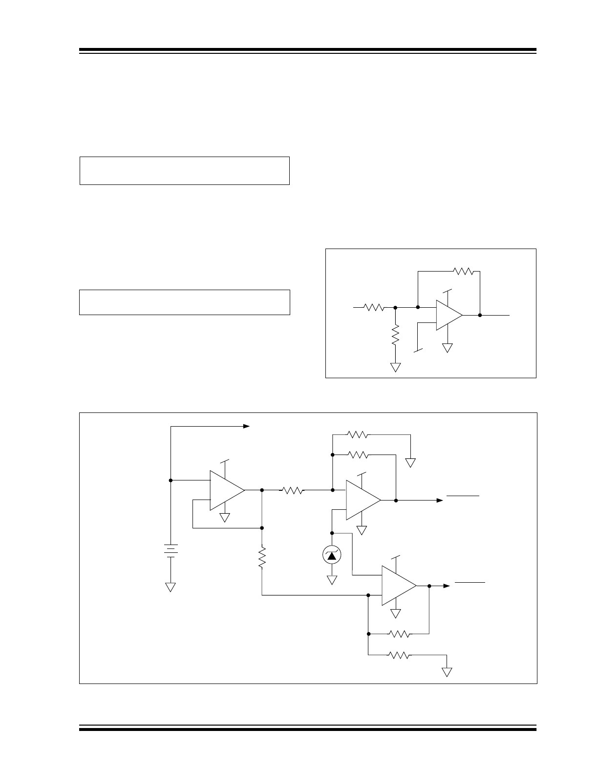
4.1
External Hysteresis (Comparator)
Hysteresis can be set externally with two resistors
using positive feedback techniques (see Figure 4-1).
The design procedure for setting external comparator
hysteresis is as follows:
1.
Choose the feedback resistor R
C
. Since the
input bias current of the comparator is at most
100pA, the current through R
C
can be set to
100nA (i.e., 1000 times the input bias current)
and retain excellent accuracy. The current
through R
C
at the comparator’s trip point is V
R
/
R
C
where V
R
is a stable reference voltage.
2.
Determine the hysteresis voltage (V
HY
) between
the upper and lower thresholds.
3.
Calculate R
A
as follows:
EQUATION 4-1:
4.
Choose the rising threshold voltage for V
SRC
(V
THR
).
5.
Calculate R
B
as follows:
EQUATION 4-2:
6.
Verify
the
threshold
voltages
with
these
formulas:
V
SRC
rising:
EQUATION 4-3:
V
SRC
falling:
EQUATION 4-4:
R
A
R
C
V
HY
V
DD
-----------
=
R
B
1
V
THR
V
R
R
A
×
---------------------
1
R
A
-------
–
1
R
C
-------
–
-----------------------------------------------------------
=
V
TH R
V
R
(
)
R
A
(
)
1
R
A
-------
1
R
B
-------
1
R
C
-------
+
+
=
V
THF
V
THR
R
A
V
DD
×
R
C
-------------------------
–
=

TC1037/TC1038/TC1039
DS21344B-page 6
2002 Microchip Technology Inc.
4.2
Precision Battery Monitor
Figure 4-2 is a precision battery low/battery dead
monitoring circuit. Typically, the battery low output
warns the user that a battery dead condition is
imminent. Battery dead typically initiates a forced
shutdown to prevent operation at low internal supply
voltages (which can cause unstable system operation).
The circuit in Figure 4-2 uses a TC1034, a TC1037 and
a TC1039, and only six external resistors. AMP 1 is a
simple buffer, while CMPTR1 and CMPTR2 provide
precision voltage detection using V
R
as a reference.
Resistors R2 and R4 set the detection threshold for
BATT LOW, while resistors R1 and R3 set the detection
threshold for BATT FAIL. The component values shown
assert BATT LOW at 2.2V (typical) and BATT FAIL at
2.0V (typical). Total current consumed by this circuit is
typically 16
µ
A at 3V. Resistors R5 and R6 provide
hysteresis for comparators CMPTR1 and CMPTR2,
respectively.
4.3
32.768 kHz “Time Of Day Clock”
Crystal Controlled Oscillator
A very stable oscillator driver can be designed by using
a crystal resonator as the feedback element. Figure 4-3
shows a typical application circuit using this technique
to develop a clock driver for a Time Of Day (TOD) clock
chip. The value of R
A
and R
B
determine the DC voltage
level at which the comparator trips – in this case one-
half of V
DD
. The RC time constant of R
C
and C
A
should
be set several times greater than the crystal oscillator’s
period, which will ensure a 50% duty cycle by maintain-
ing a DC voltage at the inverting comparator input
equal to the absolute average of the output signal.
4.4
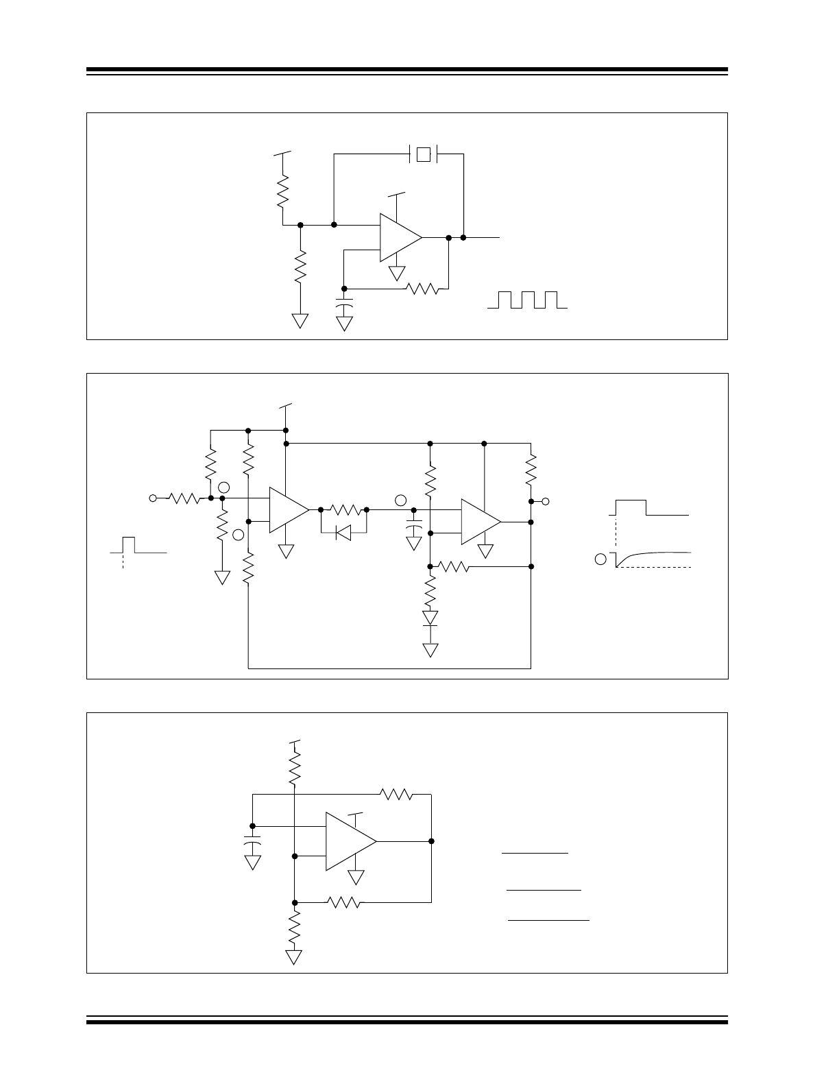
Non-Retriggerable One Shot
Multivibrator
Using two comparators, a non-retriggerable one shot
multivibrator can be designed using the circuit configu-
ration of Figure 4-4. A key feature of this design is that
the pulse width is independent of the magnitude of the
supply voltage because the charging voltage and the
intercept voltage are a fixed percentage of V
DD
. In
addition, this one shot is capable of pulse width with as
much as a 99% duty cycle and exhibits input lockout to
ensure that the circuit will not re-trigger before the
output pulse has completely timed out. The trigger level
is the voltage required at the input to raise the voltage
at node A higher than the voltage at node B, and is set
by the resistive divider R4 and R10 and the impedance
network composed of R1, R2 and R3. When the one
shot has been triggered, the output of CMPTR2 is high,
causing the reference voltage at the non-inverting input
of CMPTR1 to go to V
DD
. This prevents any additional
input pulses from disturbing the circuit until the output
pulse has timed out.
The value of the timing capacitor C1 must be small
enough to allow CMPTR1 to discharge C1 to a diode
voltage before the feedback signal from CMPTR2
(through R10) switches CMPTR1 to its high state and
allows C1 to start an exponential charge through R5.
Proper circuit action depends upon rapidly discharging
C1 through the voltage set by R6, R9 and D2 to a final
voltage of a small diode drop. Two propagation delays
after the voltage on C1 drops below the level on the
non-inverting input of CMPTR2, the output of CMPTR1
switches to the positive rail and begins to charge C1
through R5. The time delay which sets the output pulse
width results from C1 charging to the reference voltage
set by R6, R9 and D2, plus four comparator propaga-
tion delays. When the voltage across C1 charges
beyond the reference, the output pulse returns to
ground and the input is again ready to accept a trigger
signal.
4.5
Oscillators and Pulse Width
Modulators
Microchip’s linear building block comparators adapt
well to oscillator applications for low frequencies (less
than 100kHz). Figure 4-5 shows a symmetrical square
wave generator using a minimum number of compo-
nents. The output is set by the RC time constant of R4
and C1, and the total hysteresis of the loop is set by R1,
R2 and R3. The maximum frequency of the oscillator is
limited only by the large signal propagation delay of the
comparator in addition to any capacitive loading at the
output which degrades the slew rate.
To analyze this circuit, assume that the output is initially
high. For this to occur, the voltage at the inverting input
must be less than the voltage at the non-inverting input.
Therefore, capacitor C1 is discharged. The voltage at
the non-inverting input (V
H
) is:
EQUATION 4-5:
where, if R1 = R2 = R3, then:
EQUATION 4-6:
V
H
R2 V
DD
(
)
R2
R1
R3
||
(
)
+
[
]
---------------------------------------------
=
V
H
2 V
DD
(
)
3
-------------------
=
2002 Microchip Technology Inc.
DS21344B-page 7
TC1037/TC1038/TC1039
Capacitor C1 will charge up through R4. When the
voltage of the comparator's inverting input is equal to
V
H
, the comparator output will switch. With the output
at ground potential, the value at the non-inverting input
terminal (V
L
) is reduced by the hysteresis network to a
value given by:
EQUATION 4-7:
Using the same resistors as before, capacitor C1 must
now discharge through R4 toward ground. The output
will return to a high state when the voltage across the
capacitor has discharged to a value equal to V
L
. The
period of oscillation will be twice the time it takes for the
RC circuit to charge up to one half its final value. The
period can be calculated from:
EQUATION 4-8:
The frequency stability of this circuit should only be a
function of the external component tolerances.
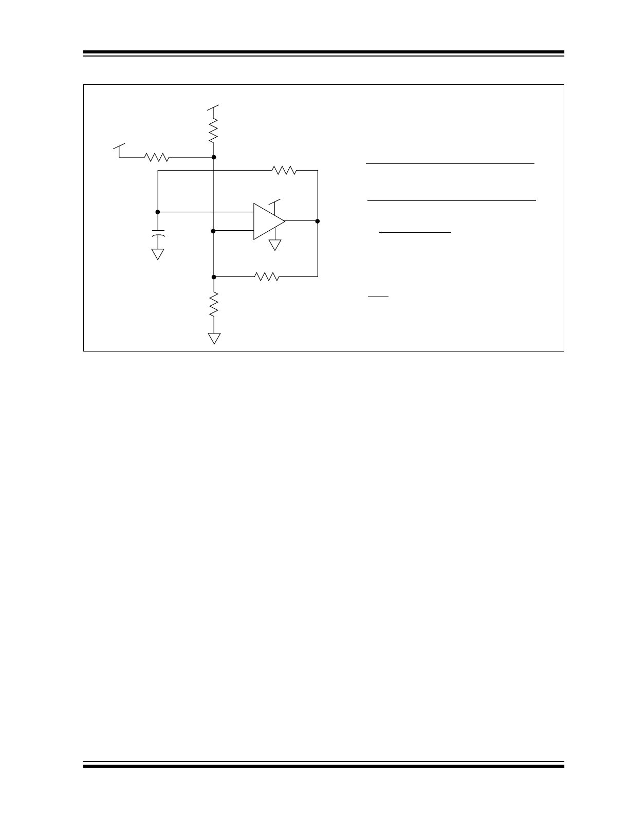
Figure 4-6 shows the circuit for a pulse width modulator
circuit. It is essentially the same as in Figure 4-5 with
the addition of an input control voltage. When the input
control voltage is equal to one-half V
DD
, operation is
basically the same as described for the free-running
oscillator. If the input control voltage is moved above or
below one-half V
DD
, the duty cycle of the output square
wave will be altered. This is because the addition of the
control voltage at the input has now altered the trip
points. The equations for these trip points are shown in
Figure 4-6 (see V
H
and V
L
).
Pulse width sensitivity to the input voltage variations
can be increased by reducing the value of R6 from
10K
Ω
and conversely, sensitivity will be reduced by
increasing the value of R6. The values of R1 and C1
can be varied to produce the desired center frequency.
FIGURE 4-1:
COMPARATOR
EXTERNAL HYSTERESIS
CONFIGURATION
FIGURE 4-2:
PRECISION BATTERY MONITOR
V
L
V
DD
3
-----------
=
1
FREQ
-----------------
2 0.694
(
)
R4
(
)
C1
(
)
=
+
–
V
R
V
DD
V
OUT
V
SRC
R
A
R
B
R
C
TC1037
V
DD
V
DD
V
DD
R2, 330k, 1%
TC1034
R4, 470k, 1%
R5, 7.5M
R6, 7.5M
R3, 470k, 1%
R1, 270k, 1%
V
R
To System DC/DC
Converter
3V
Alkaline
TC1039
BATTFAIL
BATTLOW
CMPTR1
+
–
CMPTR2
+
–
AMP1
+
–
+
TC1037
TC1039
TC1037/TC1038/TC1039
DS21344B-page 8
2002 Microchip Technology Inc.
FIGURE 4-3:
32.768 kHz “TIME OF DAY” CLOCK OSCILLATOR
FIGURE 4-4:
NON-RETRIGGERABLE MULTIVIBRATOR
FIGURE 4-5:
SQUARE WAVE GENERATOR
+
V
DD
V
OUT
V
DD
RB
150k
RA
150k
R
C
1M
CA
100pF
32.768kHz
T
per
= 30.52
µsec
TC1037
–
+
–
+
–
V
DD
CMPTR1
CMPTR2
IN
IN
OUT
OUT
R3
1M
R4
1M
R6
562k
R7
1M
R2
100k
R1
100k
R8
D2
D1
10M
R9
243k
R5
10M
C1
100pF
R10
61.9k
A
B
C
GND
t
0
C
GND
V
DD
GND
V
DD
TC1025
TC1037
+
–
R1
100k
V
DD
R4
V
DD
R3
100k
R2
100k
C1
V
H
=
R2 (V
DD
)
R2 + (R1||R3)
V
L
=
(V
DD
) (R2||R3)
R1 + (R2||R3)
FREQ =
1
2(0.694)(R4)(C1)
TC1037
2002 Microchip Technology Inc.
DS21344B-page 9
TC1037/TC1038/TC1039
FIGURE 4-6:
PULSE WIDTH MODULATOR
+
–
R6
10k
R4
V
C
V
DD
V
DD
R1
100k
R3
100k
R2
100k
C1
FREQ =
1
2
2 (0.694) (R4) (C1)
For Square Wave Generation
Select R1 = R2 = R3
TC1037
V
H
=
V
C
=
V
DD
V
DD
(R1R2R6 + R2R3R6) + V
C
(R1R2R3)
R1R2R6 + R1R3R6 + R2R3R6 + R1R2R3
V
DD
(R2R3R6) + V
C
(R1R2R3)
R1R2R6 + R1R3R6 + R2R3R6 + R1R2R3
V
L
=
1/4
TC1037/TC1038/TC1039
DS21344B-page 10
2002 Microchip Technology Inc.
5.0
TYPICAL CHARACTERISTICS
Note:
The graphs and tables provided following this note are a statistical summary based on a limited number of
samples and are provided for informational purposes only. The performance characteristics listed herein
are not tested or guaranteed. In some graphs or tables, the data presented may be outside the specified
operating range (e.g., outside specified power supply range) and therefore outside the warranted range.
7
6
5
4
3
2
1.5
2
2.5
3
3.5
4
4.5
5
5.5
SUPPLY VOLTAGE (V)
SUPPLY VOLTAGE (V)
Comparator Propagation Delay
vs. Supply Voltage
DELAY TO RISING EDGE (
µ
sec)
Overdrive = 10mV
Overdrive = 50mV
7
6
5
4
3
2
1.5
2
2.5
3
3.5
4
4.5
5
5.5
DELAY TO FALLING EDGE (
µ
sec)
7
6
5
4
3
-40
°C
85
°C
25
°C
TEMPERATURE (
°C)
DELAY TO RISING EDGE (
µ
sec)
Overdrive = 100mV
Overdrive = 10mV
Overdrive = 50mV
Comparator Propagation Delay
vs. Supply Voltage
Comparator Propagation Delay
vs. Temperature
T
A
= 25°C
C
L
= 100pF
T
A
= 25°C
C
L
= 100pF
Overdrive = 100mV
V
DD
= 4V
V
DD
= 5V
V
DD
= 2V
V
DD
= 3V
-40
°C
85
°C
25
°C
2.5
2.0
1.5
1.0
.5
0
0
1
2
3
4
5
6
V
DD
- V
OUT
(V)
I
SOURCE
(mA)
7
6
5
4
3
Comparator Output Swing
vs. Output Source Current
DELAY TO FALLING EDGE (
µ
sec)
Overdrive = 100mV
2.5
2.0
1.5
1.0
.5
0
0
1
2
3
4
5
Comparator Propagation Delay
vs. Temperature
Comparator Output Swing
vs. Output Sink Current
TEMPERATURE (
°C)
I
SINK
(mA)
V
DD
= 4V
V
DD
= 5V
V
DD
= 2V
V
DD
= 3V
T
A
= 25°C
T
A
= 25°C
V
DD
= 3V
V
DD
= 1.8V
V
DD
= 5.5V
V
DD
= 3V
V
DD
= 1.8V
V
DD
= 5.5V
V
OUT
- V
SS
(V)
6
60
50
Sinking
40
30
20
10
0
0
1
2
3
4
5
6
OUTPUT SHORT-CIRCUIT CURRENT (mA)
SUPPLY VOLTAGE (V)
Comparator Output Short-Circuit
Current vs. Supply Voltage
Sourcing
T
A
= -40
°C
T
A
= -40
°C
T
A
= 25
°C
T
A
= 85
°C
T
A
= 25
°C
T
A
= 85
°C
REFERENCE VOLTAGE (V)
1.240
1.220
1.200
1.180
1.160
1.140
0
2
4
6
8
10
LOAD CURRENT (mA)
Reference Voltage vs.
Load Current
V
DD
= 1.8V
V
DD
= 3V
V
DD
= 5.5V
Sinking
Sourcing
V
DD
= 1.8V
V
DD
= 3V
V
DD
= 5.5V
4
3
2
1
0
0
100
200
300
400
SUPPLY AND REFERENCE VOLTAGES (V)
TIME (
µsec)
Line Transient
Response of V
REF
V
DD
V
REF
2002 Microchip Technology Inc.
DS21344B-page 1
Features
• Tiny SOT-23A Packages
• Optimized for Single Supply Operation
• Ultra Low Input Bias Current: Less than 100pA
• Low Quiescent Current: 4
µ
A (TC1037),
Shutdown Mode: 4
µ
A, 0.05
µ
A (TC1038),
6
µ
A (TC1039)
• Shutdown Mode (TC1038)
• 2.0% Accurate Independent Voltage Reference
(TC1039)
• Rail-to-Rail Inputs and Outputs
• Operation Down to V
DD
= 1.8V
Applications
• Power Management Circuits
• Battery Operated Equipment
• Consumer Products
Device Selection Table
Package Types
General Description
The TC1037/TC1038/TC1039 are single, low-power
comparators designed for low-power applications.
These comparators are specifically designed for
operation from a single supply. However, operation
from dual supplies also is possible, and power supply
current is independent of the magnitude of the power
supply voltage. The TC1037/TC1038/TC1039 operate
from two 1.5V alkaline cells down to V
DD
= 1.8V. Active
supply current is 4
µ
A for the TC1037/TC1038 and 6
µ
A
for the TC1039. Input and output swing of these
devices is rail-to-rail.
An active low shutdown input, SHDN, is available on
the TC1038 and disables the comparator, placing its
output in a high-impedance state. The TC1038 draws
only 0.05
µ
A (typical) when the shutdown mode is
active.
An internally biased 1.20V bandgap reference is
included in the TC1039. The reference is accurate to
2.0 percent tolerance. This reference is independent of
the comparator in the TC1039.
Packaged in a 5-Pin SOT-23A (TC1037) or 6-Pin
SOT-23A (TC1038/TC1039), these single comparators
are ideal for applications requiring high integration,
small size and low power.
Functional Block Diagram
Part Number
Package
Temperature
Range
TC1037CECT
5-Pin SOT-23A
-40°C to +85°C
TC1038CECH
6-Pin SOT-23A
-40°C to +85°C
TC1039CECH
6-Pin SOT-23A
-40°C to +85°C
OUTPUT
V
SS
IN+
V
DD
IN-
5-Pin SOT-23A
TC1037ECT
1
3
5
4
2
OUTPUT
V
SS
IN+
V
DD
IN-
SHDN
6-Pin SOT-23A
TC1038ECH
1
3
6
4
5
2
OUTPUT
V
SS
IN+
V
DD
IN-
REF
6-Pin SOT-23A
TC1039ECH
1
3
6
4
5
2
NOTE: 5-Pin SOT-23A is equivalent to the EIAJ SC-74A.
6-Pin SOT-23A is equivalent to the EIAJ SC-74.
+
–
OUTPUT
IN+
TC1037
+
–
OUTPUT
IN+
TC1038
1
2
3
5
4
6
5
4
1
2
3
6
5
4
2
3
V
SS
V
DD
IN-
V
DD
SHDN
IN-
V
SS
1
+
–
OUTPUT
IN+
TC1039
V
SS
Voltage
Reference
V
DD
IN-
REF
TC1037/TC1038/TC1039
Linear Building Block – Single Comparator in SOT Packages
TC1037/TC1038/TC1039
DS21344B-page 2
2002 Microchip Technology Inc.
1.0
ELECTRICAL
CHARACTERISTICS
ABSOLUTE MAXIMUM RATINGS*
Supply Voltage ......................................................6.0V
Voltage on Any Pin .......... (V
SS
– 0.3V) to (V
DD
+ 0.3V)
Junction Temperature....................................... +150°C
Operating Temperature Range............. -40°C to +85°C
Storage Temperature Range .............. -55°C to +150°C
*Stresses above those listed under "Absolute Maximum
Ratings" may cause permanent damage to the device. These
are stress ratings only and functional operation of the device
at these or any other conditions above those indicated in the
operation sections of the specifications is not implied.
Exposure to Absolute Maximum Rating conditions for
extended periods may affect device reliability.
TC1037/TC1038/TC1039 ELECTRICAL SPECIFICATIONS
Electrical Characteristics: Typical values apply at 25°C and V
DD
= 3.0V. Minimum and maximum values apply for T
A
= -40° to
+85°C and V
DD
= 1.8V to 5.5V, unless otherwise specified.
Symbol
Parameter
Min
Typ
Max
Units
Test Conditions
V
DD
Supply Voltage
1.8
—
5.5
V
I
Q
Supply Current, Operating (TC1039)
(TC1037/TC1038)
—
—
6
4
10
8
µ
A
µ
A
All Outputs Unloaded,
SHDN = V
DD
for TC1038
I
SHDN
Supply Current Shutdown Mode
(TC1038 Only)
—
—
0.3
µ
A
SHDN = V
SS
Shutdown Input (TC1038 Only)
V
IH
Input High Threshold
80% V
DD
—
—
V
V
IL
Input Low Threshold
—
—
20% V
DD
V
I
SI
Shutdown Input Current
—
—
±100
nA
Comparator
R
OUT
(SD)
Output Resistance in Shutdown
20
—
—
M
Ω
SHDN = V
SS
(TC1038 Only)
C
OUT
(SD)
Output Capacitance in Shutdown
—
—
5
pF
SHDN = V
SS
(TC1038 Only)
T
SEL
Select Time
—
20
—
µ
sec
V
OUT
Valid from SHDN = V
IH
R
L
= 10k
Ω
to V
SS
(TC1038 Only)
T
DESEL
Deselect Time
—
500
—
nsec
V
OUT
Valid from SHDN = V
IL
R
L
= 10k
Ω
to V
SS
V
ICMR
Common Mode Input Voltage Range V
SS
– 0.2
—
V
DD
+ 0.2
V
A
VOL
Large Signal Voltage Gain
—
100
—
V/mV
R
L
= 10k
Ω
, V
DD
= 5V
GBWP
Gain Bandwidth Product
—
90
—
kHz
V
DD
= 1.8V to 5.5V;
V
O
= V
DD
to V
SS
V
OS
Input Offset Voltage
–5
–5
—
+5
+5
mV
mV
V
DD
= 3V, V
CM
= 1.5V, T
A
= 25°C,
T
A
= -40°C to 85°C
I
B
Input Bias Current
—
—
±100
pA
T
A
= 25°C;
IN+, IN- = V
DD
to V
SS
V
OH
Output High Voltage
V
DD
– 0.3
—
—
V
R
L
= 10k
Ω
to V
SS
V
OL
Output Low Voltage
—
—
0.3
V
R
L
= 10k
Ω
to V
DD
CMRR
Common Mode Rejection Ratio
66
—
—
dB
T
A
= 25°C; V
DD
= 5V;
V
CM
= V
DD
to V
SS
PSRR
Power Supply Rejection Ratio
60
—
—
dB
T
A
= 25°C; V
CM
= 1.2V;
V
DD
= 1.8V to 5V
I
SRC
Output Source Current
1
—
—
mA
IN+ = V
DD
, IN- = V
SS
Output Shorted to V
SS
V
DD
= 1.8V
I
SINK
Output Sink Current
2
—
—
mA
IN+ = V
SS
, IN- = V
SS
Output Shorted to V
SS
V
DD
= 1.8V
T
PD1
Response Time
—
4
—
µ
sec
100mV Overdrive, C
L
= 100pF
T
PD2
Response Time
—
6
—
µ
sec
10mV Overdrive, C
L
= 100pF
2002 Microchip Technology Inc.
DS21344B-page 3
TC1037/TC1038/TC1039
TC1037/TC1038/TC1039 ELECTRICAL SPECIFICATIONS (CONTINUED)
Electrical Characteristics: Typical values apply at 25°C and V
DD
= 3.0V. Minimum and maximum values apply for T
A
= -40° to
+85°C and V
DD
= 1.8V to 5.5V, unless otherwise specified.
Symbol
Parameter
Min
Typ
Max
Units
Test Conditions
Voltage Reference (TC1039 Only)
V
REF
Reference Voltage
1.176
1.200
1.224
V
I
REF(SOURCE)
Source Current
50
—
—
µ
A
I
REF(SINK)
Sink Current
50
—
—
µ
A
C
L(REF)
Load Capacitance
—
—
100
pF
E
VREF
Noise Voltage
—
20
—
µ
V
RMS
100Hz to 100kHz
e
VREF
Noise Voltage Density
—
1.0
—
µ
V/
√
Hz 1kHz
TC1037/TC1038/TC1039
DS21344B-page 4
2002 Microchip Technology Inc.
2.0
PIN DESCRIPTIONS
The description of the pins are listed in Table 2-1.
TABLE 2-1:
PIN FUNCTION TABLE
Pin No.
TC1037
(5-Pin SOT-23A)
Symbol
Description
1
OUTPUT
Comparator output.
2
V
SS
Negative power supply.
3
IN+
Comparator non-inverting input.
4
IN-
Comparator inverting input.
5
V
DD
Positive power supply.
Pin No.
TC1038
(6-Pin SOT-23A)
Symbol
Description
1
OUTPUT
Comparator output.
2
V
SS
Negative power supply.
3
IN+
Comparator non-inverting input.
4
IN-
Comparator inverting input.
5
SHDN
Active low shutdown input (TC1038 only). A low input on this pin disables the comparator
and places the output terminal in a high impedance state.
6
V
DD
Positive power supply.
Pin No.
TC1039
(6-Pin SOT-23A)
Symbol
Description
1
OUTPUT
Comparator output.
2
V
SS
Negative power supply.
3
IN+
Comparator non-inverting input.
4
IN-
Comparator inverting input.
5
REF
1.20V bandgap voltage reference output (TC1039 only).
6
V
DD
Positive power supply.
2002 Microchip Technology Inc.
DS21344B-page 5
TC1037/TC1038/TC1039
3.0
DETAILED DESCRIPTION
The TC1037/TC1038/TC1039 are a series of very low
power, linear building block products targeted at low
voltage, single supply applications. The TC1037/
TC1038/TC1039 minimum operating voltage is 1.8V
and typical supply current is only 4
µ
A for the TC1037
and TC1038 (fully enabled) and 6
µ
A for the TC1039.
3.1
Comparator
The
TC1037/8/9
contain
one
comparator.
The
comparator’s input range extends beyond both supply
voltages by 200mV and the outputs will swing to within
several millivolts of the supplies depending on the load
current being driven.
The comparator exhibits a propagation delay and
supply current which is largely independent of supply
voltage. The low input bias current and offset voltage
makes it suitable for high impedance precision
applications.
The TC1038 comparator is disabled during shutdown
and has a high impedance output.
3.2
Voltage Reference
A 2.0% tolerance, internally biased, 1.20V bandgap
voltage reference is included in the TC1039. It has a
push-pull output capable of sourcing and sinking at
least 50
µ
A.
3.3
Shutdown Input (TC1038 Only)
SHDN at V
IL
disables the comparator and reduces the
supply current to less than 0.3
µ
A. The SHDN input
cannot be allowed to float. When not used, connect it to
V
DD
. The comparator’s output is in a high impedance
state when the TC1038 is disabled. The comparator’s
inputs can be driven from rail-to-rail by an external
voltage when the TC1038 is disabled. No latchup will
occur when the device is driven to its enabled state
when SHDN is set to V
IH
.
4.0
TYPICAL APPLICATIONS
The TC1037/TC1038/TC1039 family lends itself to a
wide variety of applications, particularly in battery
powered systems. It typically finds application in power
management, processor supervisory and interface
circuitry.
4.1
External Hysteresis (Comparator)
Hysteresis can be set externally with two resistors
using positive feedback techniques (see Figure 4-1).
The design procedure for setting external comparator
hysteresis is as follows:
1.
Choose the feedback resistor R
C
. Since the
input bias current of the comparator is at most
100pA, the current through R
C
can be set to
100nA (i.e., 1000 times the input bias current)
and retain excellent accuracy. The current
through R
C
at the comparator’s trip point is V
R
/
R
C
where V
R
is a stable reference voltage.
2.
Determine the hysteresis voltage (V
HY
) between
the upper and lower thresholds.
3.
Calculate R
A
as follows:
EQUATION 4-1:
4.
Choose the rising threshold voltage for V
SRC
(V
THR
).
5.
Calculate R
B
as follows:
EQUATION 4-2:
6.
Verify
the
threshold
voltages
with
these
formulas:
V
SRC
rising:
EQUATION 4-3:
V
SRC
falling:
EQUATION 4-4:
R
A
R
C
V
HY
V
DD
-----------
=
R
B
1
V
THR
V
R
R
A
×
---------------------
1
R
A
-------
–
1
R
C
-------
–
-----------------------------------------------------------
=
V
TH R
V
R
(
)
R
A
(
)
1
R
A
-------
1
R
B
-------
1
R
C
-------
+
+
=
V
THF
V
THR
R
A
V
DD
×
R
C
-------------------------
–
=
TC1037/TC1038/TC1039
DS21344B-page 6
2002 Microchip Technology Inc.
4.2
Precision Battery Monitor
Figure 4-2 is a precision battery low/battery dead
monitoring circuit. Typically, the battery low output
warns the user that a battery dead condition is
imminent. Battery dead typically initiates a forced
shutdown to prevent operation at low internal supply
voltages (which can cause unstable system operation).
The circuit in Figure 4-2 uses a TC1034, a TC1037 and
a TC1039, and only six external resistors. AMP 1 is a
simple buffer, while CMPTR1 and CMPTR2 provide
precision voltage detection using V
R
as a reference.
Resistors R2 and R4 set the detection threshold for
BATT LOW, while resistors R1 and R3 set the detection
threshold for BATT FAIL. The component values shown
assert BATT LOW at 2.2V (typical) and BATT FAIL at
2.0V (typical). Total current consumed by this circuit is
typically 16
µ
A at 3V. Resistors R5 and R6 provide
hysteresis for comparators CMPTR1 and CMPTR2,
respectively.
4.3
32.768 kHz “Time Of Day Clock”
Crystal Controlled Oscillator
A very stable oscillator driver can be designed by using
a crystal resonator as the feedback element. Figure 4-3
shows a typical application circuit using this technique
to develop a clock driver for a Time Of Day (TOD) clock
chip. The value of R
A
and R
B
determine the DC voltage
level at which the comparator trips – in this case one-
half of V
DD
. The RC time constant of R
C
and C
A
should
be set several times greater than the crystal oscillator’s
period, which will ensure a 50% duty cycle by maintain-
ing a DC voltage at the inverting comparator input
equal to the absolute average of the output signal.
4.4
Non-Retriggerable One Shot
Multivibrator
Using two comparators, a non-retriggerable one shot
multivibrator can be designed using the circuit configu-
ration of Figure 4-4. A key feature of this design is that
the pulse width is independent of the magnitude of the
supply voltage because the charging voltage and the
intercept voltage are a fixed percentage of V
DD
. In
addition, this one shot is capable of pulse width with as
much as a 99% duty cycle and exhibits input lockout to
ensure that the circuit will not re-trigger before the
output pulse has completely timed out. The trigger level
is the voltage required at the input to raise the voltage
at node A higher than the voltage at node B, and is set
by the resistive divider R4 and R10 and the impedance
network composed of R1, R2 and R3. When the one
shot has been triggered, the output of CMPTR2 is high,
causing the reference voltage at the non-inverting input
of CMPTR1 to go to V
DD
. This prevents any additional
input pulses from disturbing the circuit until the output
pulse has timed out.
The value of the timing capacitor C1 must be small
enough to allow CMPTR1 to discharge C1 to a diode
voltage before the feedback signal from CMPTR2
(through R10) switches CMPTR1 to its high state and
allows C1 to start an exponential charge through R5.
Proper circuit action depends upon rapidly discharging
C1 through the voltage set by R6, R9 and D2 to a final
voltage of a small diode drop. Two propagation delays
after the voltage on C1 drops below the level on the
non-inverting input of CMPTR2, the output of CMPTR1
switches to the positive rail and begins to charge C1
through R5. The time delay which sets the output pulse
width results from C1 charging to the reference voltage
set by R6, R9 and D2, plus four comparator propaga-
tion delays. When the voltage across C1 charges
beyond the reference, the output pulse returns to
ground and the input is again ready to accept a trigger
signal.
4.5
Oscillators and Pulse Width
Modulators
Microchip’s linear building block comparators adapt
well to oscillator applications for low frequencies (less
than 100kHz). Figure 4-5 shows a symmetrical square
wave generator using a minimum number of compo-
nents. The output is set by the RC time constant of R4
and C1, and the total hysteresis of the loop is set by R1,
R2 and R3. The maximum frequency of the oscillator is
limited only by the large signal propagation delay of the
comparator in addition to any capacitive loading at the
output which degrades the slew rate.
To analyze this circuit, assume that the output is initially
high. For this to occur, the voltage at the inverting input
must be less than the voltage at the non-inverting input.
Therefore, capacitor C1 is discharged. The voltage at
the non-inverting input (V
H
) is:
EQUATION 4-5:
where, if R1 = R2 = R3, then:
EQUATION 4-6:
V
H
R2 V
DD
(
)
R2
R1
R3
||
(
)
+
[
]
---------------------------------------------
=
V
H
2 V
DD
(
)
3
-------------------
=
2002 Microchip Technology Inc.
DS21344B-page 7
TC1037/TC1038/TC1039
Capacitor C1 will charge up through R4. When the
voltage of the comparator's inverting input is equal to
V
H
, the comparator output will switch. With the output
at ground potential, the value at the non-inverting input
terminal (V
L
) is reduced by the hysteresis network to a
value given by:
EQUATION 4-7:
Using the same resistors as before, capacitor C1 must
now discharge through R4 toward ground. The output
will return to a high state when the voltage across the
capacitor has discharged to a value equal to V
L
. The
period of oscillation will be twice the time it takes for the
RC circuit to charge up to one half its final value. The
period can be calculated from:
EQUATION 4-8:
The frequency stability of this circuit should only be a
function of the external component tolerances.
Figure 4-6 shows the circuit for a pulse width modulator
circuit. It is essentially the same as in Figure 4-5 with
the addition of an input control voltage. When the input
control voltage is equal to one-half V
DD
, operation is
basically the same as described for the free-running
oscillator. If the input control voltage is moved above or
below one-half V
DD
, the duty cycle of the output square
wave will be altered. This is because the addition of the
control voltage at the input has now altered the trip
points. The equations for these trip points are shown in
Figure 4-6 (see V
H
and V
L
).
Pulse width sensitivity to the input voltage variations
can be increased by reducing the value of R6 from
10K
Ω
and conversely, sensitivity will be reduced by
increasing the value of R6. The values of R1 and C1
can be varied to produce the desired center frequency.
FIGURE 4-1:
COMPARATOR
EXTERNAL HYSTERESIS
CONFIGURATION
FIGURE 4-2:
PRECISION BATTERY MONITOR
V
L
V
DD
3
-----------
=
1
FREQ
-----------------
2 0.694
(
)
R4
(
)
C1
(
)
=
+
–
V
R
V
DD
V
OUT
V
SRC
R
A
R
B
R
C
TC1037
V
DD
V
DD
V
DD
R2, 330k, 1%
TC1034
R4, 470k, 1%
R5, 7.5M
R6, 7.5M
R3, 470k, 1%
R1, 270k, 1%
V
R
To System DC/DC
Converter
3V
Alkaline
TC1039
BATTFAIL
BATTLOW
CMPTR1
+
–
CMPTR2
+
–
AMP1
+
–
+
TC1037
TC1039
TC1037/TC1038/TC1039
DS21344B-page 8
2002 Microchip Technology Inc.
FIGURE 4-3:
32.768 kHz “TIME OF DAY” CLOCK OSCILLATOR
FIGURE 4-4:
NON-RETRIGGERABLE MULTIVIBRATOR
FIGURE 4-5:
SQUARE WAVE GENERATOR
+
V
DD
V
OUT
V
DD
RB
150k
RA
150k
R
C
1M
CA
100pF
32.768kHz
T
per
= 30.52
µsec
TC1037
–
+
–
+
–
V
DD
CMPTR1
CMPTR2
IN
IN
OUT
OUT
R3
1M
R4
1M
R6
562k
R7
1M
R2
100k
R1
100k
R8
D2
D1
10M
R9
243k
R5
10M
C1
100pF
R10
61.9k
A
B
C
GND
t
0
C
GND
V
DD
GND
V
DD
TC1025
TC1037
+
–
R1
100k
V
DD
R4
V
DD
R3
100k
R2
100k
C1
V
H
=
R2 (V
DD
)
R2 + (R1||R3)
V
L
=
(V
DD
) (R2||R3)
R1 + (R2||R3)
FREQ =
1
2(0.694)(R4)(C1)
TC1037
2002 Microchip Technology Inc.
DS21344B-page 9
TC1037/TC1038/TC1039
FIGURE 4-6:
PULSE WIDTH MODULATOR
+
–
R6
10k
R4
V
C
V
DD
V
DD
R1
100k
R3
100k
R2
100k
C1
FREQ =
1
2
2 (0.694) (R4) (C1)
For Square Wave Generation
Select R1 = R2 = R3
TC1037
V
H
=
V
C
=
V
DD
V
DD
(R1R2R6 + R2R3R6) + V
C
(R1R2R3)
R1R2R6 + R1R3R6 + R2R3R6 + R1R2R3
V
DD
(R2R3R6) + V
C
(R1R2R3)
R1R2R6 + R1R3R6 + R2R3R6 + R1R2R3
V
L
=
1/4
TC1037/TC1038/TC1039
DS21344B-page 10
2002 Microchip Technology Inc.
5.0
TYPICAL CHARACTERISTICS
Note:
The graphs and tables provided following this note are a statistical summary based on a limited number of
samples and are provided for informational purposes only. The performance characteristics listed herein
are not tested or guaranteed. In some graphs or tables, the data presented may be outside the specified
operating range (e.g., outside specified power supply range) and therefore outside the warranted range.
7
6
5
4
3
2
1.5
2
2.5
3
3.5
4
4.5
5
5.5
SUPPLY VOLTAGE (V)
SUPPLY VOLTAGE (V)
Comparator Propagation Delay
vs. Supply Voltage
DELAY TO RISING EDGE (
µ
sec)
Overdrive = 10mV
Overdrive = 50mV
7
6
5
4
3
2
1.5
2
2.5
3
3.5
4
4.5
5
5.5
DELAY TO FALLING EDGE (
µ
sec)
7
6
5
4
3
-40
°C
85
°C
25
°C
TEMPERATURE (
°C)
DELAY TO RISING EDGE (
µ
sec)
Overdrive = 100mV
Overdrive = 10mV
Overdrive = 50mV
Comparator Propagation Delay
vs. Supply Voltage
Comparator Propagation Delay
vs. Temperature
T
A
= 25°C
C
L
= 100pF
T
A
= 25°C
C
L
= 100pF
Overdrive = 100mV
V
DD
= 4V
V
DD
= 5V
V
DD
= 2V
V
DD
= 3V
-40
°C
85
°C
25
°C
2.5
2.0
1.5
1.0
.5
0
0
1
2
3
4
5
6
V
DD
- V
OUT
(V)
I
SOURCE
(mA)
7
6
5
4
3
Comparator Output Swing
vs. Output Source Current
DELAY TO FALLING EDGE (
µ
sec)
Overdrive = 100mV
2.5
2.0
1.5
1.0
.5
0
0
1
2
3
4
5
Comparator Propagation Delay
vs. Temperature
Comparator Output Swing
vs. Output Sink Current
TEMPERATURE (
°C)
I
SINK
(mA)
V
DD
= 4V
V
DD
= 5V
V
DD
= 2V
V
DD
= 3V
T
A
= 25°C
T
A
= 25°C
V
DD
= 3V
V
DD
= 1.8V
V
DD
= 5.5V
V
DD
= 3V
V
DD
= 1.8V
V
DD
= 5.5V
V
OUT
- V
SS
(V)
6
60
50
Sinking
40
30
20
10
0
0
1
2
3
4
5
6
OUTPUT SHORT-CIRCUIT CURRENT (mA)
SUPPLY VOLTAGE (V)
Comparator Output Short-Circuit
Current vs. Supply Voltage
Sourcing
T
A
= -40
°C
T
A
= -40
°C
T
A
= 25
°C
T
A
= 85
°C
T
A
= 25
°C
T
A
= 85
°C
REFERENCE VOLTAGE (V)
1.240
1.220
1.200
1.180
1.160
1.140
0
2
4
6
8
10
LOAD CURRENT (mA)
Reference Voltage vs.
Load Current
V
DD
= 1.8V
V
DD
= 3V
V
DD
= 5.5V
Sinking
Sourcing
V
DD
= 1.8V
V
DD
= 3V
V
DD
= 5.5V
4
3
2
1
0
0
100
200
300
400
SUPPLY AND REFERENCE VOLTAGES (V)
TIME (
µsec)
Line Transient
Response of V
REF
V
DD
V
REF