
2002 Microchip Technology Inc.
DS21341B-page 1
Features
• Optimized for Single Supply Operation
• Small Package: 16-Pin QSOP
• Ultra Low Input Bias Current: Less than 100pA
• Low Quiescent Current, Operating: 20
µ
A (Typ.),
Shutdown Mode: 6
µ
A (Typ.)
• Rail-to-Rail Inputs and Outputs
• Operates Down to 1.8V
• Can Shut Down One, Two or Three Op Amps
Applications
• Power Management Circuits
• Battery Operated Equipment
• Consumer Products
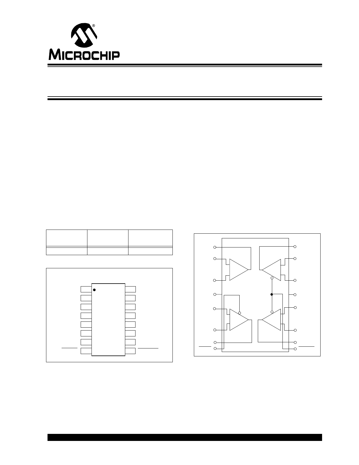
Device Selection Table
Package Type
General Description
The TC1030 is a quad CMOS operational amplifier
designed for low power applications. It has a typical
operating supply current of 20
µ
A which is constant over
the supply voltage range of 1.8V to 5.5V.
Each op amp has rail-to-rail inputs and output which
allow operation at low supply voltages with large input
and output signal swings. Two active low shutdown
pins are provided. One pin disables op amp B while the
other disables op amps C and D. Op amp A is always
active. When disabled, the outputs of op amps B, C and
D are in a high impedance state.
Packaged in a 16-Pin QSOP, the TC1030 is ideal for
battery operated applications.
The TC1030 is packaged in a 16-Pin QSOP, making it
ideal for battery operated applications.
Functional Block Diagram
Part Number
Package
Temperature
Range
TC1030EQR
16-Pin QSOP
-40°C to +85°C
TC1030EQR
1
2
3
4
16
15
14
SHDNB
SHDNC/D
5
6
7
8
13
12
11
10
9
16-Pin QSOP
OUTA
INA-
INA+
V
DD
OUTD
IND-
IND+
V
SS
INC+
INC-
OUTC
INB+
INB-
OUTB
OUTA
INA-
INA+
IND-
IND+
V
DD
V
SS
INC+
INC-
OUTC
INB+
INB-
OUTB
SHDNB
OUTD
+
–
+
–
+
–
+
–
A
B
C
D
SHDNC/D
1
2
3
4
5
6
7
8
16
15
14
13
12
11
10
9
TC1030
TC1030
Linear Building Block – Quad Low Power Op Amp
with Shutdown Modes
TC1030
DS21341B-page 2
2002 Microchip Technology Inc.
1.0
ELECTRICAL
CHARACTERISTICS
ABSOLUTE MAXIMUM RATINGS*
Supply Voltage ......................................................6.0V
Voltage on Any Pin .......... (V
SS
– 0.3V) to (V
DD
+ 0.3V)
Junction Temperature....................................... +150°C
Operating Temperature Range............. -40°C to +85°C
Storage Temperature Range .............. -55°C to +150°C
*Stresses above those listed under "Absolute Maximum
Ratings" may cause permanent damage to the device. These
are stress ratings only and functional operation of the device
at these or any other conditions above those indicated in the
operation sections of the specifications is not implied.
Exposure to Absolute Maximum Rating conditions for
extended periods may affect device reliability.
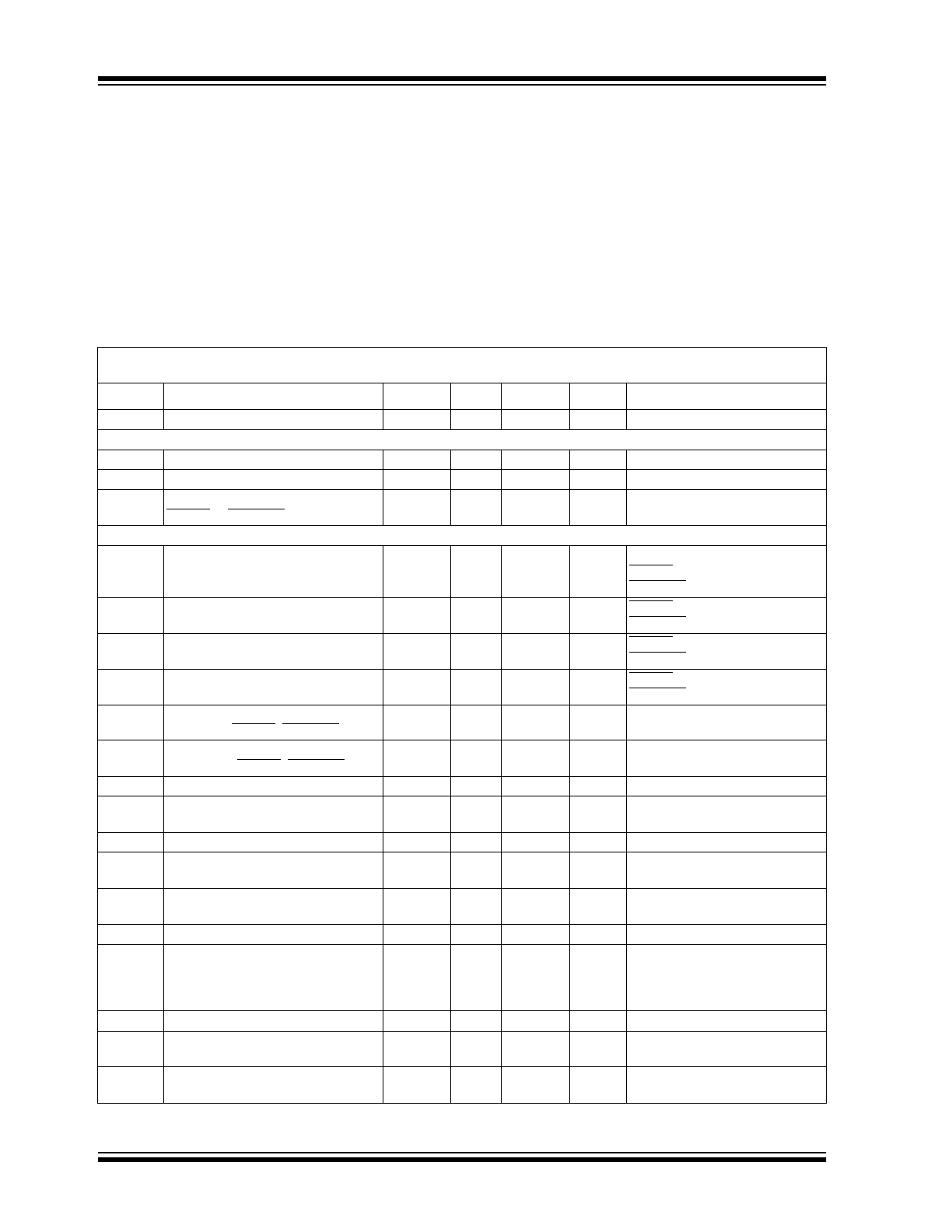
TC1030 ELECTRICAL SPECIFICATIONS
Electrical Characteristics: Typical values apply at 25°C and V
DD
= 3.0V; T
A
= -40° to +85°C, and V
DD
= 1.8V to 5.5V, unless
otherwise specified.
Symbol
Parameter
Min
Typ
Max
Units
Test Conditions
V
DD
Supply Voltage
1.8
—
5.5
V
Shutdown Inputs
V
IH
Input High Threshold
80% V
DD
—
—
V
V
IL
Input Low Threshold
—
—
20% V
DD
V
I
SI
Shutdown Input Current,
SHDNB or SHDNC/D
—
—
±100
nA
Op Amps
I
Q
Supply Current, Operating
—
20
32
µ
A
All Outputs Open,
SHDNB = V
DD
,
SHDNC/D = V
DD
I
SHDN
Supply Current Shutdown Mode
—
6
10
µ
A
SHDNB = V
SS
,
SHDNC/D = V
SS
R
OUT
(SD) Output Resistance in Shutdown
20
—
—
M
Ω
SHDNB = V
SS
,
SHDNC/D = V
SS
C
OUT
(SD) Out Capacitance in Shutdown
—
—
5
pF
SHDNB = V
SS
,
SHDNC/D = V
SS
T
SEL
Select Time
(V
OUT
from SHDNB, SHDNC/D) = V
IL
—
15
—
µ
sec
R
L
= 10k
Ω
to V
SS
T
DESEL
Deselect Time
(VOUT from SHDNB, SHDNC/D) = V
IL
—
20
—
nsec
R
L
= 10k
Ω
to V
SS
A
VOL
Large Signal Voltage Gain
—
100
—
V/mV
R
L
= 10k
Ω
, V
DD
= 5V
GBWP
Gain-Bandwidth Product
—
90
—
kHz
V
DD
= 1.8V to 5.5V;
V
O
= V
DD
to V
SS
V
ICMR
Common Mode Input Voltage Range
V
SS
– 0.2
—
V
DD
+ 0.2
V
V
OS
Input Offset Voltage
±100
±0.3
±500
±1.5
µ
V
mV
V
DD
= 3V, V
CM
= 1.5V, T
A
= 25°C,
T
A
= –40°C to 85°C
I
B
Input Bias Current
-100
50
100
pA
T
A
= 25°C;
V
CM
= V
DD
to V
SS
V
OS(DRIFT)
Input Offset Voltage Drift
—
±4
—
µ
V/°C
V
DD
= 3V; V
CM
= 1.5V
SR
Slew Rate
—
35
—
mV/
µ
sec C
L
= 100pF;
R
L
= 1 M
Ω
to GND,
Gain = 1
V
IN
= V
SS
to V
DD
V
OUT
Output Signal Swing
V
SS
+ 0.05
—
V
DD
– 0.05
V
R
L
= 10k
Ω
CMRR
Common Mode Rejection Ratio
70
—
—
dB
T
A
= 25°C; V
DD
= 5V;
V
CM
= V
DD
to V
SS
PSRR
Power Supply Rejection Ratio
80
—
—
dB
T
A
= 25°C; V
CM
= V
SS
;
V
DD
= 1.8V to 5V
2002 Microchip Technology Inc.
DS21341B-page 3
TC1030
TC1030 ELECTRICAL SPECIFICATIONS
Electrical Characteristics: Typical values apply at 25°C and V
DD
= 3.0V; T
A
= -40° to +85°C, and V
DD
= 1.8V to 5.5V, unless
otherwise specified.
Symbol
Parameter
Min
Typ
Max
Units
Test Conditions
I
SRC
Output Source Current
3
—
—
mA
V
IN
+ = V
DD
, V
IN
- = V
SS
Output Shorted to V
SS
V
DD
= 1.8V; Gain = 1
I
SINK
DC Output Sink Current
4
—
—
mA
V
IN
+ = V
SS
, V
IN
- = V
DD
Output Shorted to V
DD
V
DD
= 1.8V; Gain = 1
E
n
Input Noise Voltage
—
10
—
µ
Vpp
0.1Hz to 10Hz
e
n
Input Noise Voltage Density
—
125
—
nV/
√
HZ 1kHz
TC1030
DS21341B-page 4
2002 Microchip Technology Inc.
2.0
PIN DESCRIPTION
The description of the pins are listed in Table 2-1.
TABLE 2-1:
PIN FUNCTION TABLE
Pin No.
(16-Pin QSOP)
Symbol
Description
1
OUTA
Op amp output.
2
INA-
Op amp inverting input.
3
INA+
Op amp non-inverting input.
4
V
DD
Positive supply voltage.
5
INB+
Op amp non-inverting input.
6
INB-
Op amp inverting input.
7
OUTB
Op amp output.
8
SHDNB
Shutdown op amp B.
9
SHDNC/D
Shutdown op amps C and D.
10
OUTC
Op amp output.
11
INC-
Op amp inverting input.
12
INC+
Op amp non-inverting input.
13
V
SS
Negative supply voltage.
14
IND+
Op amp non-inverting input.
15
IND-
Op amp inverting input.
16
OUTD
Op amp output.
2002 Microchip Technology Inc.
DS21341B-page 5
TC1030
3.0
DETAILED DESCRIPTION
The TC1030 is one of a series of very low power, linear
building block products targeted at low voltage, single
supply applications. The TC1030 minimum operating
voltage is 1.8V, and maximum supply current is only
32
µ
A (fully enabled). It combines four op amps in a
single package.
Microchip’s op amps are internally compensated to be
unity-gain stable and have a typical gain bandwidth
product of 90kHz with typical slew rates of 35V/msec.
The amplifier's input range extends beyond both
supplies by 200mV and the outputs will swing to within
several millivolts of the supplies depending on the load
current being driven.
Two shutdown mode pins are incorporated for easy
adaptation to system power management schemes. In
this state, the shutdown pins allow the user to power on
one, two, three, or all four op amps (see Table 4-1). Pin
SHDNB can be used to disable op amp B and pin
SHDNC/D to disable op amps C and D. Op amp A is
always powered on regardless of the states of the
shutdown pins. When both shutdown pins are low, the
total quiescent current of the TC1030 is only 6
µ
A,
typical.
Input offset voltage is 500
µ
V max at 25°C with an input
bias current of less than 100pA. This makes the
TC1030 extremely suitable for precision, low power
applications.
4.0
TYPICAL APPLICATIONS
The TC1030 lends itself to a wide variety of
applications, particularly in battery-powered systems. It
typically finds application in power management,
process supervisory and interface circuitry.
4.1
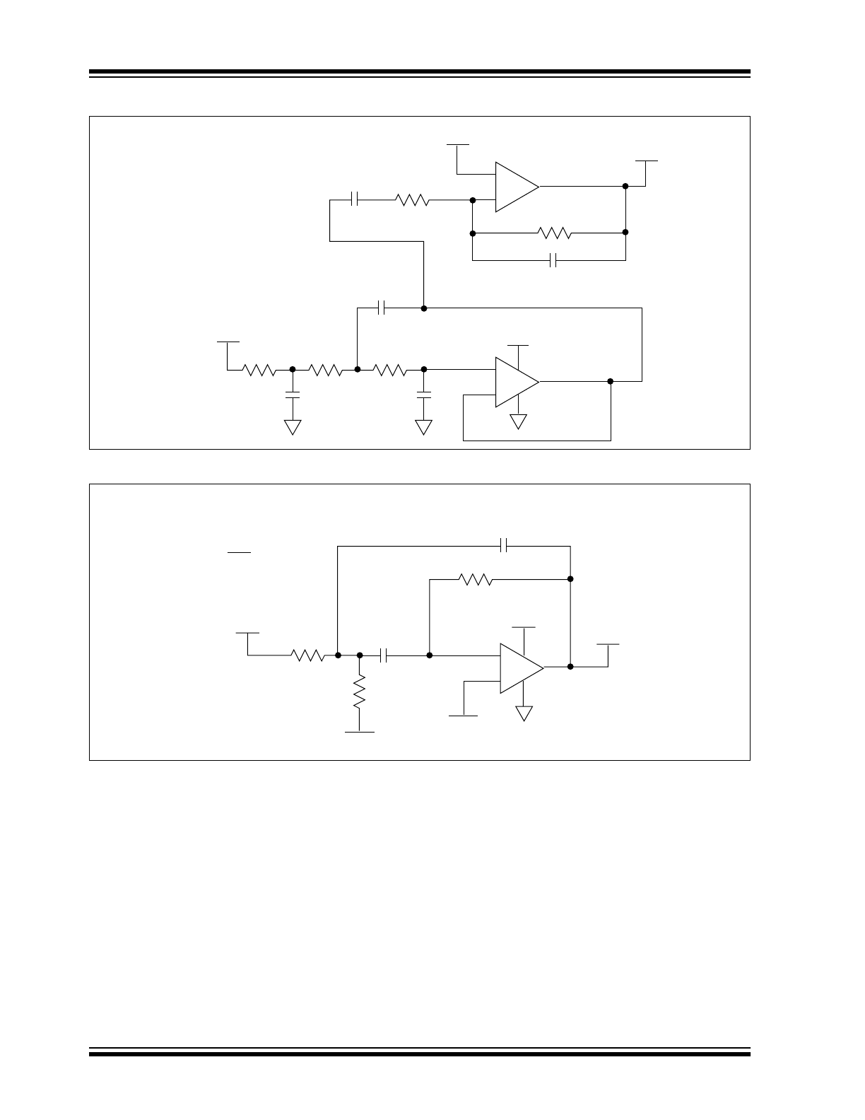
Voice Band Receive Filter
The majority of spectral energy for human voices is
found to be in a 2.7kHz frequency band from 300Hz to
3kHz. To properly recover a voice signal in applications
such as radios, cellular phones and voice pagers a low-
power bandpass filter that is matched to the human
voice spectrum can be implemented using Microchip’s
CMOS op amps. Figure 4-1 shows a unity gain multi-
pole Butterworth filter with ripple less than 0.15dB in
the human voice band. The lower 3dB cut-off frequency
is 70Hz (single order response) while the upper cut-off
frequency is 3.5kHz (fourth order response).
4.2
Supervisory Audio Tone (SAT)
Filter for Cellular
Supervisory Audio Tones (SAT) provide a reliable
transmission path between cellular subscriber units
and base stations. The SAT tone functions much like
the current/voltage used in land line telephone systems
to indicate that a phone is off the hook. The SAT tone
may be one of three frequencies: 5970, 6000 or
6030Hz. A loss of SAT implies that channel conditions
are impaired and if SAT is interrupted for more than 5
seconds a cellular call is terminated.
Figure 4-2 shows a high Q (30) second order SAT
detection bandpass filter using Microchip’s CMOS op
amp architecture. This circuit nulls all frequencies
except the three SAT tones of interest.
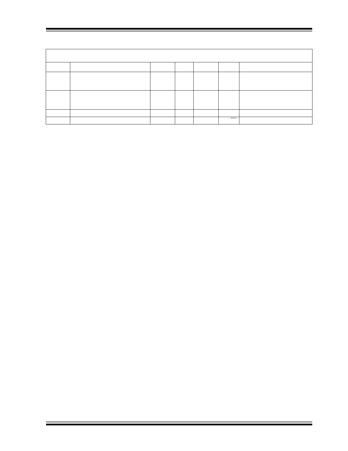
TABLE 4-1:
TC1030 SHUTDOWN POWER CONTROL LOGIC
SHDNC/D
SHDNB
OP AMPS ENABLED
OP AMPS DISABLED
MAX. DEVICE
SUPPLY CURRENT
V
IL
V
IL
A
B,C,D
10
µ
A
V
IL
V
IH
A,B
C,D
16
µ
A
V
IH
V
IL
A,C,D
B
24
µ
A
V
IH
V
IH
A,B,C,D
None
32
µ
A
TC1030
DS21341B-page 6
2002 Microchip Technology Inc.
FIGURE 4-1:
MULTI-POLE BUTTERWORTH VOICE BAND RECEIVE FILTER
FIGURE 4-2:
SECOND ORDER SAT BANDPASS FILTER
+
–
+
–
V
OUT
V
IN
21.0k
21.0k
21.0k
2400pF
470pF
750pF
V
DD
V
DD
/2
6800pF
0.1
µF
22.6k
22.6k
Gain = 0dB
Fch = 3.5kHz
-24dB/Octave
Fcl = 70Hz
+6dB/Octave
Passband Ripple
< 0.15dB
1/4
1/4
TC1030
+
–
11.2
24.3k
48.7k
.036
µF
.036
µF
V
IN
V
DD
V
OUT
Gain = 0dB
Q = F
C
BW (3dB)
Q = 30
FC = 6kHz
TC1030
1/4
V
DD
/2
V
DD
/2
2002 Microchip Technology Inc.
DS21341B-page 7
TC1030
5.0
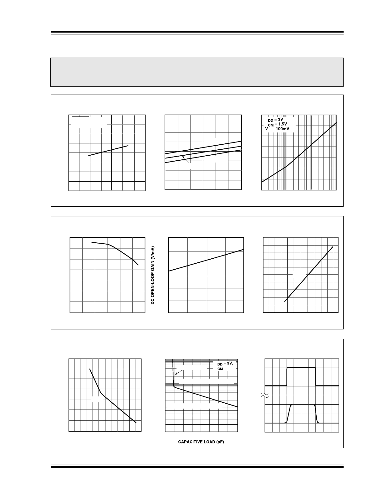
TYPICAL CHARACTERISTICS
Note:
The graphs and tables provided following this note are a statistical summary based on a limited number of
samples and are provided for informational purposes only. The performance characteristics listed herein
are not tested or guaranteed. In some graphs or tables, the data presented may be outside the specified
operating range (e.g., outside specified power supply range) and therefore outside the warranted range.
Op Amp Supply Current
vs. Temperature
Op Amp Supply Voltage
vs. Supply Current
S
UPPLY CURRENT
(µ
A
)
SUPPLY VOLTAGE (V)
S
UPPLY CURRENT
(µ
A)
TEMPERATURE (
°C)
Op Amp Power Supply Rejection
Ratio (PSRR) vs. Frequency
FREQUENCY (Hz)
P
SRR
(dB
)
28
24
26
20
22
16
12
14
18
28
24
26
20
22
16
12
14
18
0
-40
-20
0
20
40
60
80
1
2
3
4
5
6
7
1K
10K
100
0
-10
-20
-30
-40
-50
-60
-70
100K
V
V
IN =
PP
SHDNB = V
DD
SHDNC/D = V
DD
V
DD
= 5.5V
V
DD
= 1.8V
V
DD
= 3V
Op Amp Short-Circuit Current
vs. Supply Voltage
SUPPLY VOLTAGE (V)
O
UTPUT CURRENT
(mA
)
Op Amp DC Open-Loop Gain
vs. Temperature
TEMPERATURE (
°C)
3000
50
45
40
35
30
25
20
15
10
5
0
0.0
1.0
2.0
3.0
4.0
5.0
6.0
2500
2000
1500
1000
500
0
-40
°C
25
°C
85
°C
I
SINK
SUPPLY VOLTAGE (V)
DC OPEN-LOOP GAIN
(dB
)
Op Amp DC Open-Loop Gain
vs. Supply Voltage
140
120
100
80
60
40
20
0
0.0
1.0
2.0
3.0
4.0
5.0
6.0
Op Amp Load Resistance
vs. Load Capacitance
Op Amp Small-Signal
Transient Response
TIME (
µsec)
R
LO
AD
(k
Ω
)
O
UTPUT VOLTAGE
(mV
)
INPUT VOLTAGE
(mV
)
100
50
0
100
50
0
0
250 500 750 1000
10 20 30 40 50 60 70 80
90
12501500 1750 2000
100
10
1
1000
V
V
= 1.5V
10% Overshoot
Region of Marginal Stability
Region of Stable Operation
Op Amp Short-Circuit Current
vs. Supply Voltage
SUPPLY VOLTAGE (V)
O
UTPUT CURRENT
(mA
)
0
-5
-10
-15
-20
-25
-30
-35
0.0
1.0
2.0
3.0
4.0
5.0
6.0
I
SRC
TC1030
DS21341B-page 8
2002 Microchip Technology Inc.
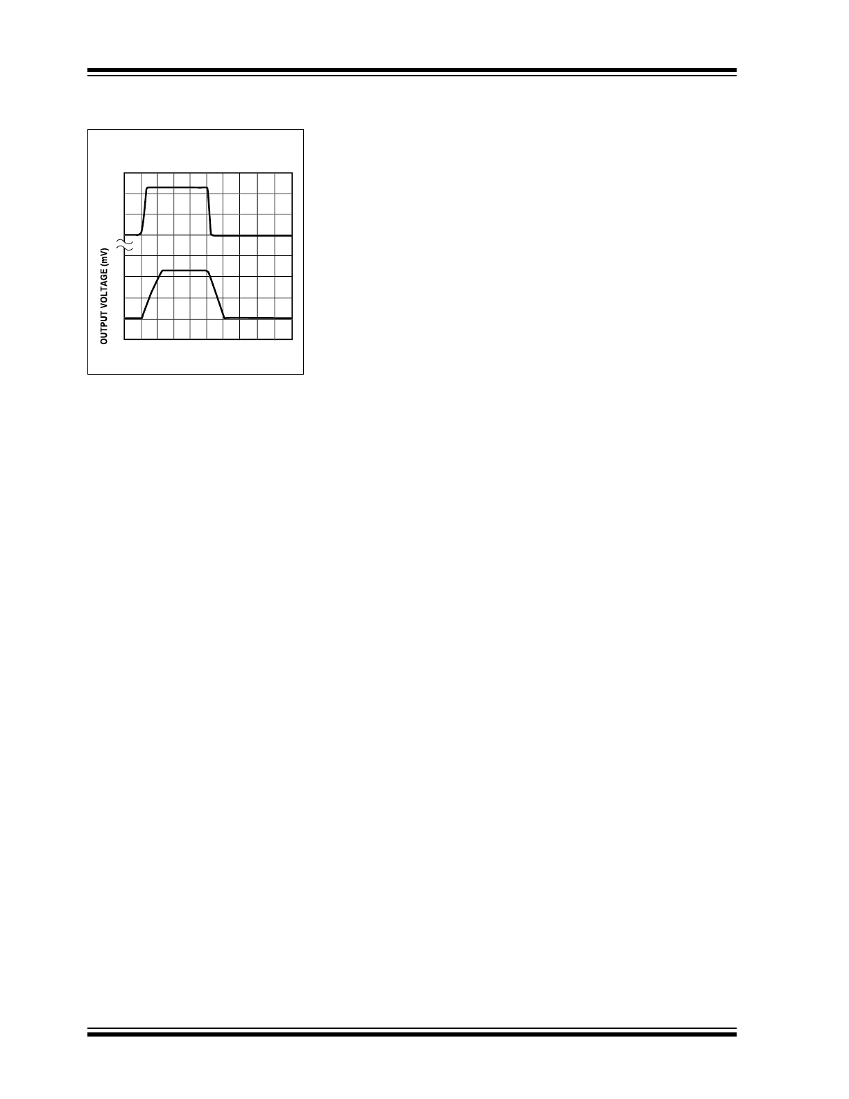
5.0
TYPICAL CHARACTERISTICS (CONTINUED)
Op Amp Large-Signal
Transient Response
TIME (
µsec)
4
6
2
0
4
6
2
0
10 20 30 40 50 60 70 80
90
INPUT VOLTAGE
(mV
)
2002 Microchip Technology Inc.
DS21341B-page 9
TC1030
6.0
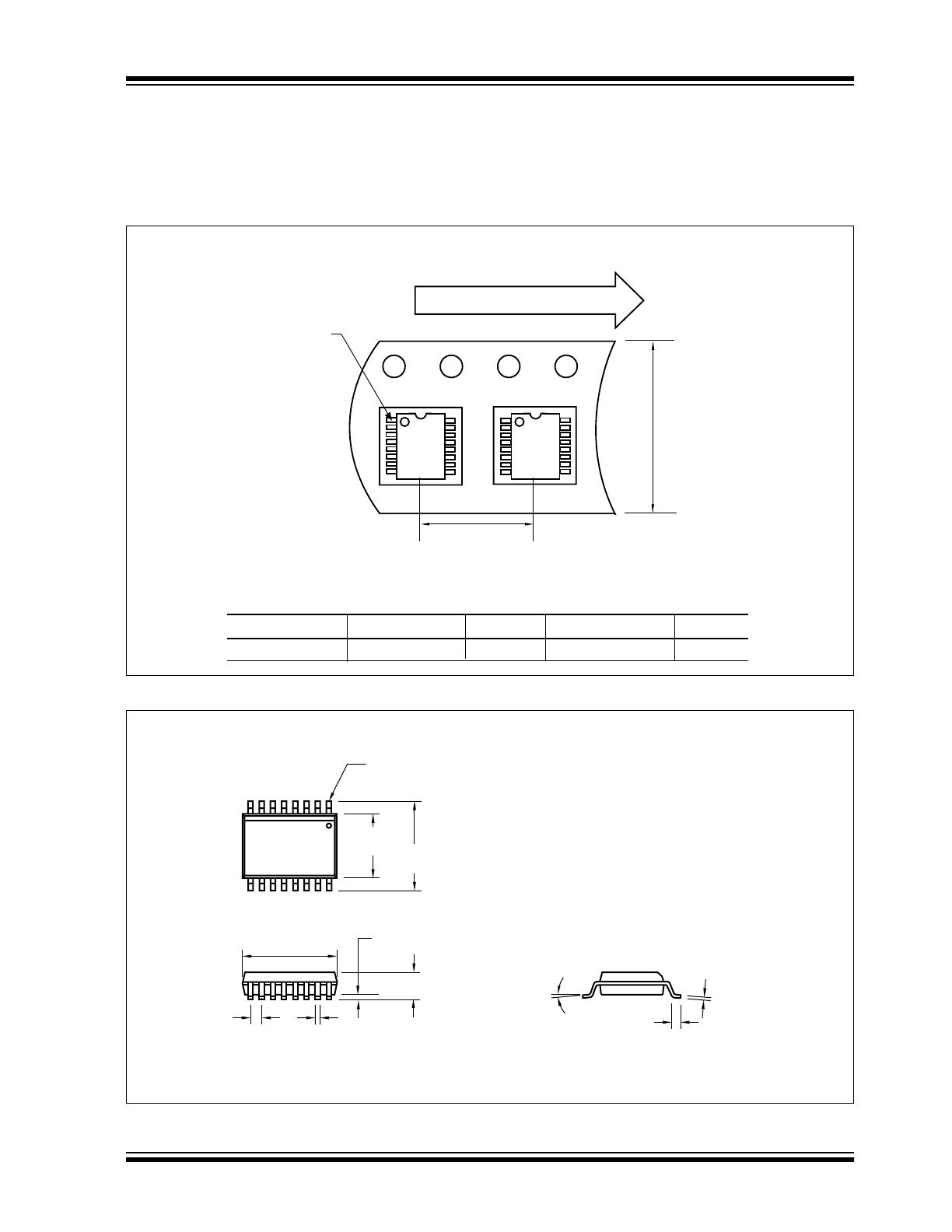
PACKAGING INFORMATION
6.1
Package Marking Information
Package marking data not available at this time.
6.2
Taping Form
6.3
Package Dimensions
Component Taping Orientation for 16-Pin QSOP (Narrow) Devices
PIN 1
User Direction of Feed
Standard Reel Component Orientation
for TR Suffix Device
W
P
Package
Carrier Width (W)
Pitch (P)
Part Per Full Reel
Reel Size
16-Pin QSOP (N)
12 mm
8 mm
2500
13 in
Carrier Tape, Reel Size, Number of Components Per Reel and Reel Size
8
°
MAX.
PIN 1
.157 (3.99)
.150 (3.81)
.196 (4.98)
.189 (4.80)
.012 (0.31)
.008 (0.21)
.010 (0.25)
.004 (0.10)
.069 (1.75)
.053 (1.35)
.010 (0.25)
.007 (0.19)
.050 (1.27)
.016 (0.41)
.244 (6.20)
.228 (5.80)
.025
(0.635)
TYP.
16-Pin QSOP (Narrow)
Dimensions: inches (mm)

TC1030
DS21341B-page 10
2002 Microchip Technology Inc.
NOTES: