
2002 Microchip Technology Inc.
DS21347B-page 1
Features
• Combines Two Op Amps, Two Comparators and
a Voltage Reference in a Single Package
• Optimized for Single-Supply Operation
• Small Package: 16-Pin QSOP
• Ultra Low Input Bias Current: Less than 100pA
• Low Quiescent Current: Operating 16
µ
A (Typ.)
Shutdown 6
µ
A (Typ.)
• Rail-to-Rail Inputs and Outputs
• Operates Down to V
DD
= 1.8V
• Reference and One Comparator Remain Active in
Shutdown to Provide Supervisory Functions
Applications
• Power Management Circuits
• Battery Operated Equipment
• Consumer Products
• Replacements for Discrete Components
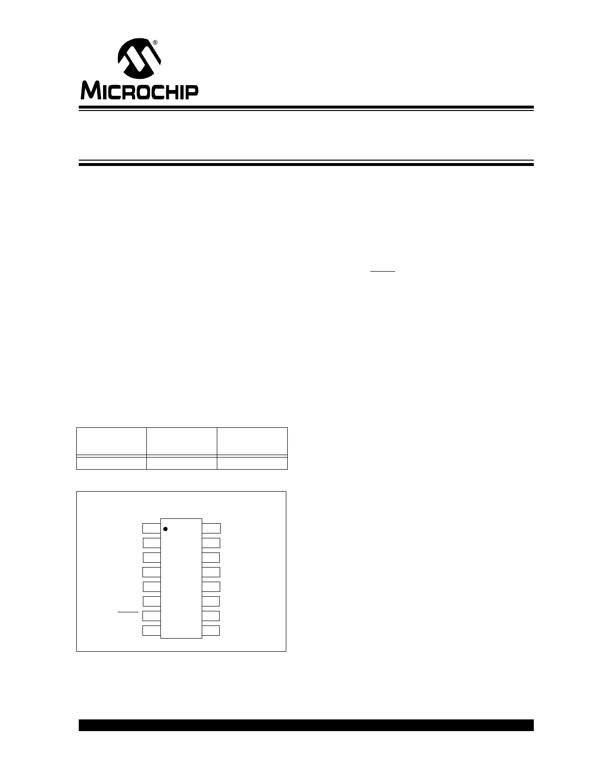
Device Selection Table
Package Type
General Description
The TC1043 is a mixed-function device combining two
general purpose op amps, two general purpose com-
parators, and a voltage reference in a single 16-Pin
package.
This increased integration allows the user to replace
two or three packages, saving space, lowering supply
current, and increasing system performance. A shut-
down input, SHDN, disables the op amps and one of
the comparators, placing their outputs in a high-imped-
ance state. The reference and one comparator stay
active in shutdown mode. Standby power consumption
is typically 6
µ
A. Both the op amps and comparators
have rail-to-rail inputs and outputs which allows opera-
tion from low supply voltages with large input and out-
put signal swings.
Packaged in a 16-Pin QSOP, the TC1043 is ideal for
applications requiring high integration, small size and
low power.
Part Number
Package
Temperature
Range
TC1043CEQR
16-Pin QSOP
-40°C to +85°C
V
DD
TC1043
_EQR
1
2
3
4
16
15
14
A1
IN+
A1
IN–
A2
IN+
A1
OUT
A2
OUT
A2
IN–
C1
IN+
C1
IN–
C2
IN+
C2
IN–
C1
OUT
C2
OUT
SHDN
V
SS
V
REF
5
6
7
8
13
12
11
10
9
16-Pin QSOP
TC1043
Linear Building Block – Low Power Voltage Reference with
Dual Op Amp, Dual Comparator, and Shutdown Mode
TC1043
DS21347B-page 2
2002 Microchip Technology Inc.
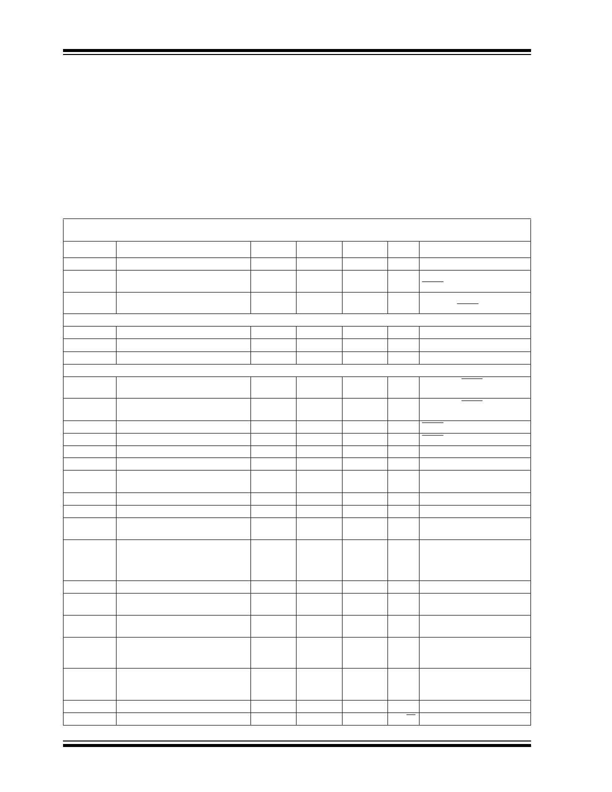
1.0
ELECTRICAL
CHARACTERISTICS
ABSOLUTE MAXIMUM RATINGS*
Supply Voltage ......................................................6.0V
Voltage on Any Pin ........... (V
SS
– 0.3V) to (V
DD
+0.3V)
Junction Temperature....................................... +150°C
Operating Temperature Range............. -40°C to +85°C
Storage Temperature Range .............. -55°C to +150°C
*Stresses above those listed under “Absolute Maximum
Ratings” may cause permanent damage to the device.
These are stress ratings only and functional operation of the
device at these or any other conditions above those indi-
cated in the operation sections of the specifications is not
implied. Exposure to Absolute Maximum Rating conditions
for extended periods my affect device reliability.
TC1043 ELECTRICAL SPECIFICATIONS
Electrical Characteristics: Typical values apply at 25°C and V
DD
= 3V. Minimum and maximum values apply for T
A
= -40° to
+ 85°C, and V
DD
= 1.8V to 5.5V, unless otherwise specified.
Symbol
Parameter
Min.
Typ
Max
Units
Test Conditions
V
DD
Supply Voltage
1.8
—
5.5
V
I
Q
Supply Current Operating
—
16
30
µ
A
All outputs unloaded,
SHDN = V
DD
I
SHDN
Supply Current, Shutdown
—
6
10
µ
A
CMPTR2 and V
REF
Outputs
unloaded, SHDN = V
SS
Shutdown Input
V
IH
Input High Threshold
80% V
DD
—
—
V
V
IL
Input Low Threshold
—
—
20% V
DD
V
I
SI
Shutdown Input Current
—
—
±100
nA
Op Amps
T
SEL
Select Time
—
15
—
µ
sec
(V
OUT
from SHDN = V
IH
)
R
L
= 10k
Ω
to V
SS
T
DESEL
Deselect Time
—
100
—
nsec
(V
OUT
from SHDN = V
IL
)
R
L
= 10k
Ω
to V
SS
R
OUT
(SD)
Output Resistance in Shutdown
20
—
—
M
Ω
SHDN = V
SS
C
OUT
(SD)
Output Capacitance in Shutdown
—
—
6
pF
SHDN = V
SS
A
VOL
Large Signal Voltage Gain
—
100
—
V/mV
R
L
= 10k
Ω
, V
DD
= 5V
V
ICMR
Common Mode Input Voltage Range
V
SS
- 0.2
—
V
DD
+ 0.2
V
V
OS
Input Offset Voltage
±100
±0.3
±500
±1.5
µ
V
mV
V
DD
= 3V, V
CM
= 1.5V, T
A
=
25°C, T
A
= -40°C to 85°C
I
B
Input Bias Current
-100
50
100
pA
T
A
= 25°C, V
CM
= V
DD
to V
SS
V
OS(DRIFT)
Input Offset Voltage Drift
—
±4
—
µ
V/°C
V
DD
= 3V, V
CM
= 1.5V
GBWP
Gain-Bandwidth Product
—
90
—
kHz
V
DD
= 1.8V to 5.5V
V
O
= V
DD
to V
SS
SR
Slew Rate
—
35
—
mV/
µ
sec
C
L
= 100pF
R
L
= 1M
Ω
to GND
Gain = 1
V
IN
= V
SS
to V
DD
V
OUT
Output Signal Swing
V
SS
+ 0.05
—
V
SS
- 0.05
V
R
L
= 10k
Ω
CMRR
Common Mode Rejection Ratio
70
—
—
dB
T
A
= 25°C, V
DD
= 5V
V
CM
= V
DD
to V
SS
PSRR
Power Supply Rejection Ratio
80
—
—
dB
T
A
= 25°C, V
CM
= V
SS
V
DD
= V
DD
to V
SS
I
SRC
Output Source Current
3
—
—
mA
IN+ = V
DD
, IN- = V
SS
Output Shorted to V
SS
V
DD
= 1.8V, Gain = 1
I
SINK
Output Sink Current
4
—
—
mA
IN+ = V
SS
, IN- = V
DD
Output Shorted to V
DD
V
DD
= 1.8V, Gain = 1
En
Input Noise Voltage
—
10
—
µ
V
PP
0.1Hz to 10Hz
en
Input Noise Voltage Density
—
125
—
nV/
√
Hz 1kHz
2002 Microchip Technology Inc.
DS21347B-page 3
TC1043
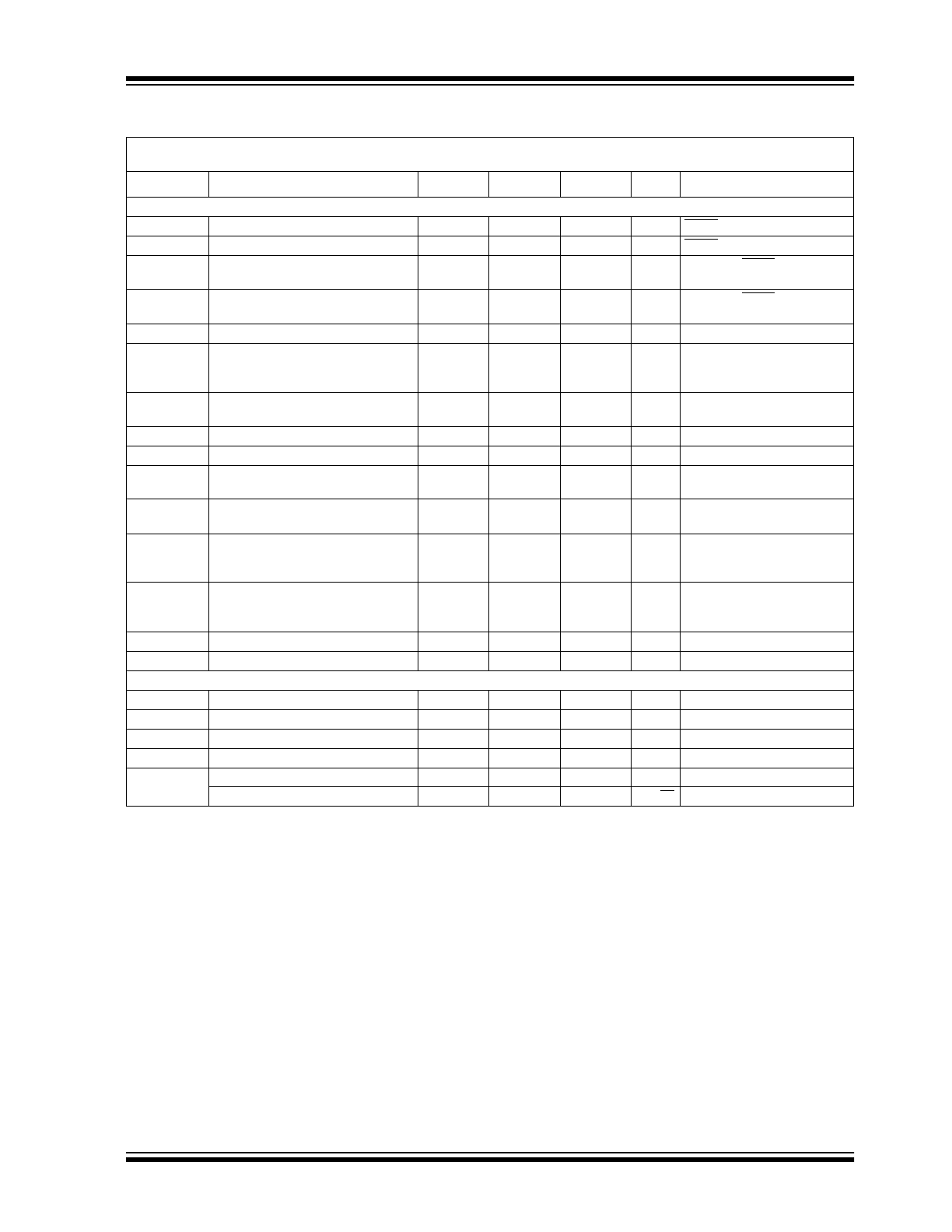
TC1043 ELECTRICAL SPECIFICATIONS (CONTINUED)
Electrical Characteristics: Typical values apply at 25°C and V
DD
= 3V. Minimum and maximum values apply for T
A
= - 40° to + 85°C, and
V
DD
= 1.8V to 5.5V, unless otherwise specified.
Symbol
Parameter
Min.
Typ
Max
Units
Test Conditions
Comparators
R
OUT
(SD)
Output Resistance in Shutdown
20
—
—
M
Ω
SHDN = V
SS
C
OUT
(SD)
Output Capacitance in Shutdown
—
—
5
pF
SHDN = V
SS
T
SEL
Select Time (For Valid Output)
—
20
—
µ
sec
V
OUT
from SHDN = V
IH
R
L
=10k
Ω
to V
SS
T
DESEL
Deselect Time
—
500
—
nsec
V
OUT
from SHDN = V
IL
R
L
=10k
Ω
to V
SS
V
ICMR
Common Mode Input Voltage Range
V
SS
– 0.2
—
V
DD
+ 0.2
V
V
OS
Input Offset Voltage
–5
–5
—
+5
+5
mV
V
DD
= 3V, V
CM
= 1.5V
T
A
= 25°C
T
A
= -40°C to 85°C
I
B
Input Bias Current
—
—
±100
pA
T
A
= 25°C,
IN+, IN- = V
DD
to V
SS
V
OH
Output High Voltage
V
DD
– 0.3
—
—
V
R
L
= 10k
Ω
to V
SS
V
OL
Output Low Voltage
—
—
0.3
V
R
L
= 10k
Ω
to V
DD
CMRR
Common Mode Rejection Ratio
66
—
—
dB
T
A
= 25°C, V
DD
= 5V
V
CM
= V
DD
to V
SS
PSRR
Power Supply Rejection Ratio
60
—
—
dB
T
A
= 25°C, V
CM
= 1.2V
V
DD
= 1.8V to 5V
I
SRC
Output Source Current
1
—
—
mA
IN+ = V
DD
, IN- = V
SS
Output Shorted to V
SS
V
DD
= 1.8V
I
SINK
Output Sink Current
2
—
—
mA
IN+ = V
SS
, IN- = V
DD,
Output Shorted to V
DD
V
DD
= 1.8V
t
PD1
Response Time
—
4
—
µ
sec
100mV Overdrive, C
L
= 100pF
t
PD2
Response Time
—
6
—
µ
sec
10mV Overdrive, C
L
= 100pF
Voltage Reference
V
REF
Reference Voltage
1.176
1.200
1.224
V
I
REF(SOURCE)
Source Current
50
—
—
µ
A
I
REF(SINK)
Sink Current
50
—
—
µ
A
C
L(REF)
Load Capacitance
—
—
100
pF
N
VREF
Voltage Noise
—
20
—
µ
V
RMS
100Hz to 100kHz
Noise Density
—
1.0
—
µ
V/
√
Hz 1kHz

TC1043
DS21347B-page 4
2002 Microchip Technology Inc.
2.0
PIN DESCRIPTION
The descriptions of the pins are listed in Table 2-1.
TABLE 2-1:
PIN FUNCTION TABLE
Pin Number
Symbol
Description
1
A1
IN+
Op Amp Non-Inverting Input
2
A1
IN-
Op Amp Inverting Input
3
A2
IN+
Op Amp Non-Inverting Input
4
A2
IN-
Op Amp Inverting Input
5
C1
OUT
Comparator Output
6
C2
OUT
Comparator Output
7
SHDN
Shutdown Input
8
V
SS
Negative Power Supply
9
V
REF
Voltage Reference Output
10
C2
IN-
Comparator Inverting Input
11
C2
IN+
Comparator Non-Inverting Input
12
C1
IN-
Comparator Inverting Input
13
C1
IN+
Comparator Non-Inverting Input
14
A2
OUT
Op Amp Output
15
A1
OUT
Op Amp Output
16
V
DD
Positive Power Supply

2002 Microchip Technology Inc.
DS21347B-page 5
TC1043
3.0
DETAILED DESCRIPTION
The TC1043 is one of a series of very low power, linear
building block products targeted at low voltage, single
supply applications. The TC1043 minimum operating
voltage is 1.8V and typical supply current is only 20
µ
A
(fully enabled). It combines two comparators, two op
amps and a voltage reference in a single package. A
shutdown mode is incorporated for easy adaptation to
system power management schemes. During shut-
down, all but one comparator and the voltage reference
are disabled (i.e. powered down with their respective
outputs at high impedance). The “still awake” compar-
ator and voltage reference can be used as a wake-up
timer, power supply monitor, LDO controller or other
continuous duty circuit function.
3.1
Comparators
The TC1043 contains two comparators. The compara-
tors input range extends beyond both supply voltages
by 200mV and the outputs will swing to within several
millivolts of the supplies, depending on the load current
being driven.
The comparators exhibit a propagation delay and sup-
ply current which are largely independent of supply
voltage. The low input bias current and offset voltage
make them suitable for high impedance precision appli-
cations.
Comparator CMPTR1 is disabled during shutdown and
has a high impedance output. Comparator CMPTR2
remains active.
3.2
Operational Amplifiers
The TC1043 contains two rail-to-rail op amps. The
amplifiers’ input range extends beyond both supplies
by 200mV and the outputs will swing to within several
millivolts of the supplies depending on the load current
being driven.
The amplifier design is such that large signal gain, slew
rate and bandwidth are largely independent of supply
voltage. The low input bias current and offset voltage of
the TC1043 make it suitable for precision applications.
Both op amps are disabled during shutdown and have
high output impedance.
3.3
Voltage Reference
A 2.0% tolerance, internally biased, 1.20V bandgap
voltage reference is included in the TC1043. It has a
push-pull output capable of sourcing and sinking at
least 50
µ
A. The voltage reference remains fully
enabled during shutdown.
3.4
Shutdown Input
SHDN at V
IL
disables both op amps and one compara-
tor. The SHDN input cannot be allowed to float. When
not used, connect it to V
DD
. The disabled comparator’s
output and the two disabled op amp outputs are in a
high impedance state when shutdown is active. The
disabled comparator’s inputs and the two disabled op
amp inputs can be driven from rail-to-rail by an external
voltage when the TC1043 is in shutdown. No latch-up
will occur when the device is driven to its enabled state
when SHDN is set to V
IH
.
TC1043
DS21347B-page 6
2002 Microchip Technology Inc.
4.0
TYPICAL APPLICATIONS
The TC1043 lends itself to a wide variety of applica-
tions, particularly in battery powered systems. It typi-
cally
finds
application
in
power
management,
processor supervisory, and interface circuitry.
4.1
Wake-Up Timer
Many microcontrollers have a low power “sleep” mode
that significantly reduces their supply current. Typically,
the microcontroller is placed in this mode via a software
instruction, and returns to a fully enabled state upon
reception of an external signal (“wake-up”). The wake-
up signal is usually supplied by a hardware timer. Most
system applications demand that this timer have a long
duration (typically seconds or minutes), and consume
as little supply current as possible.
The circuit shown in Figure 4-1 is a wake-up timer
made from comparator CMPTR2. (CMPTR2 is used
because the wake-up timer must operate when SHDN
is active.) Capacitor C1 charges through R1 until a volt-
age equal to V
R
is reached, at which point the WAKE-
UP is driven active. Upon wake-up, the microcontroller
resets the timer by forcing a logic low on a dedicated,
open drain I/O port pin. This discharges C1 through R4
(the value of R4 is chosen to limit the maximum current
sunk by the I/O port pin). With a 3V supply, the circuit
as shown consumes typically 6
µ
A and furnishes a
nominal timer duration of 25 seconds.
4.2
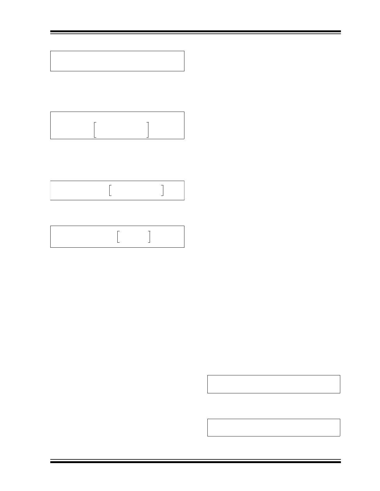
Precision Battery Monitor
Figure 4-2 is a precision battery low/battery dead mon-
itoring circuit. Typically, the battery low output warns
the user that a battery dead condition is imminent. Bat-
tery dead typically initiates a forced shutdown to pre-
vent operation at low internal supply voltages (which
can cause unstable system operation).
The circuit of Figure 4-2 uses a single TC1043 (one op
amp is unused) and only six external resistors. AMP 1
is a simple buffer, while CMPTR1 and CMPTR2 provide
precision voltage detection using V
R
as a reference.
Resistors R2 and R4 set the detection threshold for
BATTLOW, while resistors R1 and R3 set the detection
threshold for BATTFAIL. The component values shown
assert BATTLOW at 2.2V (typical) and BATTFAIL at
2.0V (typical). Total current consumed by this circuit is
typically 22
µ
A at 3V. Resistors R5 and R6 provide hys-
teresis for comparators CMPTR1
and
CMPTR2
respectively.
4.3
Dual LDO with Shutdown
Figure 4-3 shows a portion of a TC1043 configured as
a dual low dropout regulator with shutdown. AMP1 and
AMP2 are independent error amplifiers that use V
R
as
a reference. Resistors RA
1
, RB
1
, RA
2
and RB
2
set the
feedback around the amplifiers and therefore deter-
mine the output voltage settings (please see equation
in the figure). RA
1
, RB
1
, RA
2
and RB
2
can have large
ohmic values (i.e. 100’s of k
Ω
) to minimize supply cur-
rent.
Using the 2N2222 output transistors as shown, these
regulators exhibit low dropout operation. For example,
with V
OUT
= 3.0V, the typical dropout voltage is only
50mV at an output current of 50mA. The unused com-
parators can be used in conjunction with this circuit as
power-on reset or low voltage detectors for a complete
LDO solution at a very low installed cost.
4.4
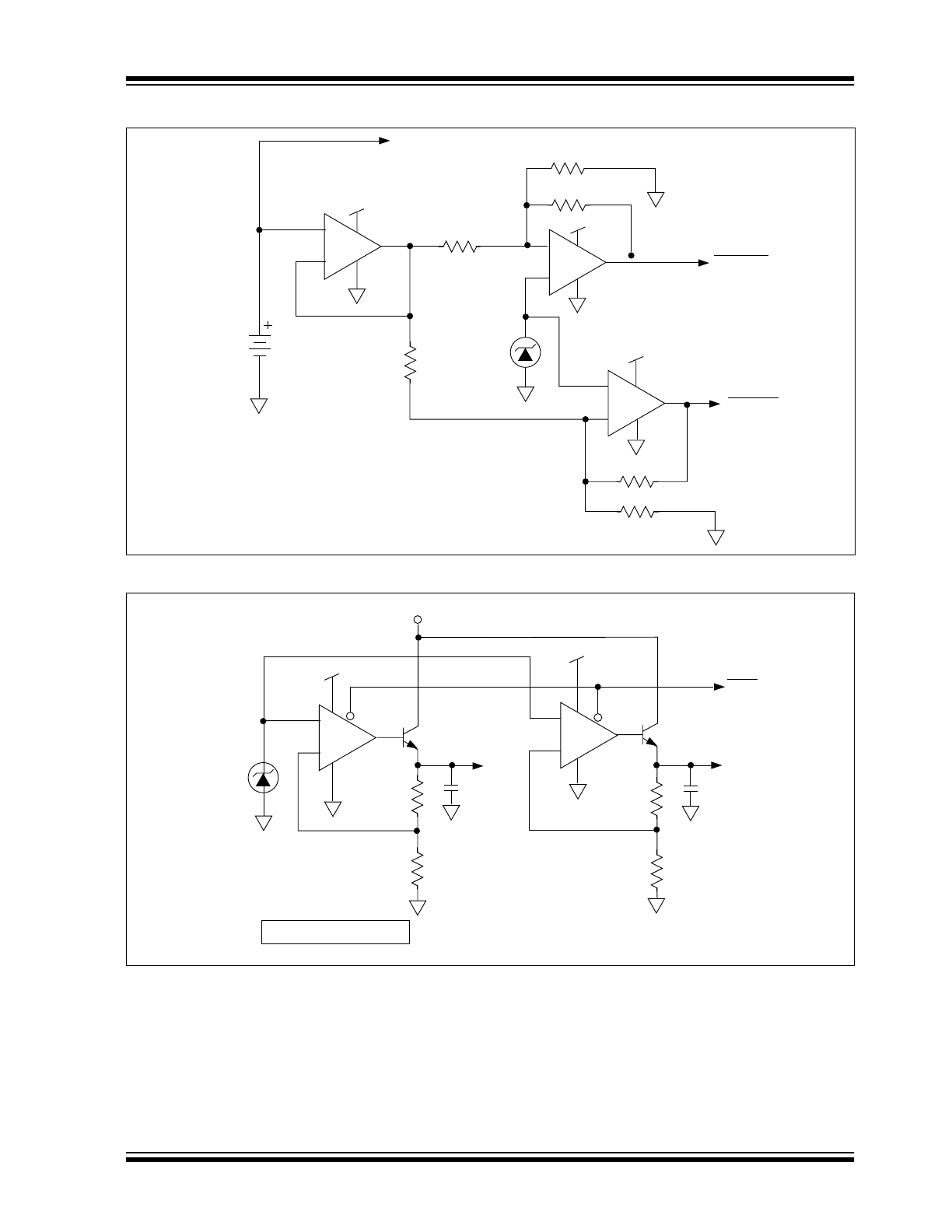
External Hysteresis
Hysteresis can be set externally with two resistors
using positive feedback techniques (see Figure 4-3).
The design procedure for setting external comparator
hysteresis is as follows:
1.
Choose the feedback resistor R
C
. Since the
input bias current of the comparator is at most
100pA, the current through R
C
can be set to
100nA (i.e. 1000 times the input bias current)
and retain excellent accuracy. The current
through R
C
at the comparator’s trip point is V
R
/
R
C
where V
R
is a stable reference voltage.
FIGURE 4-1:
WAKE-UP TIMER
2.
Determine the hysteresis voltage (V
HY
) between
the upper and lower thresholds.
3.
Calculate R
A
as follows:
WAKE-UP
R1
5M
R4
C1
10µF
V
DD
V
DD
V
R
I/O*
*Open Drain Port Pin
Microcontroller
CMPTR2
TC1043
+
–
2002 Microchip Technology Inc.
DS21347B-page 7
TC1043
EQUATION 4-1:
4.
Choose the rising threshold voltage for V
SRC
(V
THR
).
5.
Calculate R
B
as follows:
EQUATION 4-2:
6.
Verify the threshold voltages with these formu-
las:
V
SRC
rising:
EQUATION 4-3:
V
SRC
falling:
EQUATION 4-4:
4.5
32.768kHz ‘Time Of Day Clock’
Crystal Controlled Oscillator
A very stable oscillator driver can be designed by using
a crystal resonator as the feedback element. Figure 4-
5 shows a typical application circuit using this tech-
nique to develop a clock driver for a Time-Of-Day
(TOD) clock chip. The value of R
A
and R
B
determines
the DC voltage level at which the comparator trips; in
this case one-half of V
DD
. The RC time constant of R
C
and C
A
should be set several times greater than the
crystal oscillator’s period, which will ensure a 50% duty
cycle by maintaining a DC voltage at the inverting com-
parator input equal to the absolute average of the out-
put signal.
4.6
Non-Retriggerable One Shot Multi-
vibrator
Using two comparators, a non-retriggerable, one shot
multi-vibrator can be designed using the circuit config-
uration of Figure 4-6. A key feature of this design is that
the pulse width is independent of the magnitude of the
supply voltage because the charging voltage and the
intercept voltage are a fixed percentage of V
DD
. In addi-
tion, this one shot is capable of pulse width with as
much as a 99% duty cycle and exhibits input lockout to
ensure that the circuit will not re-trigger before the out-
put pulse has completely timed out. The trigger level is
the voltage required at the input to raise the voltage at
node A higher than the voltage at node B, and is set by
the resistive divider R4 and R10 and the impedance
network composed of R1, R2 and R3. When the one
shot has been triggered, the output of CMPTR2 is high,
causing the reference voltage at the non-inverting input
of CMPTR1 to go to V
DD
. This prevents any additional
input pulses from disturbing the circuit until the output
pulse has timed out.
The value of the timing capacitor C1 must be small
enough to allow CMPTR1 to discharge C1 to a diode
voltage before the feedback signal from CMPTR2
(through R10) switches CMPTR1 to its high state and
allows C1 to start an exponential charge through R5.
Proper circuit action depends upon rapidly discharging
C1 through the voltage set by R6, R9 and D2 to a final
voltage of a small diode drop. Two propagation delays
after the voltage on C1 drops below the level on the
non-inverting input of CMPTR2, the output of CMPTR1
switches to the positive rail and begins to charge C1
through R5. The time delay which sets the output pulse
width results from C1 charging to the reference voltage
set by R6, R9 and D2, plus four comparator propaga-
tion delays. When the voltage across C1 charges
beyond the reference, the output pulse returns to
ground and the input is again ready to accept a trigger
signal.
4.7
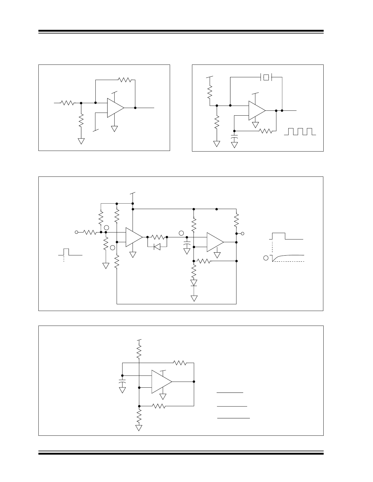
Oscillators and Pulse Width
Modulators
Microchip’s linear building block comparators adapt
well to oscillator applications for low frequencies (less
than 100kHz). Figure 4-7 shows a symmetrical square
wave generator using a minimum number of compo-
nents. The output is set by the RC time constant of R4
and C1, and the total hysteresis of the loop is set by R1,
R2 and R3. The maximum frequency of the oscillator is
limited only by the large signal propagation delay of the
comparator in addition to any capacitive loading at the
output which degrades the slew rate.
To analyze this circuit, assume that the output is initially
high. For this to occur, the voltage at the inverting input
must be less than the voltage at the non-inverting input.
Therefore, capacitor C1 is discharged. The voltage at
the non-inverting input (V
H
) is:
EQUATION 4-5:
where, if R1 = R2 = R3, then:
EQUATION 4-6:
R
A
R
C
V
HY
V
DD
-----------
=
R
B
1
V
THR
V
R
R
A
×
---------------------
1
R
A
-------
–
1
R
C
-------
–
-----------------------------------------------------------
=
V
TH R
V
R
(
)
R
A
(
)
1
R
A
-------
1
R
B
-------
1
R
C
-------
+
+
=
V
THF
V
THR
R
A
V
D D
×
(
)
R
C
------------------------------
–
=
V
H
R2 V
DD
(
)
R2
R1 R3
||
(
)
+
[
]
---------------------------------------------
=
V
H
2 V
DD
(
)
3
-------------------
=

TC1043
DS21347B-page 8
2002 Microchip Technology Inc.
Capacitor C1 will charge up through R4. When the volt-
age at the comparator’s inverting input is equal to V
H
,
the comparator output will switch. With the output at
ground potential, the value at the non-inverting input
terminal (V
L
) is reduced by the hysteresis network to a
value given by:
EQUATION 4-7:
Using the same resistors as before, capacitor C1 must
now discharge through R4 toward ground. The output
will return to a high state when the voltage across the
capacitor has discharged to a value equal to V
L
. The
period of oscillation will be twice the time it takes for the
RC circuit to charge up to one-half its final value. The
period can be calculated from:
EQUATION 4-8:
The frequency stability of this circuit should only be a
function of the external component tolerances.
Figure 4-8 shows the circuit for a pulse width modulator
circuit. It is essentially the same as in Figure 4-7 with
the addition of an input control voltage. When the input
control voltage is equal to one-half V
DD
, operation is
basically the same as described for the free-running
oscillator. If the input control voltage is moved above or
below one-half V
DD
, the duty cycle of the output square
wave will be altered. This is because the addition of the
control voltage at the input has now altered the trip
points. The equations for these trip points are shown in
Figure 4-8 (see V
H
and V
L
).
Pulse width sensitivity to the input voltage variations
can be increased by reducing the value of R6 from
10k
Ω
and conversely, sensitivity will be reduced by
increasing the value of R6. The values of R1 and C1
can be varied to produce the desired center frequency.
4.8
Voice Band Receive Filter
The majority of spectral energy for human voices is
found to be in a 2.7kHz frequency band from 300Hz to
3kHz. To properly recover a voice signal in applications
such as radios, cellular phones, and voice pagers, a
low power bandpass filter that is matched to the human
voice spectrum can be implemented using MIcrochip’s
CMOS op amps. Figure 4-9 shows a unity gain multi-
pole Butterworth filter with ripple less than 0.15dB in
the human voice band. The lower 3dB cut-off frequency
is 70Hz (single order response), while the upper cut-off
frequency is 3.5kHz (fourth order response).
4.9
Supervisory Audio Tone (SAT)
Filter for Cellular
Supervisory Audio Tones (SAT) provide a reliable
transmission path between cellular subscriber units
and base stations. The SAT tone functions much like
the current/voltage used in land line telephone systems
to indicate that a phone is off the hook. The SAT tone
may be one of three frequencies: 5970, 6000 or
6030Hz. A loss of SAT implies that channel conditions
are impaired and if SAT is interrupted for more than 5
seconds a cellular call is terminated.
Figure 4-10 shows a high Q (30) second order SAT
detection bandpass filter using Microchip’s CMOS op
amp architecture. This circuit nulls all frequencies
except the three SAT tones of interest.
V
L
V
DD
3
-----------
=
1
FREQ
-----------------
2 0.694
(
)
R4
(
)
C1
(
)
=
2002 Microchip Technology Inc.
DS21347B-page 9
TC1043
FIGURE 4-2:
PRECISION BATTERY MONITOR
FIGURE 4-3:
DUAL LOW DROPOUT REGULATOR
R2, 330k, 1%
R4, 470k, 1%
R5, 7.5M
R6, 7.5M
R3, 470k, 1%
R1, 270k, 1%
VR
VDD
To System DC/DC
Converter
3V
ALKALINE
BATTFAIL
BATTLOW
CMPTR1
+
–
CMPTR2
+
–
AMP1
+
–
VDD
VDD
TC1043
V
R
VIN
V
OUT1
C1, 1µF
C2, 1µF
2N2222
VOUT = VR x (R
A
+ R
B
)/R
B
RA
1
RB
1
RA
2
RB
2
2N2222
TC1043
SHDN
V
OUT2
AMP2
+
–
AMP1
+
–
V
DD
V
DD
TC1043
DS21347B-page 10
2002 Microchip Technology Inc.
FIGURE 4-4:
COMPARATOR
EXTERNAL HYSTERESIS
CONFIGURATION
FIGURE 4-5:
32.768 KHZ “TIME-OF-
DAY” CLOCK
OSCILLATOR
FIGURE 4-6:
NON-RETRIGGERABLE MULTI-VIBRATOR
FIGURE 4-7:
SQUARE WAVE GENERATOR
+
–
V
R
V
DD
V
OUT
V
SRC
R
A
R
B
R
C
TC1043
Comparator
+
–
V
DD
V
OUT
VDD
R
B
150k
R
A
150k
R
C
1M
C
A
100 pF
32.768 kHz
T
PER
= 30.52 µsec
TC1043
Comparator
+
–
+
–
V
DD
CMPTR1
CMPTR2
In
In
Out
Out
R3
1M
R4
1M
R6
562k
R7
1M
R2
100k
R1
100k
R8
D2
D1
10M
R9
243k
R5
10M
C1
100 pF
R10
61.9k
A
B
C
GND
t0
C
GND
V
DD
GND
V
DD
TC1025
TC1043
V
DD
+
–
R1
100k
V
DD
R4
R3
100k
R2
100k
C1
V
H
=
R2 (V
DD
)
R2 + (R1||R3)
V
L
=
(V
DD
) (R2||R3)
R1 + (R2||R3)
FREQ = 1
2(0.694)(R4)(C1)
TC1043
Comparator