
2002 Microchip Technology Inc.
DS21725B-page 1
Features
• Combines Low-Power Op Amp, Comparator and
Voltage Reference in a Single Package
• Optimized for Single Supply Operation
• Small Packages: 8-Pin MSOP, 8-Pin SOIC,
8-Pin PDIP
• Ultra Low Input Bias Current: Less than 100pA
• Low Quiescent Current: 12
µ
A (Typ.)
• Rail-to-Rail Inputs and Outputs
• Operates Down to V
DD
= 1.8V, Min
Applications
• Power Management Circuits
• Battery Operated Equipment
• Consumer Products
Device Selection Table
Package Types
General Description
The TC1026 is a mixed-function device combining a
general-purpose op amp, comparator and voltage
reference in a single 8-pin package. This increased
integration allows the user to replace two or three
packages, which saves space, lowers supply current
and increases system performance.
Both the op amp and comparator have rail-to-rail inputs
and outputs which allows operation from low supply
voltages with large input and output swings. The
TC1026 is optimized for low voltage (V
DD
= 1.8V), low
supply current (12
µ
A typ) operation.
Packaged in a space-saving 8-Pin MSOP, the TC1026
consumes half the board area of an 8-Pin SOIC and is
ideal for applications requiring high integration, small
size and low power. It is also available in 8-Pin SOIC
and 8-Pin PDIP packages.
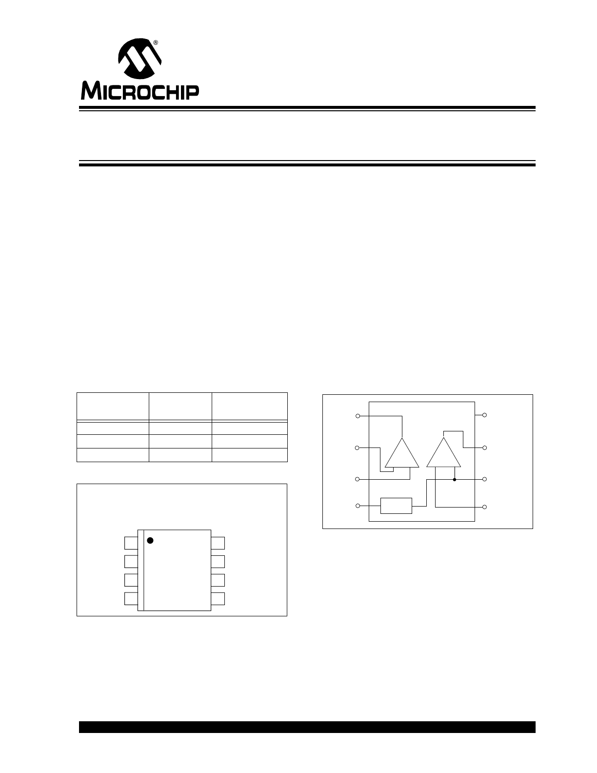
Functional Block Diagram
Part Number
Package
Temperature
Range
TC1026CEPA
8-Pin PDIP
-40°C to +85°C
TC1026CEUA
8-Pin MSOP
-40°C to +85°C
TC1026CEOA
8-Pin SOIC
-40°C to +85°C
REF (CMPIN)
CMPOUT
CMPIN+
AMPIN
AMPIN+
V
SS
AMPOUT
V
DD
1
2
3
4
8
7
6
5
TC1026CEPA
TC1026CEUA
TC1026CEOA
8-Pin PDIP
8-Pin MSOP
8-Pin SOIC
+
-
+
-
TC1026
V
DD
CMPOUT
REF (CMPIN-)
CMPIN+
V
SS
AMPIN+
AMPIN-
AMPOUT
CMP
AMP
Voltage
Reference
1
2
3
4
8
7
6
5
TC1026
Linear Building Block – Low Power Comparator with
Op Amp and Voltage Reference
TC1026
DS21725B-page 2
2002 Microchip Technology Inc.
1.0
ELECTRICAL
CHARACTERISTICS
ABSOLUTE MAXIMUM RATINGS*
Supply Voltage ......................................................6.0V
Package Power Dissipation:
8-Pin PDIP ...............................................730 mW
8-Pin SOIC ...............................................470 mW
8-Pin MSOP .............................................320 mW
Voltage on Any Pin .......... (V
SS
– 0.3V) to (V
DD
+ 0.3V)
Junction Temperature....................................... +150°C
Operating Temperature Range............. -40°C to +85°C
Storage Temperature Range .............. -55°C to +150°C
*Stresses above those listed under "Absolute Maximum
Ratings" may cause permanent damage to the device. These
are stress ratings only and functional operation of the device
at these or any other conditions above those indicated in the
operation sections of the specifications is not implied.
Exposure to Absolute Maximum Rating conditions for
extended periods may affect device reliability.
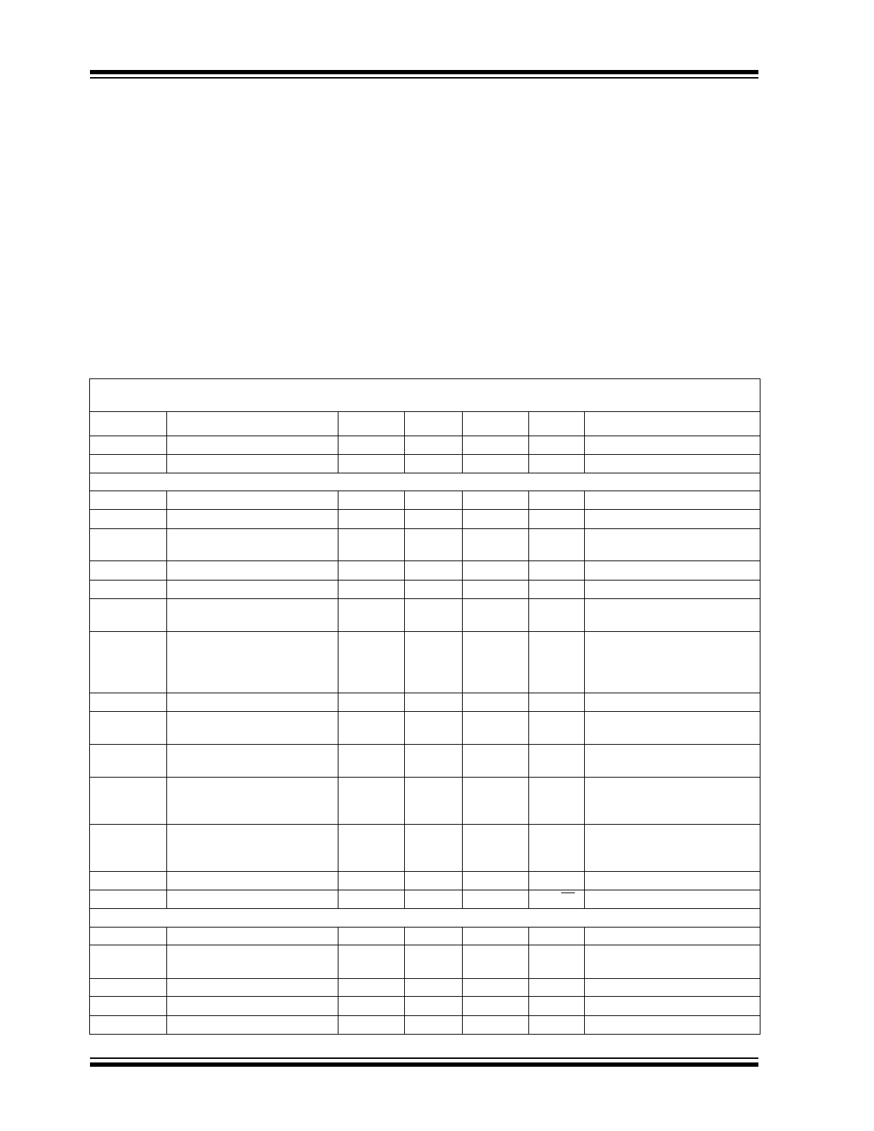
TC1026 ELECTRICAL SPECIFICATIONS
Electrical Characteristics: Typical values apply at 25°C and V
DD
= 3.0V; T
A
= -40° to +85°C, and V
DD
= 1.8V to 5.5V, unless
otherwise specified.
Symbol
Parameter
Min
Typ
Max
Units
Test Conditions
V
DD
Supply Voltage
1.8
—
5.5
V
I
Q
Supply Current
—
12
18
µ
A
All outputs unloaded
Op Amp
A
VOL
Large Signal Voltage Gain
—
100
—
V/mV
R
L
= 10k
Ω,
V
DD
= 5V
V
ICMR
Common Mode Input Range
V
SS
– 0.2
—
V
DD
+ 0.2
V
V
OS
Input Offset Voltage
±100
±0.3
±500
±1.5
µ
V
mV
V
DD
= 3V, V
CM
= 1.5V, T
A
= 25°C
T
A
= -40°C to 85°C
I
B
Input Bias Current
-100
50
100
pA
T
A
= 25°C, V
CM
= V
DD
to V
SS
V
OS (DRIFT)
Input Offset Voltage Drift
—
±4
—
µ
V/°C
V
DD
= 3V, V
CM
= 1.5V
GBWP
Gain-Bandwidth Product
—
90
—
kHz
V
DD
= 1.8V to 5.5V;
V
O
= V
DD
to V
SS
SR
Slew Rate
—
35
—
mV/
µ
sec C
L
= 100pF
R
L
= 1M
Ω
to GND
Gain = 1
V
IN
= V
SS
to V
DD
V
OUT
Output Signal Swing
V
SS
+ 0.05
—
V
DD
– 0.05
V
R
L
= 10k
Ω
CMRR
Common Mode Rejection Ratio
66
—
—
dB
T
A
= 25°C, V
DD
= 5V
V
CM
= V
DD
to V
SS
PSRR
Power Supply Rejection Ratio
80
—
—
dB
T
A
= 25°C, V
CM
= V
SS
V
DD
= 1.8V to 5V
I
SRC
Output Source Current
3
—
—
mA
V
IN
+ = V
DD
, V
IN
- = V
SS
Output Shorted to V
SS
V
DD
= 1.8V, Gain = 1
I
SINK
Output SInk Current
—
125
—
nV/Hz
IN+ = V
SS
, IN- = V
DD
Output Shorted to V
DD
V
DD
= 1.8V, Gain = 1
En
Input Noise Voltage
—
10
—
µ
Vpp
0.1Hz to 10Hz
en
Input Noise Voltage Density
—
125
—
nV/
√
Hz
1kHz
Comparator
V
IR
Input Voltage Range
V
SS
– 0.2
—
V
DD
+ 0.2
V
V
OS
Input Offset Voltage
-5
-5
—
—
+5
+5
mV
V
DD
= 3V, T
A
= 25°C
T
A
= -40°C to 85°C
I
B
Input Bias Current
––
—
±100
pA
T
A
= 25°C, IN+ = V
DD
to V
SS
V
OH
Output High Voltage
V
DD
– 0.3
—
—
V
R
L
= 10k
Ω
to V
SS
V
OL
Output Low Voltage
—
—
0.3
V
R
L
= 10k
Ω
to V
DD
2002 Microchip Technology Inc.
DS21725B-page 3
TC1026
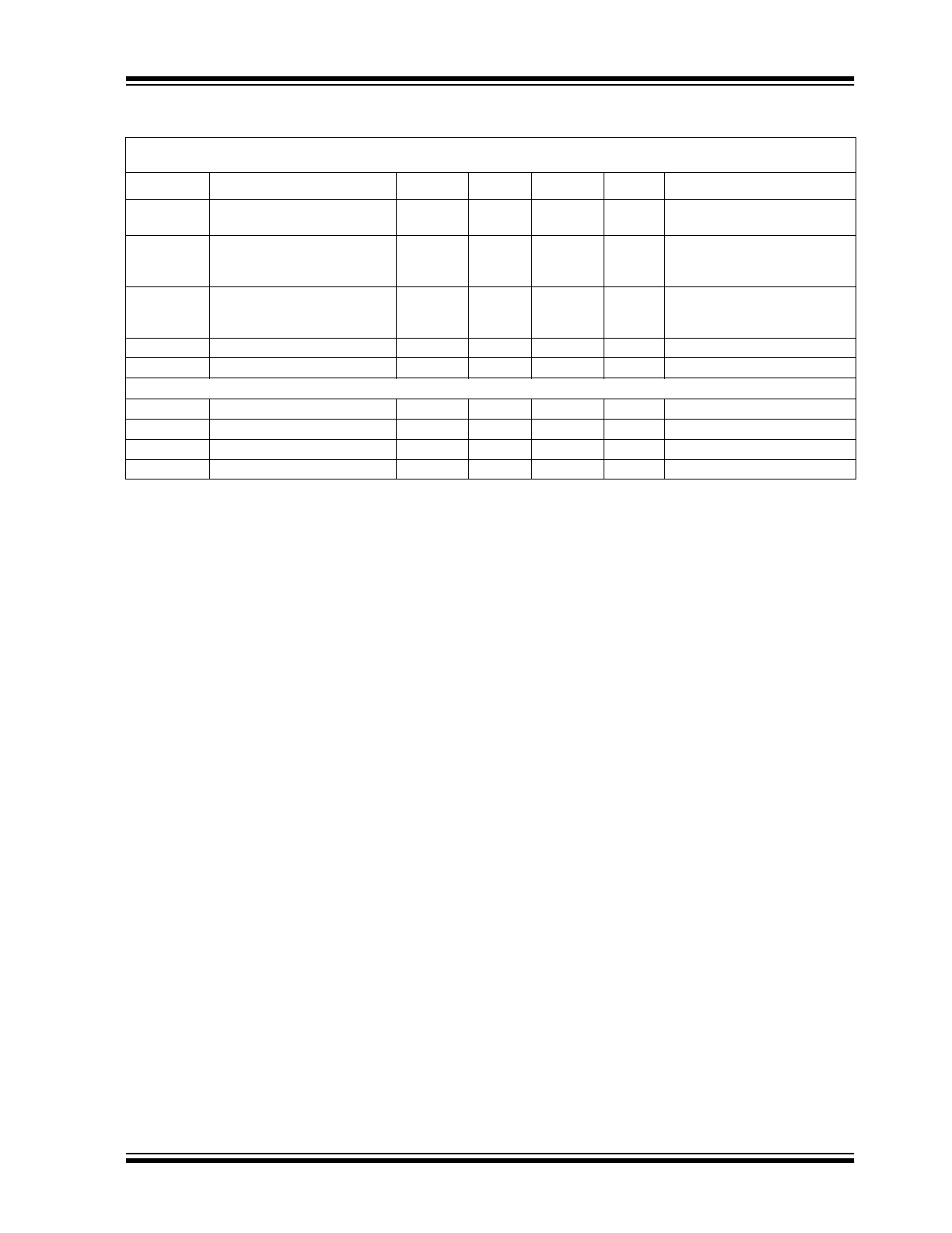
TC1026 ELECTRICAL SPECIFICATIONS (CONTINUED)
Electrical Characteristics: Typical values apply at 25°C and V
DD
= 3.0V; T
A
= -40° to +85°C, and V
DD
= 1.8V to 5.5V, unless
otherwise specified.
Symbol
Parameter
Min
Typ
Max
Units
Test Conditions
PSRR
Power Supply Rejection Ratio
60
—
—
dB
T
A
= 25°C
V
DD
= 1.8V to 5V
I
SRC
Output Source Current
1
—
—
mA
IN+ = V
DD
Output Shorted to V
SS
V
DD
= 1.8V
I
SINK
Output Sink Current
2
—
—
mA
IN+ = V
SS
Output Shorted to V
DD
V
DD
= 1.8V
t
PD1
Response Time
—
4
—
µ
sec
100mV Overdrive, C
L
= 100pF
t
PD2
Response Time
—
6
—
µ
sec
10mV Overdrive, C
L
= 100pF
Voltage Reference
V
REF
Reference Voltage
1.176
1.200
1.221
V
I
REF(SOURCE)
Source Current
50
—
—
µ
A
I
REF(SINK)
Sink Current
50
—
—
µ
A
C
L(REF)
Load Capacitance
—
—
100
pF
TC1026
DS21725B-page 4
2002 Microchip Technology Inc.
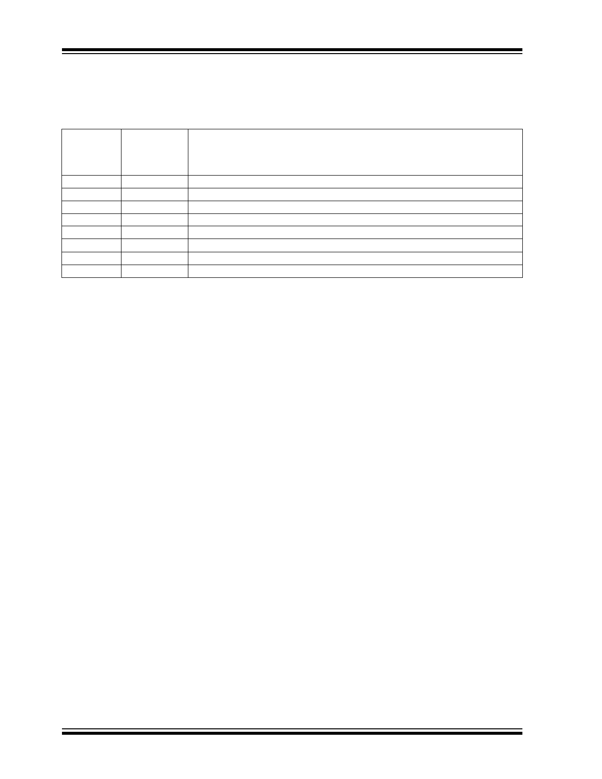
2.0
PIN DESCRIPTION
The description of the pins are listed in Table 2-1.
TABLE 2-1:
PIN FUNCTION TABLE
Pin No.
(8-Pin PDIP)
(8-Pin MSOP)
(8-Pin SOIC)
Symbol
Description
1
AMPOUT
Op amp output.
2
AMPIN-
Inverting op amp input.
3
AMPIN+
Non-inverting op amp input.
4
V
SS
Negative power supply.
5
CMPIN+
Non-inverting comparator input.
6
REF(CMPIN)
Inverting comparator input and voltage reference output voltage.
7
CMPOUT
Comparator output.
8
V
DD
Positive power supply.

2002 Microchip Technology Inc.
DS21725B-page 5
TC1026
3.0
DETAILED DESCRIPTION
The TC1026 is one of a series of very low power, linear
building block products targeted at low voltage, single
supply applications. The TC1026 minimum operating
voltage is 1.8V, and typical supply current is only 12
µ
A.
It combines a comparator, an op amp and a voltage
reference in a single package.
3.1
Comparator
The TC1026 contains one comparator. The compara-
tor’s input range extends beyond both supply voltages
by 200mV and the outputs will swing to within several
millivolts of the supplies depending on the load current
being driven. The inverting input is internally connected
to the output of the reference.
The comparator exhibits propagation delay and supply
current which are largely independent of supply
voltage. The low input bias current and offset voltage
make
it
suitable
for
high
impedance
precision
applications.
3.2
Operational Amplifier
The TC1026 contains one rail-to-rail op amp. The
amplifier’s input range extends beyond both supplies
by 200mV and the outputs will swing to within several
millivolts of the supplies depending on the load current
being driven.
The amplifier design is such that large signal gain, slew
rate and bandwidth are largely independent of supply
voltage. The low input bias current and offset voltage of
the TC1026 make it suitable for precision applications.
3.3
Voltage Reference
A 2.0% tolerance, internally biased, 1.20V bandgap
voltage reference is included in the TC1026. It has a
push-pull output capable of sourcing and sinking at
least 50
µ
A.
4.0
TYPICAL APPLICATIONS
The TC1026 lends itself to a wide variety of
applications, particularly in battery powered systems. It
typically finds application in power management,
processor supervisory and interface circuitry.
4.1
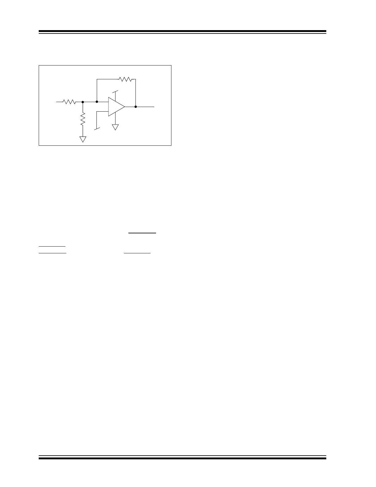
External Hysteresis (Comparator)
Hysteresis can be set externally with three resistors
using positive feedback techniques (see Figure 4-1).
The design procedure for setting external comparator
hysteresis is as follows:
1.
Choose the feedback resistor R
C
. Since the
input bias current of the comparator is at most
100pA, the current through R
C
can be set to
100nA (i.e., 1000 times the input bias current)
and retain excellent accuracy. The current
through R
C
at the comparator’s trip point is V
R
/
R
C
where V
R
is a stable reference voltage.
2.
Determine the hysteresis voltage (V
HY
) between
the upper and lower thresholds.
3.
Calculate R
A
as follows:
EQUATION 4-1:
4.
Choose the rising threshold voltage for V
SRC
(V
THR
).
5.
Calculate R
B
as follows:
EQUATION 4-2:
6.
Verify
the
threshold
voltages
with
these
formulas:
V
SRC
rising:
EQUATION 4-3:
V
SRC
falling:
EQUATION 4-4:
R
A
R
C
V
H Y
V
D D
-----------
=
R
B
1
V
THR
V
R
R
A
×
---------------------
1
R
A
-------
–
1
R
C
-------
–
-----------------------------------------------------------
=
V
TH R
V
R
(
)
R
A
(
)
1
R
A
-------
1
R
B
-------
1
R
C
-------
+
+
=
V
THF
V
THR
R
A
V
DD
×
R
C
-------------------------
–
=
TC1026
DS21725B-page 6
2002 Microchip Technology Inc.
FIGURE 4-1:
COMPARATOR
EXTERNAL HYSTERESIS
CONFIGURATION
4.2
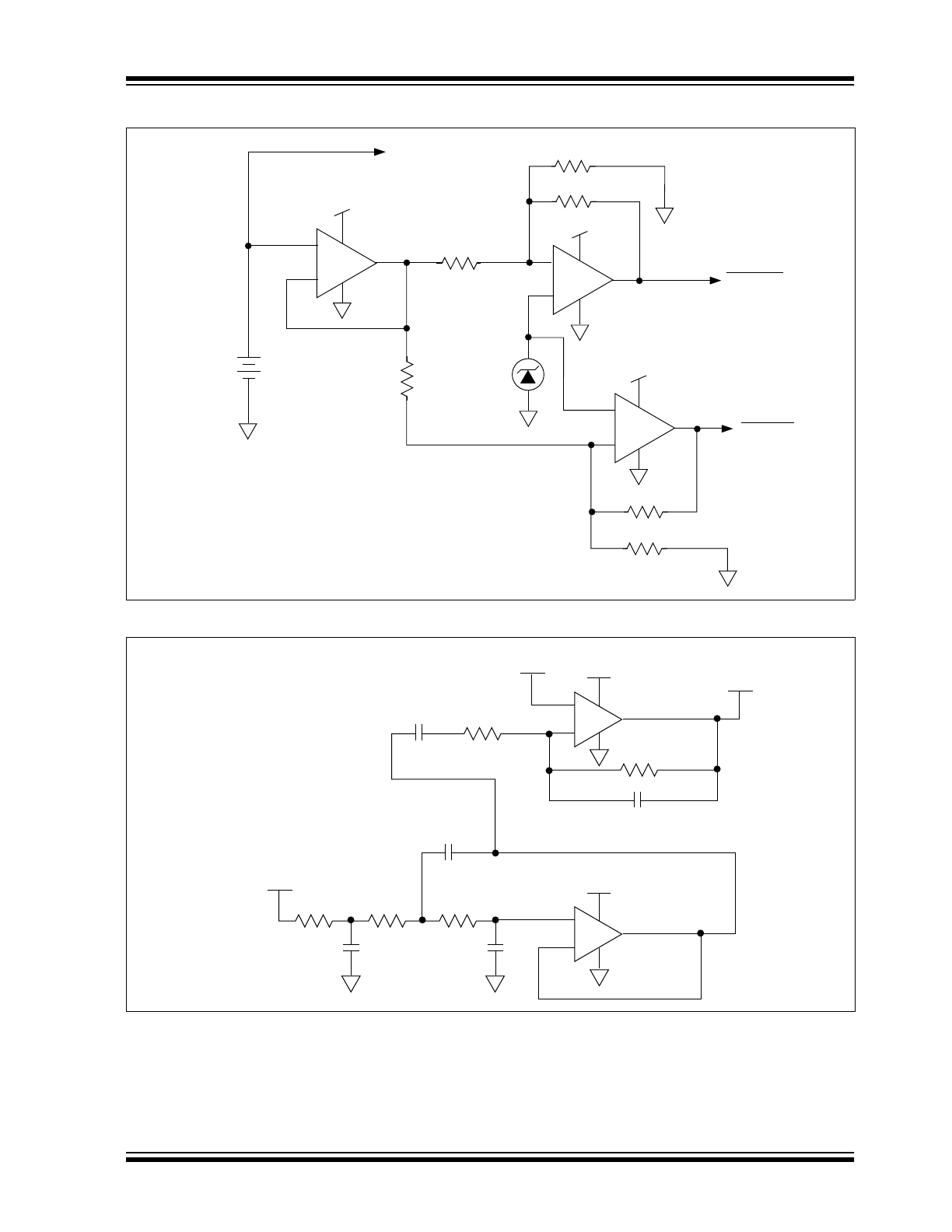
Precision Battery Monitor
Figure 4-2 is a precision battery low/battery dead
monitoring circuit. Typically, the battery low output
warns the user that a battery dead condition is
imminent. Battery dead typically initiates a forced
shutdown to prevent operation at low internal supply
voltages (which can cause unstable system operation).
The circuit of Figure 4-2 uses two TC1026 devices and
only six external resistors. AMP 1 is a simple buffer
while CMPTR1 and CMPTR2 provide precision voltage
detection using V
R
as a reference. Resistors R2 and
R4 set the detection threshold for BATT LOW while
resistors R1and R3 set the detection threshold for
BATT FAIL. The component values shown assert
BATT LOW at 2.2V (typical) and BATT FAIL at 2.0V
(typical). Total current consumed by this circuit is
typically 28
µ
A at 3V. Resistors R5 and R6 provide
hysteresis for comparators CMPTR1 and CMPTR2,
respectively.
4.3
Voice Band Receive Filter
The majority of spectral energy for human voices is in
a 2.7kHz frequency band from 300Hz to 3kHz. To
properly recover a voice signal in applications such as
radios, cellular phones and voice pagers, a low-power
bandpass filter that is matched to the human voice
spectrum can be implemented using Microchip’s
CMOS op amps. Figure 4-3 shows a unity-gain multi-
pole Butterworth filter with ripple less than 0.15dB in
the human voice band. The lower 3dB cut-off frequency
is 70Hz (single-order response), while the upper cut-off
frequency is 3.5kHz (fourth-order response).
4.4
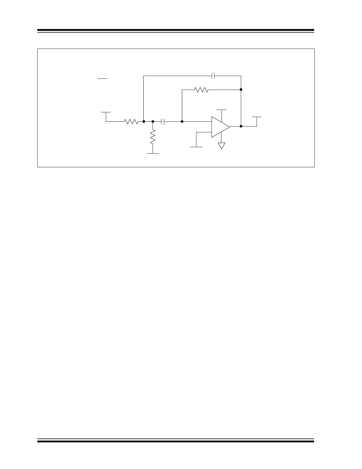
Supervisory Audio Tone (SAT)
Filter for Cellular
Supervisory Audio Tones (SAT) provide a reliable
transmission path between cellular subscriber units
and base stations. The SAT tone functions much like
the current/voltage used in land line telephone systems
to indicate that a phone is off the hook. The SAT tone
may be one of three frequencies: 5970, 6000 or
6030Hz. A loss of SAT implies that channel conditions
are impaired, and if SAT is interrupted for more than 5
seconds, a cellular call is terminated.
Figure 4-4 shows a high Q (30) first order SAT
detection bandpass filter using Microchip’s CMOS op
amp architecture. This circuit nulls all frequencies
except the three SAT tones of interest.
+
–
V
R
V
DD
V
OUT
V
SRC
R
A
R
B
R
C
TC1026
Comparator
TC1026
2002 Microchip Technology Inc.
DS21725B-page 7
TC1026
FIGURE 4-2:
PRECISION BATTERY MONITOR
FIGURE 4-3:
MULTI-POLE BUTTERWORTH VOICE BAND RECEIVE FILTER
V
DD
V
DD
V
DD
R2, 330k, 1%
Op Amp
Comparator
R4, 470k, 1%
R5, 7.5M
Comparator
R6, 7.5M
R3, 470k, 1%
R1, 270k, 1%
VR
To System DC/DC
Converter
3V
Alkaline
TC1026
BATTFAIL
BATTLOW
CMPTR1
+
–
CMPTR2
+
–
AMP1
+
–
+
+
–
+
–
V
OUT
V
IN
21.0k
21.0k
21.0k
2400pF
470pF
750pF
V
DD
V
DD
/2
6800pF
0.1
µF
22.6k
22.6k
Gain = 0dB
Fch = 3.5kHz
-24dB/Octave
Fcl = 70Hz
+6dB/Octave
Passband Ripple
< 0.15dB
Op Amp
TC1026
Op Amp
V
DD
TC1026
DS21725B-page 8
2002 Microchip Technology Inc.
FIGURE 4-4:
SECOND ORDER SAT BANDPASS FILTER
+
–
11.2
24.3k
48.7k
.036
µF
.036
µF
V
IN
V
DD
V
OUT
Gain = 0dB
Q = F
C
BW (3dB)
Q = 30
FC = 6kHz
TC1026
Amp.
V
DD
/2
V
DD
/2
2002 Microchip Technology Inc.
DS21725B-page 9
TC1026
5.0
TYPICAL CHARACTERISTICS
Note:
The graphs and tables provided following this note are a statistical summary based on a limited number of
samples and are provided for informational purposes only. The performance characteristics listed herein
are not tested or guaranteed. In some graphs or tables, the data presented may be outside the specified
operating range (e.g., outside specified power supply range) and therefore outside the warranted range.
7
6
5
4
3
2
1.5
2
2.5
3
3.5
4
4.5
5
5.5
SUPPLY VOLTAGE (V)
SUPPLY VOLTAGE (V)
Comparator Propagation Delay
vs. Supply Voltage
DELAY TO RISING EDGE (
µ
sec)
Overdrive = 10mV
Overdrive = 50mV
7
6
5
4
3
2
1.5
2
2.5
3
3.5
4
4.5
5
5.5
DELAY TO FALLING EDGE (
µ
sec)
7
6
5
4
3
-40
°C
85
°C
25
°C
TEMPERATURE (
°C)
DELAY TO RISING EDGE (
µ
sec)
Overdrive = 100mV
Overdrive = 10mV
Overdrive = 50mV
Comparator Propagation Delay
vs. Supply Voltage
Comparator Propagation Delay
vs. Temperature
T
A
= 25°C
C
L
= 100pF
T
A
= 25°C
C
L
= 100pF
Overdrive = 100mV
V
DD
= 4V
V
DD
= 5V
V
DD
= 2V
V
DD
= 3V
-40
°C
85
°C
25
°C
2.5
2.0
1.5
1.0
.5
0
0
1
2
3
4
5
6
V
DD
- V
OUT
(V)
I
SOURCE
(mA)
7
6
5
4
3
Comparator Output Swing
vs. Output Source Current
DELAY TO FALLING EDGE (
µ
sec)
Overdrive = 100mV
2.5
2.0
1.5
1.0
.5
0
0
1
2
3
4
5
Comparator Propagation Delay
vs. Temperature
Comparator Output Swing
vs. Output Sink Current
TEMPERATURE (
°C)
I
SINK
(mA)
V
DD
= 4V
V
DD
= 5V
V
DD
= 2V
V
DD
= 3V
T
A
= 25°C
T
A
= 25°C
V
DD
= 3V
V
DD
= 1.8V
V
DD
= 5.5V
V
DD
= 3V
V
DD
= 1.8V
V
DD
= 5.5V
V
OUT
- V
SS
(V)
6
60
50
Sinking
40
30
20
10
0
0
1
2
3
4
5
6
OUTPUT SHORT-CIRCUIT CURRENT (mA)
SUPPLY VOLTAGE (V)
Comparator Output Short-Circuit
Current vs. Supply Voltage
Sourcing
T
A
= -40
°C
T
A
= -40
°C
T
A
= 25
°C
T
A
= 85
°C
T
A
= 25
°C
T
A
= 85
°C
REFERENCE VOLTAGE (V)
1.240
1.220
1.200
1.180
1.160
1.140
0
2
4
6
8
10
LOAD CURRENT (mA)
Reference Voltage vs.
Load Current
V
DD
= 1.8V
V
DD
= 3V
V
DD
= 5.5V
Sinking
Sourcing
V
DD
= 1.8V
V
DD
= 3V
V
DD
= 5.5V
4
3
2
1
0
0
100
200
300
400
SUPPLY AND REFERENCE VOLTAGES (V)
TIME (
µsec)
Line Transient
Response of V
REF
V
DD
V
REF
TC1026
DS21725B-page 10
2002 Microchip Technology Inc.
5.0
TYPICAL CHARACTERISTICS (CONTINUED)
Op Amp Short-Circuit Current
vs. Supply Voltage
SUPPLY VOLTAGE (V)
O
UTPUT CURRENT
(mA
)
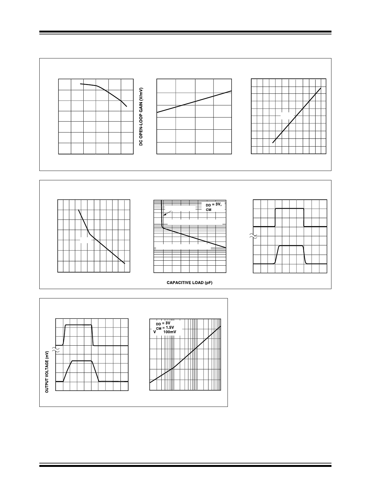
Op Amp DC Open-Loop Gain
vs. Temperature
TEMPERATURE (
°C)
3000
50
45
40
35
30
25
20
15
10
5
0
0.0
1.0
2.0
3.0
4.0
5.0
6.0
2500
2000
1500
1000
500
0
-40
°C
25
°C
85
°C
I
SINK
SUPPLY VOLTAGE (V)
DC OPEN-LOOP GAIN
(dB
)
Op Amp DC Open-Loop Gain
vs. Supply Voltage
140
120
100
80
60
40
20
0
0.0
1.0
2.0
3.0
4.0
5.0
6.0
Op Amp Load Resistance
vs. Load Capacitance
Op Amp Small-Signal
Transient Response
TIME (
µsec)
R
LO
AD
(k
Ω
)
O
UTPUT VOLTAGE
(mV
)
INPUT VOLTAGE
(mV
)
100
50
0
100
50
0
0
250 500 750 1000
10 20 30 40 50 60 70 80
90
12501500 1750 2000
100
10
1
1000
V
V
= 1.5V
10% Overshoot
Region of Marginal Stability
Region of Stable Operation
Op Amp Short-Circuit Current
vs. Supply Voltage
SUPPLY VOLTAGE (V)
O
UTPUT CURRENT
(mA
)
0
-5
-10
-15
-20
-25
-30
-35
0.0
1.0
2.0
3.0
4.0
5.0
6.0
I
SRC
Op Amp Large-Signal
Transient Response
TIME (
µsec)
4
6
2
0
4
6
2
0
10 20 30 40 50 60 70 80
90
INPUT VOLTAGE
(mV
)
Op Amp Power Supply Rejection
Ratio (PSRR) vs. Frequency
FREQUENCY (Hz)
P
SRR
(dB
)
1K
10K
100
0
-10
-20
-30
-40
-50
-60
-70
100K
V
V
IN =
PP