
2002 Microchip Technology Inc.
DS21340B-page 1
Features
• Optimized for Single Supply Operation
• Small Packages: 8-Pin MSOP, 8-Pin PDIP and
8-Pin SOIC
• Ultra Low Input Bias Current: Less than 100pA
• Low Quiescent Current: 12
µ
A (Typ.)
• Rail-to-Rail Inputs and Outputs
• Operates Down to 1.8V
Applications
• Power Management Circuits
• Battery Operated Equipment
• Consumer Products
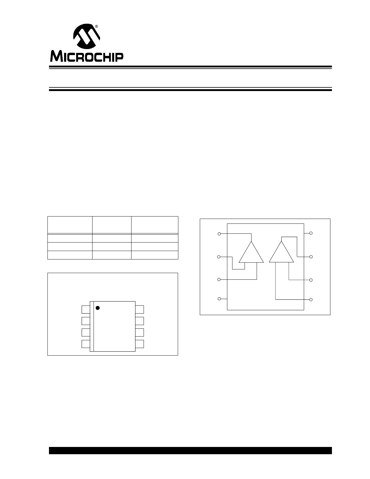
Device Selection Table
Package Types
General Description
The TC1029 is a dual, CMOS operational amplifier
designed for low-power applications. It is designed
specifically for operation from a single supply, however,
operation from dual supplies is also possible, and the
power supply current drain is independent of the
magnitude of the power supply voltage. The TC1029
operates from two 1.5V alkaline cells down to V
DD
=
1.8V. Supply current is only typically 12
µ
A, which
significantly extends battery life.
Rail-to-rail inputs and outputs allow operation from low
supply voltages while accommodating large input
signals, yielding larger output signals.
Packaged in an 8-Pin MSOP, SOIC or DIP, the TC1029
is ideal for battery operated applications.
Functional Block Diagram
Part Number
Package
Temperature
Range
TC1029EPA
8-Pin PDIP
-40°C to +85°C
TC1029EUA
8-Pin MSOP
-40°C to +85°C
TC1029EOA
8-Pin SOIC
-40°C to +85°C
V
SS
V
DD
1
2
3
4
8
7
6
5
TC1029EPA
TC1029EUA
TC1029EOA
8-Pin PDIP
8-Pin MSOP
8-Pin SOIC
OUTB
IN2-
IN2+
IN1+
IN1-
OUTA
+
A
–
+
–
TC1029
OUTB
V
DD
IN2-
IN2+
IN1
-
IN1+
V
SS
OUTA
B
1
2
3
4
8
7
6
5
TC1029
Linear Building Block – Dual Low Power Op Amp
TC1029
DS21340B-page 2
2002 Microchip Technology Inc.
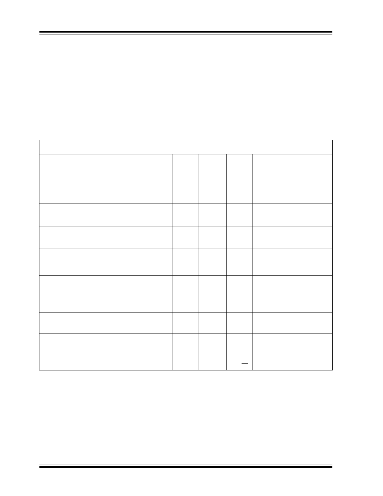
1.0
ELECTRICAL
CHARACTERISTICS
ABSOLUTE MAXIMUM RATINGS*
Supply Voltage ......................................................6.0V
Voltage on Any Pin .......... (V
SS
– 0.5V) to (V
DD
+ 0.5V)
Junction Temperature....................................... +150°C
Operating Temperature Range............. -40°C to +85°C
Storage Temperature Range .............. -55°C to +150°C
*Stresses above those listed under "Absolute Maximum
Ratings" may cause permanent damage to the device. These
are stress ratings only and functional operation of the device
at these or any other conditions above those indicated in the
operation sections of the specifications is not implied.
Exposure to Absolute Maximum Rating conditions for
extended periods may affect device reliability.
TC1029 ELECTRICAL SPECIFICATIONS
Electrical Characteristics: Typical values apply at 25°C and V
DD
= 3.0V; T
A
= -40° to +85°C, and V
DD
= 1.8V to 5.5V, unless
otherwise specified.
Symbol
Parameter
Min
Typ
Max
Units
Test Conditions
V
DD
Supply Voltage
1.8
—
5.5
V
I
Q
Supply Current, Operating
—
12
16
µ
A
All Outputs Open
A
VOL
Large Signal Voltage Gain
—
100
—
V/mV
R
L
= 10k
Ω
, V
DD
= 5V
V
ICMR
Common Mode Input Voltage
Range
V
SS
- 0.2
—
V
DD
+ 0.2
V
V
OS
Input Offset Voltage
±100
±0.3
±500
±1.5
µ
V
mV
V
DD
= 3V, V
CM
= 1.5V, T
A
= 25°C,
T
A
= -40°C to 85°C
I
B
Input Bias Current
-100
50
100
pA
T
A
= 25°C; V
CM
= V
DD
to V
SS
V
OS(DRIFT)
Input Offset Voltage Drift
—
±4
—
µ
V/°C
V
DD
= 3V; V
CM
= 1.5V
GBWP
Gain Bandwidth Product
—
90
—
kHz
V
DD
= 1.8V to 5.5V;
V
O
= V
DD
to V
SS
SR
Slew Rate
—
35
—
mV/
µ
sec
C
L
= 100pF;
R
L
= 1M to GND,
Gain = 1
V
IN
= V
SS
to V
DD
V
OUT
Output Signal Swing
V
SS
+ 0.05
—
V
DD
– 0.05
V
R
L
= 10k
Ω
CMRR
Common Mode Rejection Ratio
70
—
—
dB
T
A
= 25°C; V
DD
= 5V;
V
CM
= V
DD
to V
SS
PSRR
Power Supply Rejection Ratio
80
—
—
dB
T
A
= 25°C; V
CM
= V
SS
;
V
DD
= 1.8V to 5V
I
SRC
Output Source Current
3
—
—
mA
V
IN
= V
DD
Output Shorted to V
SS
V
DD
= 1.8V; Gain = 1
I
SINK
Output Sink Current
4
—
—
mA
V
IN
= V
SS
,
Output Shorted to V
DD
V
DD
= 1.8V; Gain = 1
En
Input Noise Voltage
—
10
—
µ
Vpp
0.1Hz to 10Hz
e
n
Input Noise Voltage Density
—
125
—
nV
/√
HZ
1kHz
2002 Microchip Technology Inc.
DS21340B-page 3
TC1029
2.0
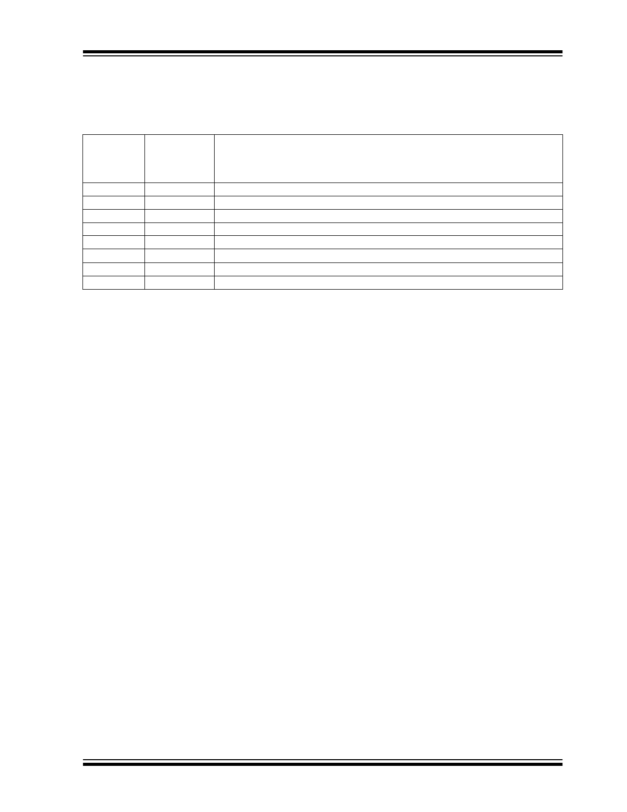
PIN DESCRIPTION
The description of the pins are listed in Table 2-1.
TABLE 2-1:
PIN FUNCTION TABLE
Pin No.
(8-Pin PDIP)
(8-Pin MSOP)
(8-Pin SOIC)
Symbol
Description
1
OUTA
Op amp output.
2
IN1-
Inverting op amp input.
3
IN1+
Non-inverting op amp input.
4
V
SS
Negative power supply.
5
IN2+
Non-inverting op amp input.
6
IN2-
Inverting op amp input.
7
OUTB
Op amp output.
8
V
DD
Positive power supply.

TC1029
DS21340B-page 4
2002 Microchip Technology Inc.
3.0
DETAILED DESCRIPTION
The TC1029 is one of a series of very low power, linear
building block products for low voltage single supply
operations. The TC1029 contains two rail to rail op
amps which operate down to 1.8V with a maximum
supply current of 16
µ
A. The amplifier's input range
extends beyond both supplies by 200mV and the
outputs will swing to within several millivolts of the
supplies, depending on the load current being driven.
The amplifier design is such that large signal gain, slew
rate and bandwidth are largely independent of supply
voltage. The low input bias current and offset voltage of
the TC1029 make it suitable for precision applications.
4.0
TYPICAL APPLICATIONS
The TC1029 lends itself to a wide variety of
applications, particularly in battery powered systems. It
typically finds application in power management,
processor supervisory and interface circuitry.
4.1
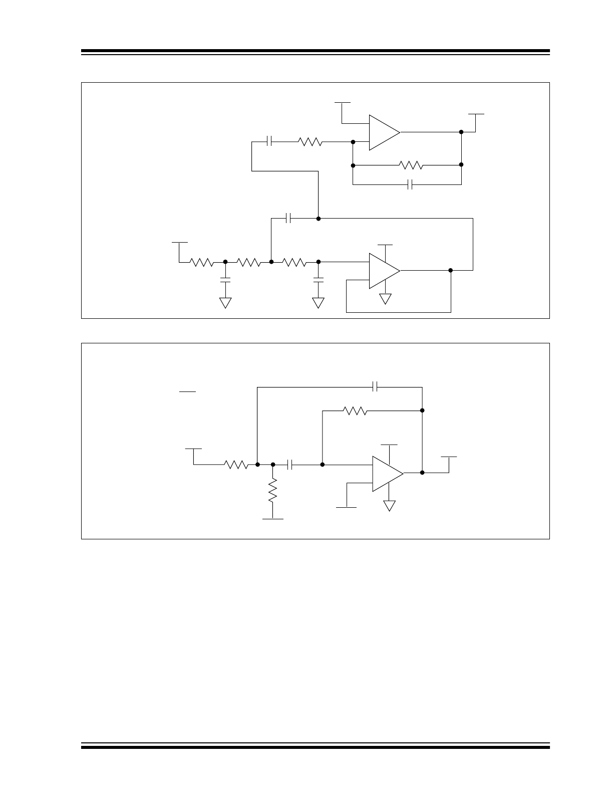
Voice Band Receive Filter
The majority of spectral energy for human voices is
found to be in a 2.7kHz frequency band from 300Hz to
3kHz. To properly recover a voice signal in applications
such as radios, cellular phones and voice pagers, a low
power bandpass filter matched to the human voice
spectrum can be implemented, using Microchip’s
CMOS op amps. Figure 4-1 shows a unity gain multi-
pole Butterworth filter with ripple less than 0.15dB in
the human voice band. The lower 3 dB cut-off
frequency is 70Hz (single order response), while the
upper cut-off frequency is 3.5kHz (fourth order
response).
4.2
Supervisory Audio Tone (SAT)
Filter for Cellular
Supervisory Audio Tones (SAT) provide a reliable
transmission path between cellular subscriber units
and base stations. The SAT tone functions much like
the current/voltage used in land line telephone systems
to indicate that a phone is off the hook. The SAT tone
may be one of three frequencies: 5970, 6000 or
6030Hz. A loss of SAT implies that channel conditions
are impaired and if SAT is interrupted for more than 5
seconds a cellular call is terminated.
Figure 4-2 shows high Q (30) second order SAT
detection bandpass filter using Microchip’s CMOS op
amp architecture. This circuit nulls all frequencies
except the three SAT tones of interest.
2002 Microchip Technology Inc.
DS21340B-page 5
TC1029
FIGURE 4-1:
MULTI-POLE BUTTERWORTH VOICE BAND RECEIVE FILTER
FIGURE 4-2:
SECOND ORDER SAT BANDPASS FILTER
+
–
+
–
V
OUT
V
IN
21.0k
21.0k
21.0k
2400pF
470pF
750pF
V
DD
V
DD
/2
6800pF
0.1
µF
22.6k
22.6k
Gain = 0dB
Fch = 3.5kHz
-24dB/Octave
Fcl = 70Hz
+6dB/Octave
Passband Ripple
< 0.15dB
Op Amp
TC1029
Op Amp
+
–
11.2
24.3k
48.7k
.036
µF
.036
µF
V
IN
V
DD
V
OUT
Gain = 0dB
Q = F
C
BW (3dB)
Q = 30
FC = 6kHz
TC1029
1/2
V
DD
/2
V
DD
/2
TC1029
DS21340B-page 6
2002 Microchip Technology Inc.
5.0
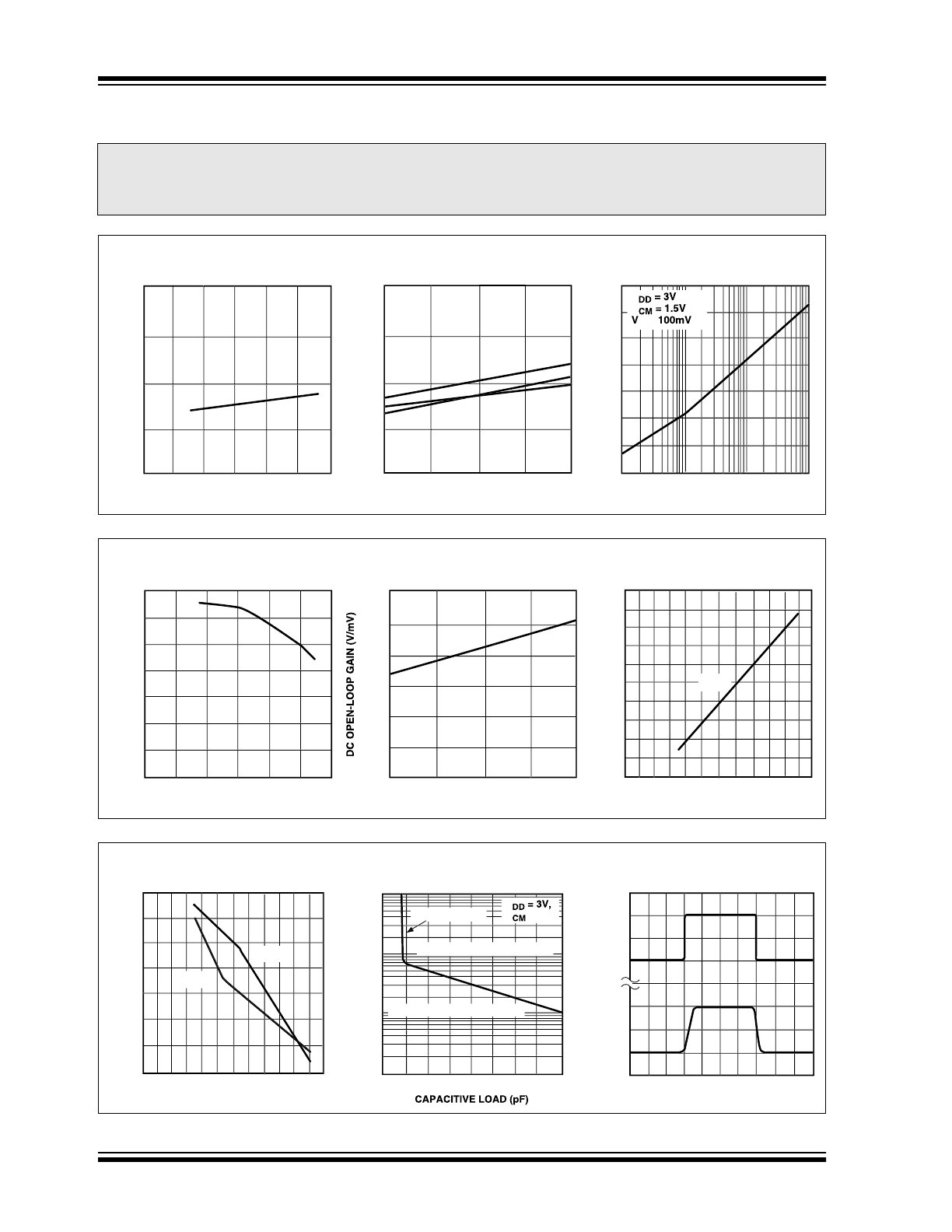
TYPICAL CHARACTERISTICS
Note:
The graphs and tables provided following this note are a statistical summary based on a limited number of
samples and are provided for informational purposes only. The performance characteristics listed herein
are not tested or guaranteed. In some graphs or tables, the data presented may be outside the specified
operating range (e.g., outside specified power supply range) and therefore outside the warranted range.
Op Amp Supply Current
vs. Temperature
Op Amp Supply Voltage
vs. Supply Current
SUPPLY CURRENT (
µ
A
)
SUPPLY VOLTAGE (V)
S
UPPLY CURRENT
(µ
A)
TEMPERATURE (
°C)
Op Amp Power Supply Rejection
Ratio (PSRR) vs. Frequency
FREQUENCY (Hz)
P
SRR
(dB
)
1K
10K
100
0
-10
-20
-30
-40
-50
-60
-70
100K
V
V
IN =
PP
16
12
10
5
0
1
2
3
4
5
6
14
(µ
16
14
12
10
8
-40
°C
25
°C
85
°C
1.8V
3V
5.5V
Op Amp Short-Circuit Current
vs. Supply Voltage
SUPPLY VOLTAGE (V)
O
UTPUT CURRENT
(mA
)
Op Amp DC Open-Loop Gain
vs. Temperature
TEMPERATURE (
°C)
3000
50
45
40
35
30
25
20
15
10
5
0
0.0
1.0
2.0
3.0
4.0
5.0
6.0
2500
2000
1500
1000
500
0
-40
°C
25
°C
85
°C
I
SINK
SUPPLY VOLTAGE (V)
DC OPEN-LOOP GAIN
(dB
)
Op Amp DC Open-Loop Gain
vs. Supply Voltage
140
120
100
80
60
40
20
0
0.0
1.0
2.0
3.0
4.0
5.0
6.0
Op Amp Load Resistance
vs. Load Capacitance
Op Amp Small-Signal
Transient Response
TIME (
µsec)
R
LO
AD
(k
Ω
)
O
UTPUT VOLTAGE
(mV
)
INPUT VOLTAGE
(mV
)
100
50
0
100
50
0
0
250 500 750 1000
10 20 30 40 50 60 70 80
90
12501500 1750 2000
100
10
1
1000
V
V
= 1.5V
10% Overshoot
Region of Marginal Stability
Region of Stable Operation
Op Amp Short-Circuit Current
vs. Supply Voltage
SUPPLY VOLTAGE (V)
O
UTPUT CURRENT
(mA
)
0
-5
-10
-15
-20
-25
-30
-35
0.0
1.0
2.0
3.0
4.0
5.0
6.0
I
SRC-A
I
SRC-B
2002 Microchip Technology Inc.
DS21340B-page 7
TC1029
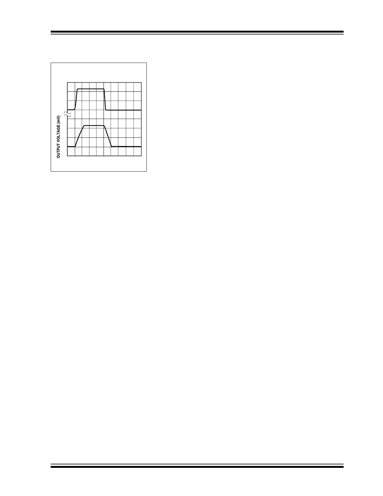
5.0
TYPICAL CHARACTERISTICS (CONTINUED)
Op Amp Large-Signal
Transient Response
TIME (
µsec)
4
6
2
0
4
6
2
0
10 20 30 40 50 60 70 80
90
INPUT VOLTAGE
(mV
)
TC1029
DS21340B-page 8
2002 Microchip Technology Inc.
6.0
PACKAGING INFORMATION
6.1
Package Marking Information
Package marking data not available at this time.
6.2
Taping Form
Component Taping Orientation for 8-Pin MSOP Devices
Package
Carrier Width (W)
Pitch (P)
Part Per Full Reel
Reel Size
8-Pin MSOP
12 mm
8 mm
2500
13 in
Carrier Tape, Number of Components Per Reel and Reel Size
PIN 1
User Direction of Feed
Standard Reel Component Orientation
for TR Suffix Device
W
P
Component Taping Orientation for 8-Pin SOIC (Narrow) Devices
Package
Carrier Width (W)
Pitch (P)
Part Per Full Reel
Reel Size
8-Pin SOIC (N)
12 mm
8 mm
2500
13 in
Carrier Tape, Number of Components Per Reel and Reel Size
Standard Reel Component Orientation
for TR Suffix Device
PIN 1
User Direction of Feed
P
W
2002 Microchip Technology Inc.
DS21340B-page 9
TC1029
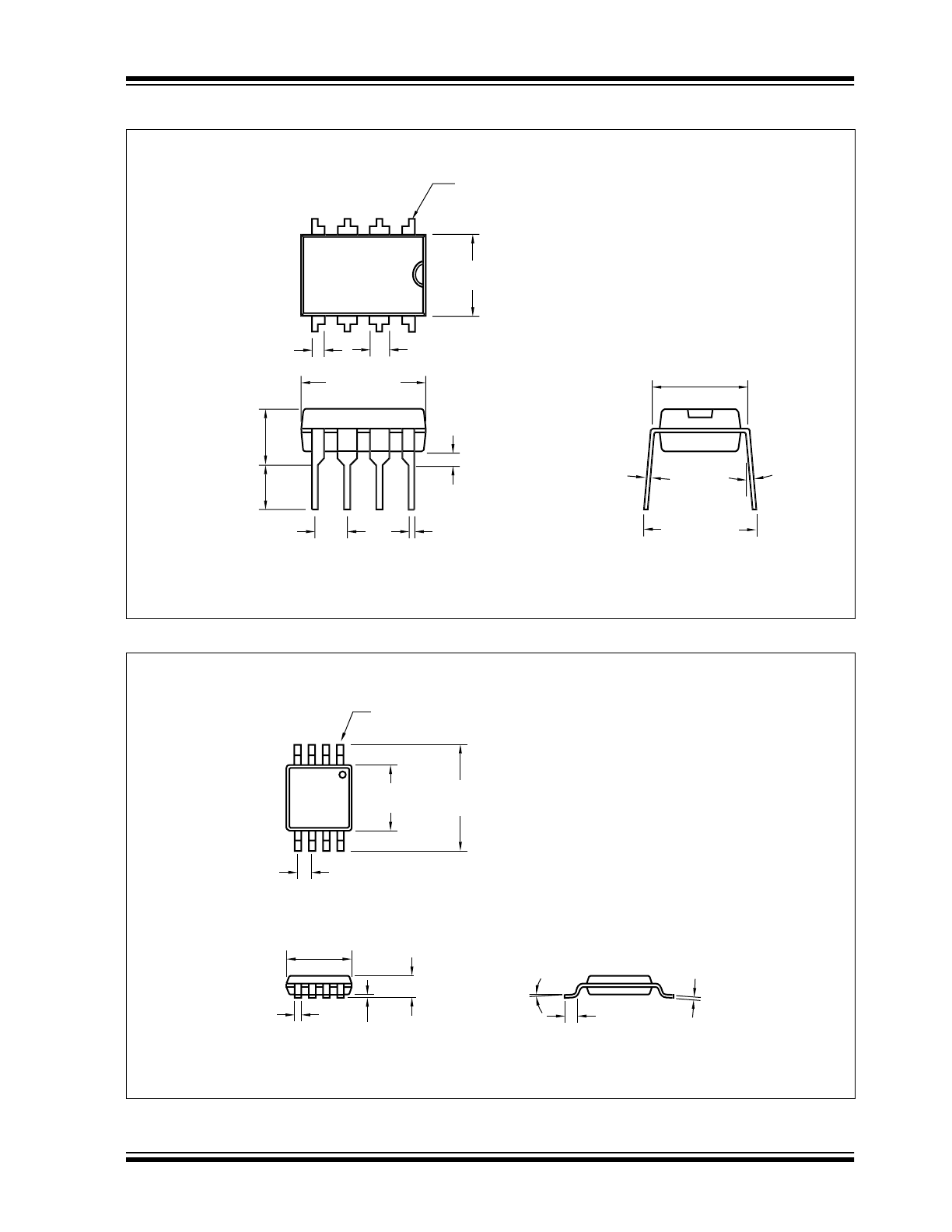
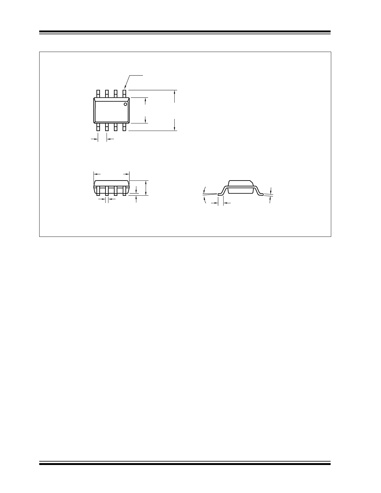
6.3
Package Dimensions
3
° MIN.
PIN 1
.260 (6.60)
.240 (6.10)
.045 (1.14)
.030 (0.76)
.070 (1.78)
.040 (1.02)
.400 (10.16)
.348 (8.84)
.200 (5.08)
.140 (3.56)
.150 (3.81)
.115 (2.92)
.110 (2.79)
.090 (2.29)
.022 (0.56)
.015 (0.38)
.040 (1.02)
.020 (0.51)
.015 (0.38)
.008 (0.20)
.310 (7.87)
.290 (7.37)
.400 (10.16)
.310 (7.87)
8-Pin Plastic DIP
Dimensions: inches (mm)
8-Pin MSOP
.122 (3.10)
.114 (2.90)
.122 (3.10)
.114 (2.90)
.043 (1.10)
MAX.
.006 (0.15)
.002 (0.05)
.016 (0.40)
.010 (0.25)
.197 (5.00)
.189 (4.80)
.008 (0.20)
.005 (0.13)
.028 (0.70)
.016 (0.40)
6
° MAX.
.026 (0.65) TYP.
PIN 1
Dimensions: inches (mm)
TC1029
DS21340B-page 10
2002 Microchip Technology Inc.
6.3
Package Dimensions (Continued)
.050 (1.27) TYP.
8
°
MAX.
PIN 1
.244 (6.20)
.228 (5.79)
.157 (3.99)
.150 (3.81)
.197 (5.00)
.189 (4.80)
.020 (0.51)
.013 (0.33)
.010 (0.25)
.004 (0.10)
.069 (1.75)
.053 (1.35)
.010 (0.25)
.007 (0.18)
.050 (1.27)
.016 (0.40)
.
8-Pin SOIC
Dimensions: inches (mm)