
2002 Microchip Technology Inc.
DS21346B-page 1
Features
• Combines Two Comparators and a Voltage
Reference in a Single Package
• Optimized for Single Supply Operation
• Available in Two Small Packages: 8-Pin SOIC or
8-Pin MSOP
• Ultra Low Input Bias Current: Less than 100pA
• Low Quiescent Current, Operating: 10
µ
A (Typ.)
• Rail-to-Rail Inputs and Outputs
• Operates Down to V
DD
= 1.8V
• Programmable Hysteresis
Applications
• Power Supply Circuits
• Battery Operated Equipment
• Consumer Products
• Replacements for Discrete Components
Device Selection Table
Package Types
General Description
The TC1041 is a mixed-function device combining two
comparators and a voltage reference in a single 8-pin
package. The inverting inputs of both comparators are
internally connected to the reference.
This increased integration allows the user to replace
two packages, which saves space, lowers supply
current and increases system performance. The
TC1041 operates from two 1.5V alkaline cells down to
V
DD
= 1.8V. It requires only 10
µ
A typical supply current
which significantly extends battery life. The TC1041
provides a simple method for adding user-adjustable
hysteresis without feedback or complex external
circuitry. Hysteresis is adjusted with a simple resistor
divider on the HYST pin.
Rail-to-rail inputs and outputs allow operation from low
supply voltages with large input and output signal
swings.
Packaged in an 8-Pin SOIC or 8-Pin MSOP, the
TC1041 is ideal for applications requiring low power
and small packages.
Functional Block Diagram
Part Number
Package
Temperature
Range
TC1041CEOA
8-Pin SOIC
-40°C to +85°C
TC1041CEUA
8-Pin MSOP
-40°C to +85°C
INB-
REF
1
2
3
4
8
7
6
5
TC1041CEOA
TC1041CEUA
8-Pin SOIC
8-Pin MSOP
OUTB
V
DD
INA+
V
SS
OUTA
HYST
+
–
+
–
TC1041
OUTB
V
DD
REF
HYST
INB+
INA+
V
SS
OUTA
B
A
Voltage
Reference
V
SS
1
2
3
4
5
6
7
8
TC1041
Linear Building Block – Dual Low Power Comparator and
Voltage Reference with Programmable Hysteresis
TC1041
DS21346B-page 2
2002 Microchip Technology Inc.
1.0
ELECTRICAL
CHARACTERISTICS
ABSOLUTE MAXIMUM RATINGS*
Supply Voltage ......................................................6.0V
Voltage on Any Pin .......... (V
SS
– 0.3V) to (V
DD
+ 0.3V)
Junction Temperature....................................... +150°C
Operating Temperature Range............. -40°C to +85°C
Storage Temperature Range .............. -55°C to +150°C
*Stresses above those listed under "Absolute Maximum
Ratings" may cause permanent damage to the device. These
are stress ratings only and functional operation of the device
at these or any other conditions above those indicated in the
operation sections of the specifications is not implied.
Exposure to Absolute Maximum Rating conditions for
extended periods may affect device reliability.
TC1041 ELECTRICAL SPECIFICATIONS
Electrical Characteristics: Typical values apply at 25°C and V
DD
= 3.0V. Minimum and maximum values apply for T
A
= -40° to
+85°C and V
DD
= 1.8V to 5.5V, unless otherwise specified.
Symbol
Parameter
Min
Typ
Max
Units
Test Conditions
V
DD
Supply Voltage
1.8
—
5.5
V
I
Q
Supply Current Operating
—
10
15
µ
A
All Outputs Open
Comparators
V
IR
IN+ Voltage Range
V
SS
– 0.2
—
V
DD
+ 0.2
V
V
OS
Input Offset Voltage
-5
-5
—
+5
+5
mV
mV
V
DD
= 3V, T
A
= 25°C
T
A
= -40°C to 85°C (Note 1)
I
B
Input Bias Current
—
—
±100
pA
T
A
= 25°C,
IN+ = V
DD
to V
SS
V
OH
Output High Voltage
V
DD
– 0.3
—
—
V
R
L
= 10k
Ω
to V
SS
V
OL
Output Low Voltage
—
—
0.3
V
R
L
= 10k
Ω
to V
DD
CMRR
Common Mode Rejection Ratio
66
—
—
dB
T
A
= 25°C, V
DD
= 5V
V
CM
= V
DD
to V
SS
PSRR
Power Supply Rejection Ratio
60
—
—
dB
T
A
= 25°C
V
DD
= 1.8V to 5V
I
SRC
Output Source Current
1
—
—
mA
IN+ = V
DD
,
Output Shorted to V
SS
V
DD
= 1.8V
I
SINK
Output Sink Current
2
—
—
mA
IN+ = V
SS
,
Output Shorted to V
DD
V
DD
= 1.8V
V
HYST
Voltage Range at HYST Pin
V
REF
– 0.08
—
V
REF
V
I
HYST
Hysteresis Input Current
—
—
±100
nA
t
PD1
Response Time
—
4
—
µ
sec
100mV Overdrive, C
L
= 100pF
t
PD2
Response Time
—
6
—
µ
sec
10mV Overdrive, C
L
= 100pF
Voltage Reference
V
REF
Reference Voltage
1.176
1.200
1.224
V
I
REF(SOURCE)
Source Current
50
—
—
µ
A
I
REF(SINK)
Sink Current
50
—
—
µ
A
C
L(REF)
Load Capacitance
—
—
100
pF
E
VREF
Noise Voltage
—
20
—
µ
V
RMS
100Hz to 100kHz
e
VREF
Noise Voltage Density
—
1.0
—
µ
V/
√
Hz
1kHz
Note
1:
V
OS
is measured as (V
UT
+ V
LT
– 2V
REF
)/2 where V
UT
is the upper hysteresis threshold and V
LT
is the lower hysteresis threshold with
V
REF
– V
HYST
set to 10mV. This represents the assymetry of the hysteresis thresholds around V
REF
.
2002 Microchip Technology Inc.
DS21346B-page 3
TC1041
2.0
PIN DESCRIPTION
The description of the pins are listed in Table 2-1.
TABLE 2-1:
PIN FUNCTION TABLE
Pin No.
(8-Pin SOIC)
(8-Pin MSOP)
Symbol
Description
1
OUTA
Comparator output.
2
V
SS
Negative power supply.
3
INA+
Non-inverting input to Comparator A.
4
INB-
Non-Inverting input to Comparator B.
5
HYST
Adjustable hysteresis input.
6
REF
Voltage reference output.
7
V
DD
Positive power supply.
8
OUTB
Comparator output.
TC1041
DS21346B-page 4
2002 Microchip Technology Inc.
3.0
DETAILED DESCRIPTION
The TC1041 is one of a series of very low power, linear
building block products targeted at low voltage
operation. The TC1041 contains two comparators and
a voltage reference and operates at a minimum supply
voltage of 1.8V with a typical current consumption of
10
µ
A.
Both
comparators
have
programmable
hysteresis.
3.1
Comparator
The TC1041 contains two comparators with program-
mable
hysteresis.
The
inverting
inputs
of
the
comparators are connected to the output of the voltage
reference, while the range of the non-inverting inputs
extend beyond both supply voltages by 200mV. The
comparator outputs will swing to within several
millivolts of the supplies depending on the load current
being driven.
The comparators exhibit a propagation delay and
supply current which are largely independent of supply
voltage. The low input bias current and offset voltage
make them suitable for high impedance precision
applications.
3.2
Voltage Reference
A 2.0 percent tolerance, internally biased, 1.20V band-
gap voltage reference is included in the TC1041. It has
a push-pull output capable of sourcing and sinking at
least 50
µ
A.
3.3
Programmable Hysteresis
Hysteresis is added to the comparators by connecting
a resistor, R1, between the V
REF
and HYST pins and
another resistor, R2, between the HYST pin and V
SS
.
For no hysteresis, V
REF
should be directly connected to
HYST. The hysteresis, V
HB
, is equal to twice the
voltage difference between the V
REF
and HYST pins
where:
and is symmetrical around the normal (without
hysterersis)
threshold
of
the
comparator.
The
maximum voltage allowed between the V
REF
and H
YST
pins is 80mV, giving a maximum hysteresis of 160mV.
FIGURE 3-1:
TC1041 PROGRAMMABLE HYSTERESIS
V
HB
= 2V
REF
R1/(R1 + R2) (See Figure 3-1)
V
REF
HYST
V
SS
TC1041
6
5
1
R1
R2
I
REF
R1 =
V
HB
(2) (I
REF
)
R2 =
I
REF
(
1.2V –
)
V
HB
2
Note: Size R1 and R2 such that I
REF
≤ 50µA
2002 Microchip Technology Inc.
DS21346B-page 5
TC1041
4.0
TYPICAL APPLICATIONS
The TC1041 lends itself to a wide variety of
applications, particularly in battery powered systems. It
typically finds application in power management,
processor supervisory and interface circuitry.
4.1
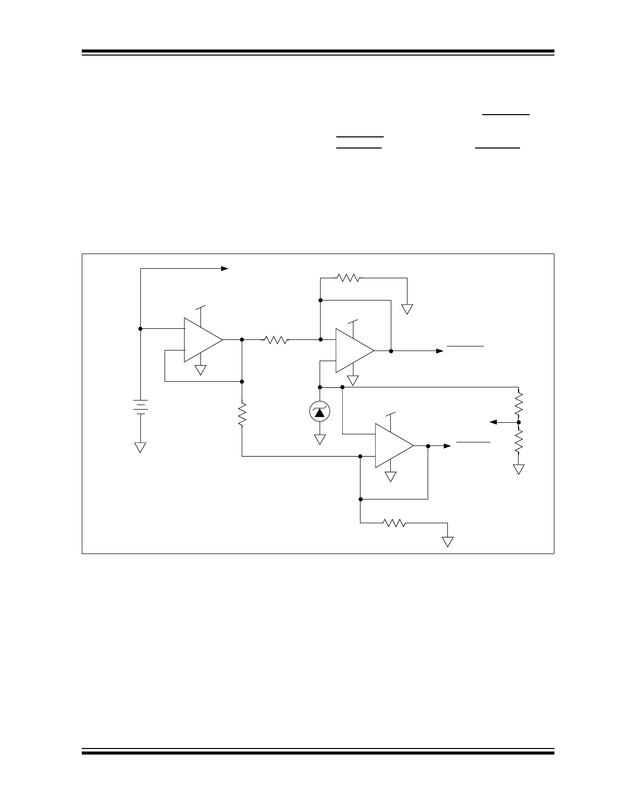
Precision Battery Monitor
Figure 4-1 is a precision battery low/battery dead
monitoring circuit. Typically, the battery low output
warns the user that a battery dead condition is
imminent. Battery dead typically initiates a forced
shutdown to prevent operation at low internal supply
voltages (which can cause unstable system operation).
The circuit in Figure 4-1 uses a TC1034, a TC1041 and
only six external resistors. AMP 1 is a simple buffer
while CMPTR1 and CMPTR2 provide precision voltage
detection using V
REF
as a reference. Resistors R2 and
R4 set the detection threshold for BATT LOW while
Resistors R1 and R3 set the detection threshold for
BATT FAIL. The component values shown assert
BATT LOW at 2.2V (typical) and BATT FAIL at 2.0V
(typical). Total current consumed by this circuit is
typically 16
µ
A at 3V. Resistors R5 and R6 provide
hysteresis of 116mV for both comparators.
FIGURE 4-1:
PRECISION BATTERY MONITOR
V
DD
V
DD
V
DD
R2, 430k, 1%
R4, 470k, 1%
R3, 470k, 1%
R1, 300k, 1%
V
REF
To System DC/DC
Converter
3V
Alkaline
TC1041
BATTFAIL
BATTLOW
CMPTR1
+
–
CMPTR2
+
–
AMP1
+
–
+
TC1034
TC1041
TC1041
HYST
51k
R6
R5
1M
TC1041
DS21346B-page 6
2002 Microchip Technology Inc.
5.0
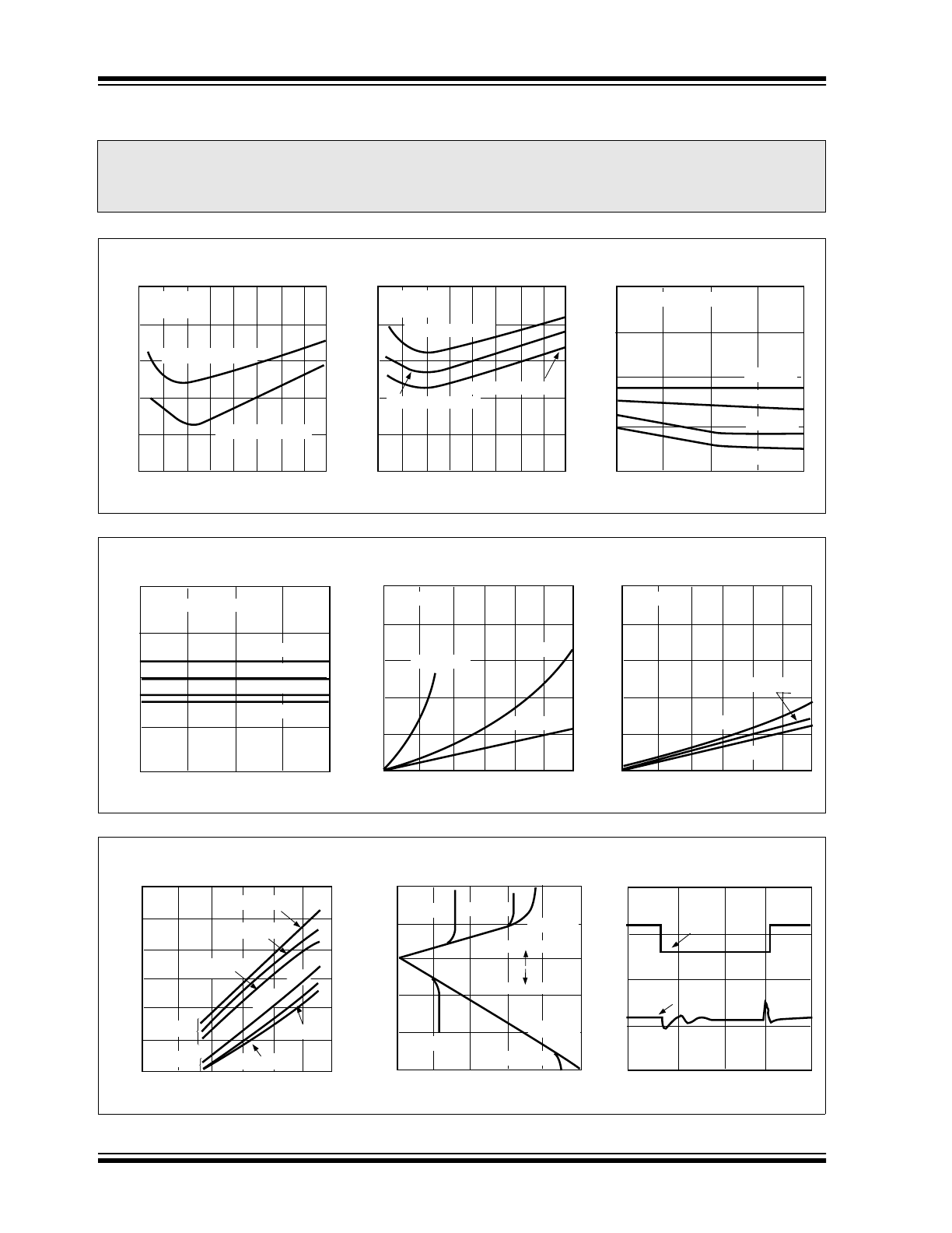
TYPICAL CHARACTERISTICS
Note:
The graphs and tables provided following this note are a statistical summary based on a limited number of
samples and are provided for informational purposes only. The performance characteristics listed herein
are not tested or guaranteed. In some graphs or tables, the data presented may be outside the specified
operating range (e.g., outside specified power supply range) and therefore outside the warranted range.
7
6
5
4
3
2
1.5
2
2.5
3
3.5
4
4.5
5
5.5
SUPPLY VOLTAGE (V)
SUPPLY VOLTAGE (V)
Comparator Propagation Delay
vs. Supply Voltage
DELAY TO RISING EDGE (
µ
sec)
Overdrive = 10mV
Overdrive = 50mV
7
6
5
4
3
2
1.5
2
2.5
3
3.5
4
4.5
5
5.5
DELAY TO FALLING EDGE (
µ
sec)
7
6
5
4
3
-40
°C
85
°C
25
°C
TEMPERATURE (
°C)
DELAY TO RISING EDGE (
µ
sec)
Overdrive = 100mV
Overdrive = 10mV
Overdrive = 50mV
Comparator Propagation Delay
vs. Supply Voltage
Comparator Propagation Delay
vs. Temperature
T
A
= 25°C
C
L
= 100pF
T
A
= 25°C
C
L
= 100pF
Overdrive = 100mV
V
DD
= 4V
V
DD
= 5V
V
DD
= 2V
V
DD
= 3V
-40
°C
85
°C
25
°C
2.5
2.0
1.5
1.0
.5
0
0
1
2
3
4
5
6
V
DD
- V
OUT
(V)
I
SOURCE
(mA)
7
6
5
4
3
Comparator Output Swing
vs. Output Source Current
DELAY TO FALLING EDGE (
µ
sec)
Overdrive = 100mV
2.5
2.0
1.5
1.0
.5
0
0
1
2
3
4
5
Comparator Propagation Delay
vs. Temperature
Comparator Output Swing
vs. Output Sink Current
TEMPERATURE (
°C)
I
SINK
(mA)
V
DD
= 4V
V
DD
= 5V
V
DD
= 2V
V
DD
= 3V
T
A
= 25°C
T
A
= 25°C
V
DD
= 3V
V
DD
= 1.8V
V
DD
= 5.5V
V
DD
= 3V
V
DD
= 1.8V
V
DD
= 5.5V
V
OUT
- V
SS
(V)
6
60
50
Sinking
40
30
20
10
0
0
1
2
3
4
5
6
OUTPUT SHORT-CIRCUIT CURRENT (mA)
SUPPLY VOLTAGE (V)
Comparator Output Short-Circuit
Current vs. Supply Voltage
Sourcing
T
A
= -40
°C
T
A
= -40
°C
T
A
= 25
°C
T
A
= 85
°C
T
A
= 25
°C
T
A
= 85
°C
REFERENCE VOLTAGE (V)
1.240
1.220
1.200
1.180
1.160
1.140
0
2
4
6
8
10
LOAD CURRENT (mA)
Reference Voltage vs.
Load Current
V
DD
= 1.8V
V
DD
= 3V
V
DD
= 5.5V
Sinking
Sourcing
V
DD
= 1.8V
V
DD
= 3V
V
DD
= 5.5V
4
3
2
1
0
0
100
200
300
400
SUPPLY AND REFERENCE VOLTAGES (V)
TIME (
µsec)
Line Transient
Response of V
REF
V
DD
V
REF
2002 Microchip Technology Inc.
DS21346B-page 7
TC1041
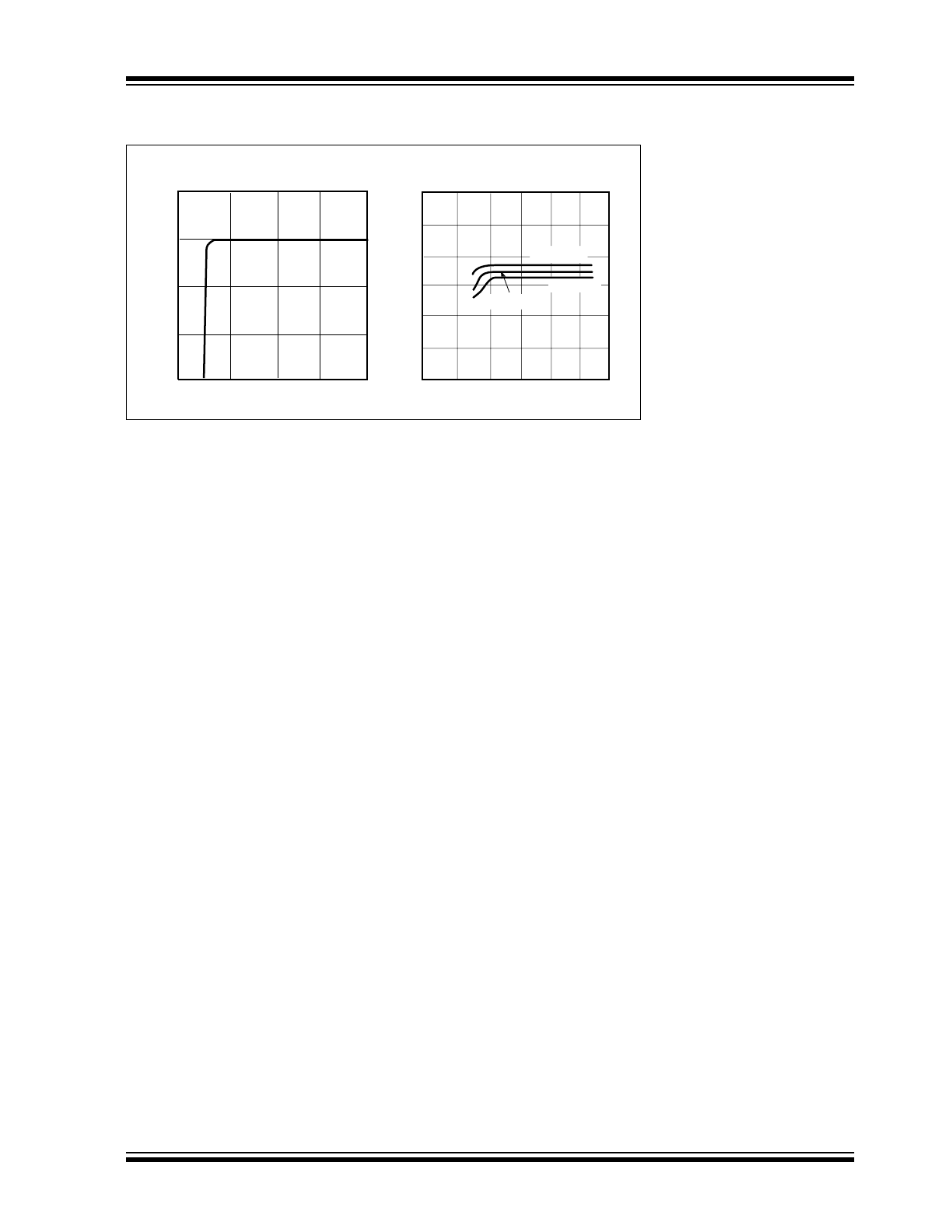
5.0
TYPICAL CHARACTERISTICS (CONTINUED)
1.25
1.20
1.15
1.10
1.05
1
2
3
4
5
REFERENCE VOLTAGE (V)
0
1
2
3
4
5
6
SUPPLY CURRENT
(µ
A)
SUPPLY VOLTAGE (V)
Supply Current vs. Supply Voltage
T
A
= 85
°
C
T
A
= -40
°
C
T
A
= 25
°
C
Reference Voltage
vs. Supply Voltage
SUPPLY VOLTAGE (V)
12
11
10
9
8
7
6
TC1041
DS21346B-page 8
2002 Microchip Technology Inc.
6.0
PACKAGING INFORMATION
6.1
Package Marking Information
Package marking data not available at this time.
6.2
Taping Form
Component Taping Orientation for 8-Pin MSOP Devices
Package
Carrier Width (W)
Pitch (P)
Part Per Full Reel
Reel Size
8-Pin MSOP
12 mm
8 mm
2500
13 in
Carrier Tape, Number of Components Per Reel and Reel Size
PIN 1
User Direction of Feed
Standard Reel Component Orientation
for TR Suffix Device
W
P
Component Taping Orientation for 8-Pin SOIC (Narrow) Devices
Package
Carrier Width (W)
Pitch (P)
Part Per Full Reel
Reel Size
8-Pin SOIC (N)
12 mm
8 mm
2500
13 in
Carrier Tape, Number of Components Per Reel and Reel Size
Standard Reel Component Orientation
for TR Suffix Device
PIN 1
User Direction of Feed
P
W
2002 Microchip Technology Inc.
DS21346B-page 9
TC1041
6.3
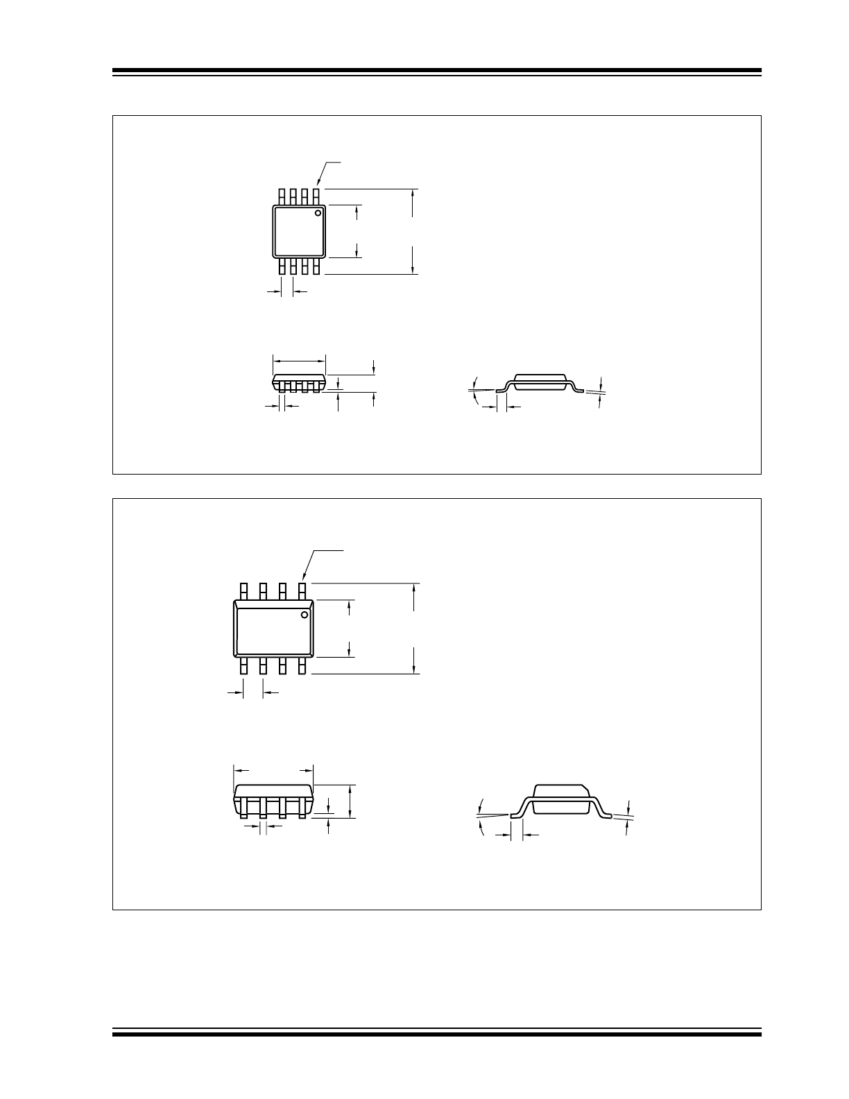
Package Dimensions
8-Pin MSOP
.122 (3.10)
.114 (2.90)
.122 (3.10)
.114 (2.90)
.043 (1.10)
MAX.
.006 (0.15)
.002 (0.05)
.016 (0.40)
.010 (0.25)
.197 (5.00)
.189 (4.80)
.008 (0.20)
.005 (0.13)
.028 (0.70)
.016 (0.40)
6
° MAX.
.026 (0.65) TYP.
PIN 1
Dimensions: inches (mm)
.050 (1.27) TYP.
8
°
MAX.
PIN 1
.244 (6.20)
.228 (5.79)
.157 (3.99)
.150 (3.81)
.197 (5.00)
.189 (4.80)
.020 (0.51)
.013 (0.33)
.010 (0.25)
.004 (0.10)
.069 (1.75)
.053 (1.35)
.010 (0.25)
.007 (0.18)
.050 (1.27)
.016 (0.40)
.
8-Pin SOIC
Dimensions: inches (mm)

TC1041
DS21346B-page 10
2002 Microchip Technology Inc.
NOTES: