

2005-2014 Microchip Technology Inc.
DS20002018H-page 1
MCP2021/2/1P/2P
Features:
• The MCP2021/2/1P/2P are Compliant with LIN
Bus Specifications 1.3, 2.1 and are Compliant to
SAE J2602-2
• Support Baud Rates up to 20 kBaud
with
LIN-compatible Output Driver
• 43V Load Dump Protected
• Very Low EMI Meets Stringent OEM Requirements
• Wide Supply Voltage, 6.0V-18.0V Continuous:
- Maximum input voltage of 30V
• Extended Temperature Range: -40 to +125°C
• Interface to PIC
®
EUSART and Standard USARTs
• Local Interconnect Network (LIN) Bus Pin:
- Internal pull-up resistor and diode
- Protected against ground shorts
- Protected against loss of ground
- High-current drive
• Automatic Thermal Shutdown
• On-Chip Voltage Regulator:
- Output voltage of 5.0V with tolerances of
±3% overtemperature range
- Available with alternate output voltage of
3.3V with tolerances of ±3% overtemperature
range
- Maximum continuous input voltage of 30V
- Internal thermal overload protection
- Internal short circuit current limit
- External components limited to filter capacitor
and load capacitor
• Two Low-Power modes:
- Receiver On, Transmitter Off, Voltage
Regulator On (
85 µA)
- Receiver Monitoring Bus, Transmitter Off,
Voltage Regulator Off (
16 µA)
Description:
The MCP2021/2/1P/2P provides a bidirectional, half-
duplex communication physical interface to automotive
and industrial LIN systems that meets the LIN bus
specification Revision 2.1 and SAE J2602-2. The
devices incorporate a voltage regulator with 5V at
50 mA or 3.3V at 50 mA regulated power-supply
outputs.
The regulator is short-circuit protected, and is protected
by an internal thermal shutdown circuit. The device has
been specifically designed to operate in the automotive
operating environment and will survive all specified
transient conditions while meeting all of the stringent
quiescent current requirements.
The MCP2021/2/1P/2P family of devices includes the
following packages.
8-pin PDIP, DFN and SOIC packages:
• MCP2021-330, LIN-compatible driver, 8-pin, 3.3V
regulator, wake up on dominant level of L
BUS
• MCP2021-500, LIN-compatible driver, 8-pin, 5.0V
regulator, wake up on dominant level of L
BUS
• MCP2021P-330, LIN-compatible driver, 8-pin,
3.3V regulator, wake up at falling edge of L
BUS
voltage
• MCP2021P-500, LIN-compatible driver, 8-pin,
5.0V regulator, wake up at falling edge of L
BUS
voltage
14-pin PDIP, TSSOP and SOIC packages with RESET
output:
• MCP2022-330, LIN-compatible driver, 14-pin,
3.3V regulator, RESET output, wake up on
dominant level of L
BUS
• MCP2022-500, LIN-compatible driver, 14-pin,
5.0V regulator, RESET output, wake up on
dominant level of L
BUS
• MCP2022P-330, LIN-compatible driver, 14-pin,
3.3V regulator, RESET output, wake up at falling
edge of LBUS voltage
• MCP2022P-500, LIN-compatible driver, 14-pin,
5.0V regulator, RESET output, wake up at falling
edge of L
BUS
voltage
LIN Transceiver with Voltage Regulator
MCP2021/2/1P/2P
DS20002018H-page 2
2005-2014 Microchip Technology Inc.
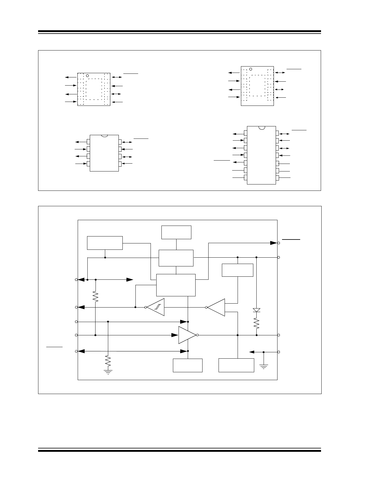
Package Types
MCP2021/2 Block Diagram
1
2
3
4
8
7
6
5
1
2
3
4
14
13
12
11
10
9
8
5
6
7
R
XD
CS/LWAKE
V
REG
T
XD
FAULT/T
XE
V
BB
L
BUS
V
SS
R
XD
CS/LWAKE
V
REG
T
XD
RESET
NC
NC
FAULT/T
XE
V
BB
L
BUS
V
SS
NC
NC
NC
MCP2021, MCP2021P
4x4 DFN*
1
2
3
4
8
7
6
5
EP
9
MCP2021, MCP2021P
PDIP, SOIC
MCP2022, MCP2022P
PDIP, SOIC, TSSOP
R
XD
CS/LWAKE
V
REG
T
XD
FAULT/T
XE
V
BB
L
BUS
V
SS
* Includes Exposed Thermal Pad (EP); see
Table 1-2
.
1
2
3
4
8
7
6
5
EP
9
R
XD
CS/LWAKE
V
REG
T
XD
FAULT/T
XE
V
BB
L
BUS
V
SS
MCP2021,
6x5 DFN-S*
Voltage
Regulator
Ratiometric
Reference
OC
Thermal
Protection
Internal Circuits
V
REG
FAULT/T
XE
R
XD
T
XD
V
BB
L
BUS
V
SS
~30 kΩ
CS/LWAKE
Wake-Up
Logic and
Power Control
RESET
Short Circuit
Protection
Short Circuit
Protection
Thermal
Protection
(MCP2022
ONLY
)
–
+
2005-2014 Microchip Technology Inc.
DS20002018H-page 3
MCP2021/2/1P/2P
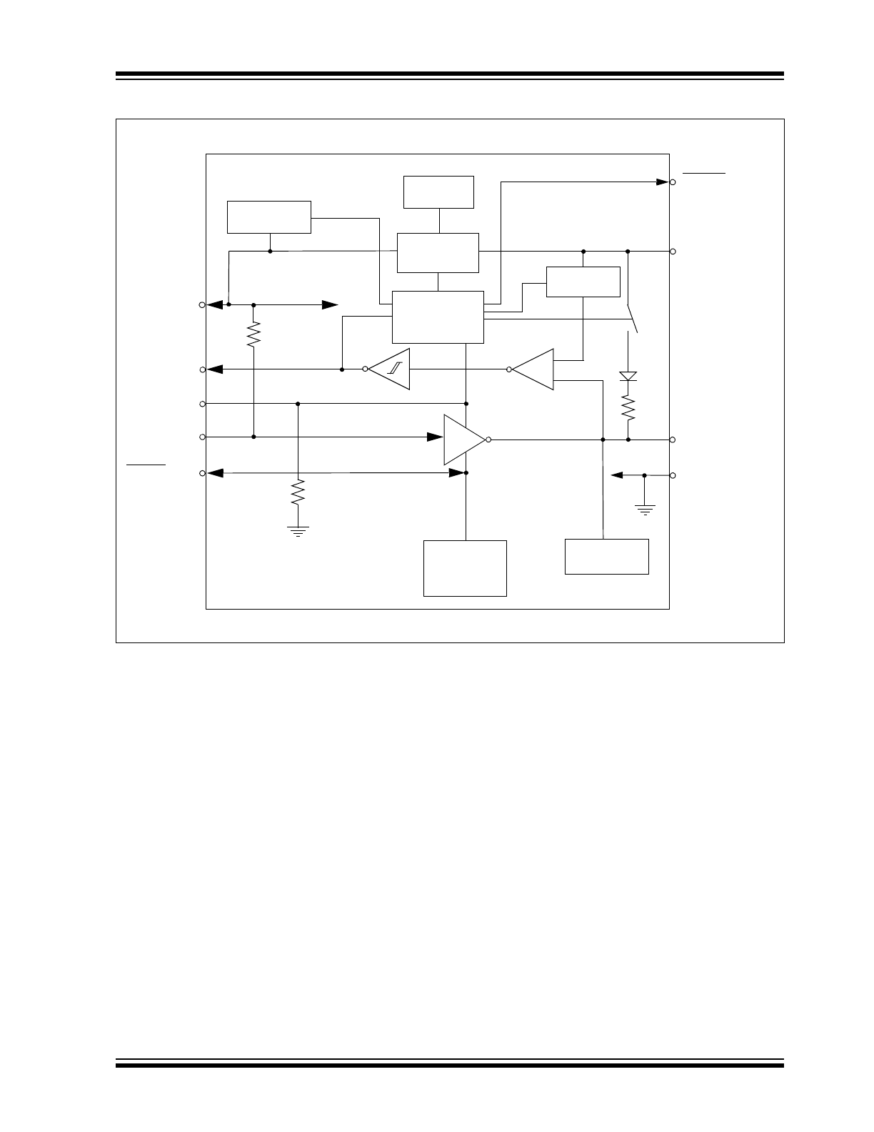
MCP2021P/2P Block Diagram
Ratiometric
Reference
Internal Circuits
V
REG
R
XD
T
XD
V
BB
V
SS
~30
Wake-Up
Logic and
Power Control
RESET
Thermal
Protection
kΩ
(MCP2022P
ONLY
)
L
BUS
Short-Circuit
Protection
OC
CS/LWAKE
FAULT/T
XE
–
+
Voltage
Regulator
Short-Circuit
Protection
Thermal
Short-Circuit
Protection
and

MCP2021/2/1P/2P
DS20002018H-page 4
2005-2014 Microchip Technology Inc.
NOTES:

2005-2014 Microchip Technology Inc.
DS20002018H-page 5
MCP2021/2/1P/2P
1.0
DEVICE OVERVIEW
The MCP2021/2/1P/2P provides a physical interface
between a microcontroller and a LIN half-duplex bus. It
is intended for automotive and industrial applications
with serial bus speeds up to 20 Kbaud.
The MCP2021/2/1P/2P provides a half-duplex,
bidirectional communications interface between a
microcontroller and the serial network bus. This device
will translate the CMOS/TTL logic levels to LIN-level
logic, and vice versa.
The LIN specification 2.0 requires that the
transceiver(s) of all nodes in the system be connected
via the LIN pin, referenced to ground, and with a
maximum external termination resistance load of 510Ω
from LIN bus to battery supply. The 510Ω
corresponds
to one Master and sixteen Slave nodes.
The MCP2021/2/1P/2P-500 provides a +5V, 50 mA,
regulated power output. The regulator uses an LDO
design, is short-circuit protected, and will turn the
regulator output off if it falls below 3.5V.
The MCP2021/2/1P/2P also includes
thermal-shutdown protection.
The regulator is specifically designed to operate in the
automotive environment and will survive +43V load
dump transients, double-battery jumps, and reverse
battery connections when a reverse blocking diode is
used. The other members of the
MCP2021/2/1P/2P-330 family output +3.3V at 50 mA
with a turn-off voltage of 2.5V. (See
Section 1.6
“Internal Voltage Regulator”
).
MCP2021/2 wakes from Power-Down mode on a
dominant level on L
BUS
. MCP2021P/2P wakes at a
transition from recessive level to dominant level on
LBUS.
1.1
Optional External Protection
1.1.1
REVERSE BATTERY PROTECTION
An external reverse-battery-blocking diode should be
used to provide polarity protection (see
Figure 1-6
).
1.1.2
TRANSIENT VOLTAGE
PROTECTION (LOAD DUMP)
An external 43V transient suppressor (TVS) diode,
between V
BB
and ground, with a 50Ω transient protec-
tion resistor (R
TP
) in series with the battery supply and
the V
BB
pin, protect the device from power transients
(see
Figure 1-6
) and ESD events. While this protection
is optional, it is considered good engineering practice.
The resistor value is chosen according to
Equation 1-1
.
EQUATION 1-1:
1.2
Internal Protection
1.2.1
ESD PROTECTION
For component-level ESD ratings, please refer to the
Section 2.1 “Absolute Maximum Ratings†”
.
1.2.2
GROUND LOSS PROTECTION
The LIN Bus specification states that the LIN pin must
transition to the recessive state when ground is
disconnected. Therefore, a loss of ground effectively
forces the LIN line to a high-impedance level.
1.2.3
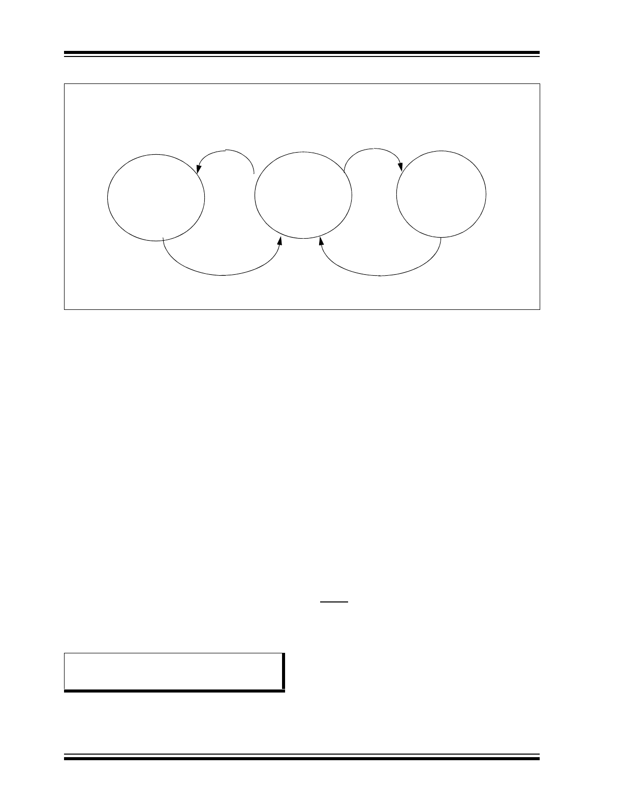
THERMAL PROTECTION
The thermal protection circuit monitors the die tem-
perature and is able to shut down the
LIN transmitter
and voltage regulator if it detects a thermal overload.
There are three causes for a thermal overload. A
thermal shut down can be triggered by any one, or a
combination of, the following thermal overload
conditions:
• Voltage regulator overload
• LIN bus output overload
• Increase in die temperature due to increase in
environmental temperature
Driving the T
XD
and checking the R
XD
pin makes it pos-
sible to determine whether there is a bus contention
(i.e., R
XD
= low, T
XD
= high) or a thermal overload con-
dition (i.e., R
XD
= high, T
XD
= low).
R
TP
(V
BBmin
- 5.5) / 250 mA.
5.5V = V
UVLO
+ 1.0V,
250 mA is the peak current at Power-On when
V
BB
= 5.5V
MCP2021/2/1P/2P
DS20002018H-page 6
2005-2014 Microchip Technology Inc.
FIGURE 1-1:
THERMAL SHUTDOWN STATE DIAGRAMS
1.3
Modes of Operation
For an overview of all operational modes, please refer
to
Table 1-1
.
1.3.1
POWER-ON RESET MODE
Upon application of V
BB
, the device enters Power-On
Reset mode (POR). During this mode, the part main-
tains the digital section in a Reset mode and waits until
the voltage on pin V
BB
rises above the “ON” threshold
(typically 5.75V) to enter to the Ready mode. If during
the operation, the voltage on pin V
BB
falls below the
“OFF” threshold (typically 4.25V), the part comes back
to the POR mode.
1.3.2
POWER-DOWN MODE
In Power-Down mode, the transmitter and the voltage
regulator are off. Only the receiver wake-up from the
LIN bus section, and the CS/LWAKE pin wake-up
circuits, are in operation. This is the lowest power
mode.
If pin CS/LWAKE goes to a high level during
Power-Down mode, the device immediately enters
Ready mode and enables the voltage regulator; and
after the output has stabilized (approximately 0.3 ms to
1.2 ms), the device goes to Operation mode or Trans-
mitter-Off mode (see
Figure 1-2
for MCP2021/2 and
Figure 1-4
for MCP2021P/2P).
LIN bus activity will also change the device from
Power-Down mode to Ready mode. MCP2021/2
wakes up on the dominant level of the LIN bus, and
MCP2021P/2P on a falling edge that follows a domi-
nant level lasting 20 µs of time.
The Power-Down mode can be reached through either
Operation mode or Transmitter-Off mode.
1.3.3
READY MODE
Upon entering Ready mode, the voltage regulator and
receiver-threshold-detect circuit are powered up. The
transmitter remains in an OFF state. The device is
ready to receive data as soon as the regulator is stabi-
lized, but not to transmit. If a microcontroller is being
driven by the voltage regulator output, it will go through
a POR and initialization sequence. The LIN pin is in the
recessive state for MCP2021/2 and in floating state for
MCP2021P/2P.
The device will stay in Ready mode until the output of
the voltage regulator has stabilized and the CS/LWAKE
pin is true (‘1’). After V
REG
is stable and CS/LWAKE is
high, MCP2021/2 will enter Operation mode; and
MCP2021P/2P will enter either Operation mode or
Transmitter-Off mode, depending on the level of the
FAULT/T
XE
pin (refer to
Figure 1-4
).
1.3.4
OPERATION MODE
In this mode, all internal modules are operational.
The device will go into the Power-Down mode on the
falling edge of CS/LWAKE.
For the MCP2021P/2P devices, the pull-up resistor is
switched on only in this mode.
Operation
Mode
Transmitter
Shutdown
L
BUS
Voltage
Shutdown
Regulator
Output
Temperature <SHUTDOWN
TEMP
Overload
to V
BB
Overload
Temperature <SHUTDOWN
TEMP
Note:
The above time interval <1.2 ms assumes
12V V
BB
input and no thermal shutdown
event.

2005-2014 Microchip Technology Inc.
DS20002018H-page 7
MCP2021/2/1P/2P
1.3.5
TRANSMITTER-OFF MODE
Whenever the FAULT/T
XE
signal is low, or permanent
dominant on T
XD
/L
BUS
is detected, the L
BUS
transmitter is off.
The transmitter may be re-enabled whenever the
FAULT/T
XE
signal returns high, either by removing the
internal Fault condition or when the CPU returns the
FAULT/T
XE
high. The transmitter will not be enabled if
the FAULT/T
XE
pin is brought high when the internal
fault is still present.
If TX-OFF mode is caused by T
XD
/LBUS permanent
dominant level, the transmitter can recover when the
permanent dominant status disappears.
The transmitter is also turned off whenever the voltage
regulator is unstable or recovering from a fault. This
prevents unwanted disruption of the bus during times of
uncertain operation.
1.3.6
REMOTE WAKE-UP
The Remote Wake-Up sub-module observes the L
BUS
in order to detect bus activity. Bus activity is detected
when the voltage on the L
BUS
stays below a threshold
of approximately 0.4 V
BB
for a typical duration of at
least 20 µs. The MCP2021/2 device is level sensitive to
L
BUS
. Dominant level longer than 20 µs will cause the
device to leave the Power-Down mode. The
MCP2021P/2P device is falling-edge sensitive to L
BUS
.
Only the L
BUS
transition from recessive to dominant,
followed by at least 20 µs dominant level, can wake up
the device. Putting CS/LWAKE to high level also wakes
up the device. Refer to
Figure 1-2
and
Figure 1-3
.
1.3.7
DIFFERENCE DETAILS BETWEEN
MCP2021/2 AND MCP2021P/2P
The MCP202XP is a minor variation of the MCP202X
device that adds improved state machine control, as
well as the ability to disconnect the internal 30kΩ
pull-up between LIN and V
BB
in all modes except nor-
mal operation. These changes allow the system
designer to better handle Fault conditions and reduce
the overall system current consumption. The differ-
ences between the two device versions are as follows:
1.
Switchable LIN-V
BB
Pull-Up Resistor:
On the MCP202XP device, the internal 30kΩ
pull-up resistor is disconnected in all modes
except Operation mode. On the MCP202X
device, this pull-up resistor is always connected.
(See the
MCP2021/2 Block Diagram
and the
MCP2021P/2P Block Diagram
for details.)
2.
Power-Down Wake-up on LIN Traffic:
The MCP202XP device requires a LIN falling
edge to generate a valid Wake condition, due to
bus traffic. The MCP202X device will generate a
Wake anytime LIN is at a valid dominant level.
Because of this, if the LIN bus becomes perma-
nently shorted, it becomes impossible to place
the MCP202X in a low-power state.
3.
State Machine Options:
The MCP202XP device is able to enter
Transmitter Off mode from Ready mode without
transitioning through Operation mode. The
MCP202X device must enter Operation mode
from Ready mode. (see State Machine
Diagrams,
Figure 1-2
and
Figure 1-3
for
details). This capability allows the system
designer to monitor the bus in Ready mode to
determine if the system should transition to
normal operation and connect the internal
pull-up, or if Ready mode was reached due to an
invalid condition. In the case of an invalid
condition, the MCP202XP device can be placed
into Power-Down mode without connecting the
internal pull-up and waking other nodes on the
LIN Bus network.
To properly take advantage of the device differences,
the system designer is required to implement some
microcontroller code to the power-up routine. This code
will monitor the status of the LIN bus to determine how
to respond to the dominant signal. It will also determine
if the local LIN node needs to respond or can ‘Listen
Only’. If the local LIN node does not need to respond, it
can enter Transmitter Off mode, disconnecting the
30 kΩ pull-up, reducing module current while still
maintaining the ability to properly receive all valid LIN
messages.
Note:
To enter Transmitter Off, the system must
set T
XE
‘low’ before pulling CS high (see
Figure 1-5
). Otherwise, if CS is pulled high
first, the MCP202XP will enter Operation
mode due to the internal pull-up on T
XE
.
MCP2021/2/1P/2P
DS20002018H-page 8
2005-2014 Microchip Technology Inc.
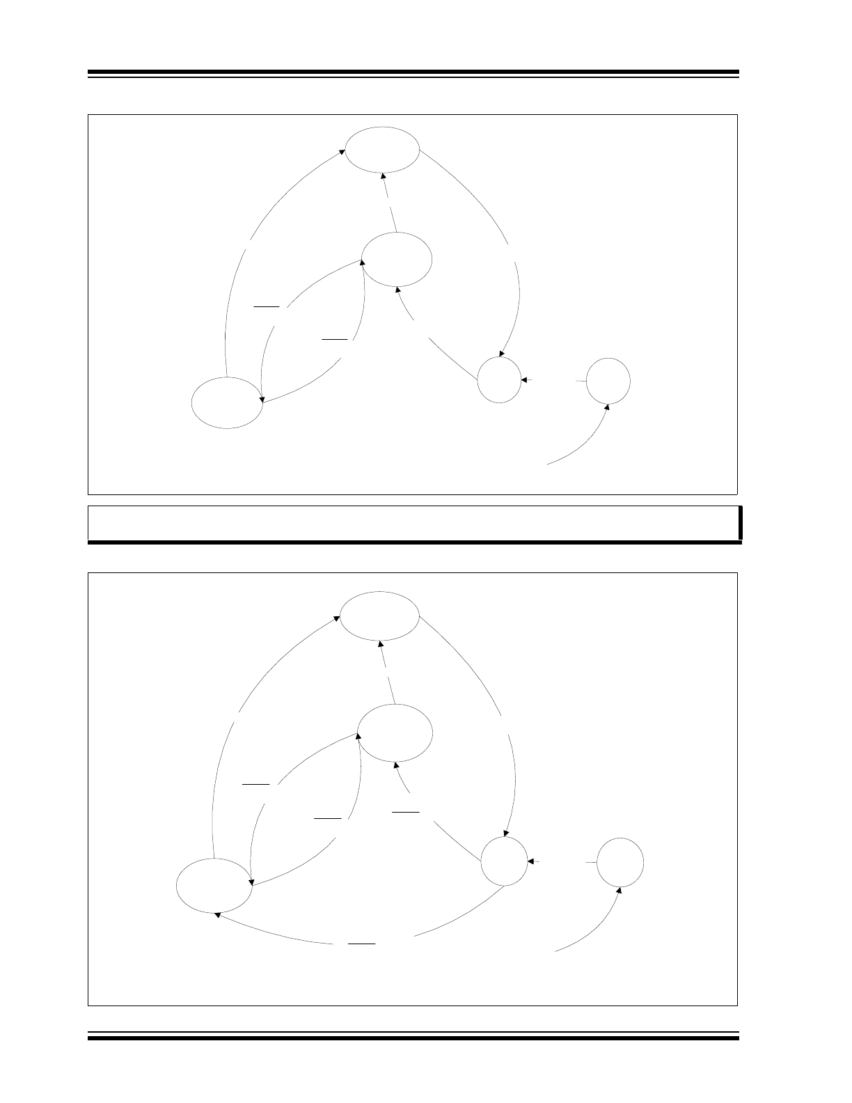
FIGURE 1-2:
MCP2021/2 OPERATIONAL MODES STATE DIAGRAM
FIGURE 1-3:
MCP2021P/2P OPERATIONAL MODES DIAGRAMS
Power-Down
TX: OFF
RX: OFF
V
REG
: OFF
CS/LWAKE =
0
Transmitter Off
TX: OFF
RX: ON
V
REG
: ON
POR
TX: OFF
RX: OFF
V
REG
: OFF
Operation
TX: ON
RX: ON
V
REG
: ON
Ready
TX: OFF
RX: ON
V
REG
: ON
V
BAT
> 5.75V
CS/LWAKE =
1&
VREG_OK =
1
CS/LWAKE =
0
FAULT/T
XE
=
0
Or Faults*
FAULT/T
XE
=
1
&No Faults*
CS/LWAKE =
1
or dominant level on L
BUS
Start
*Fault: thermal shutdown and T
XD
/L
BUS
permanent dominant
Note:
While the device is in shutdown, T
XD
should not be actively driven high or it may power internal logic
through the ESD diodes and may damage the device.
Power-Down
TX: OFF
RX: OFF
V
REG
: OFF
CS/LWAKE =
0
Transmitter Off
TX: OFF
RX: ON
V
REG
: ON
POR
TX: OFF
RX: OFF
V
REG
: OFF
Operation
TX: ON
RX: ON
V
REG
: ON
Ready
TX: OFF
RX: ON
V
REG
: ON
V
BAT
> 5.75V
CS/LWAKE =
1&
V
REG
_OK =
1&
FAULT/T
XE
=
1
CS/LWAKE =
0
FAULT/T
XE
=
0
Or Faults*
FAULT/T
XE
=
1
&No Faults*
CS/LWAKE =
1
or Falling edge on L
BUS
Start
*Fault: thermal shutdown and T
XD
/L
BUS
permanent dominant
CS =
1& V
REG
_OK =
1
&FAULT/T
XE
=
0
2005-2014 Microchip Technology Inc.
DS20002018H-page 9
MCP2021/2/1P/2P
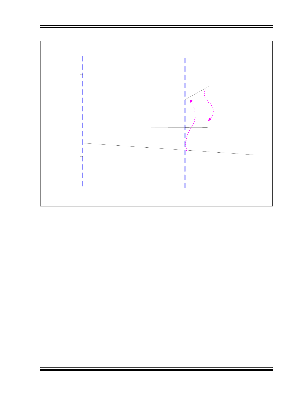
FIGURE 1-4:
MCP2021P/2P WAKE-UP DUE TO BUS DISCONNECTING
Ready
State
Sleep
0
L
BUS
FAULT
T
XE
V
REG
CS
LWAKE
0
MCP2021/2/1P/2P
DS20002018H-page 10
2005-2014 Microchip Technology Inc.
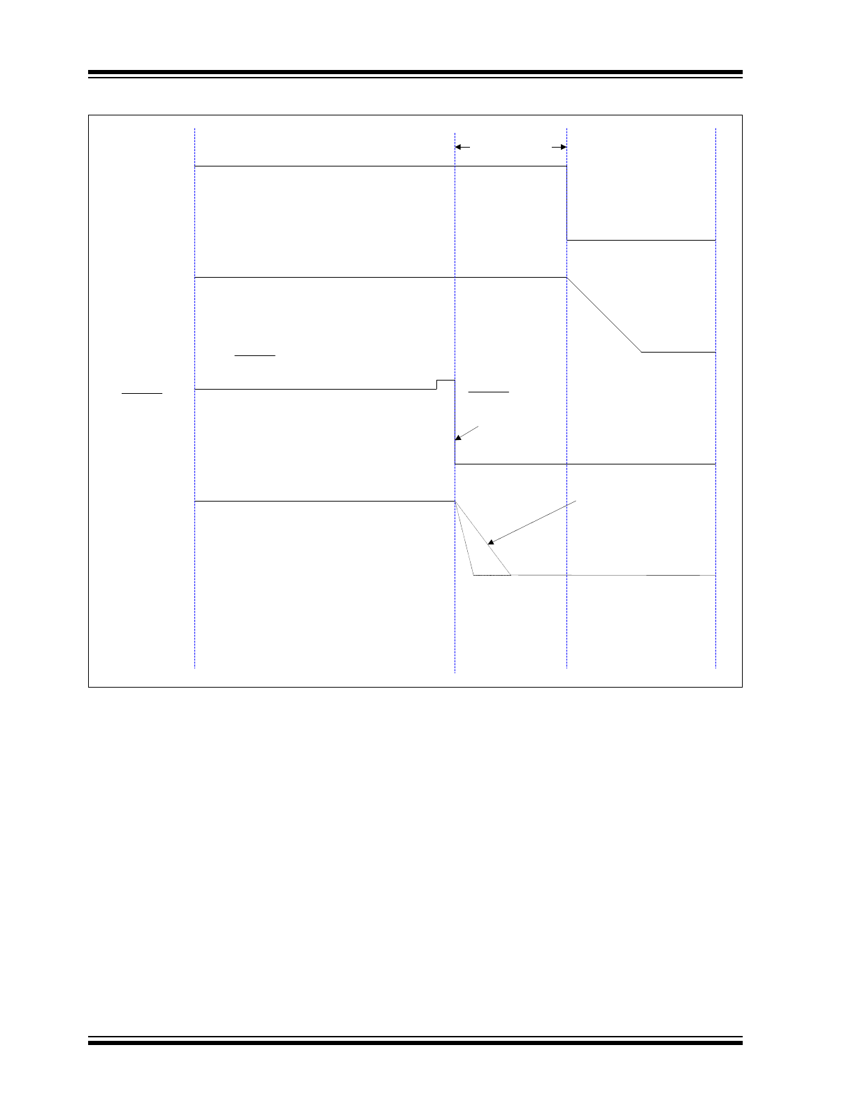
FIGURE 1-5:
FORCED POWER-DOWN MODE SEQUENCE FOR MCP2021P/2P
CS/LWAKE
V
REG
FAULT/T
XE
L
BUS
Operation Mode
Transmitter-Off
Mode
Power-Down
Mode
t
CSactive
> = 2
V
FAULT/T
XE
=
1
Forced internally
FAULT/T
XE
=
0
Forced externally
L
BUS
disconnected;
e.g., Master pull-up &
internal resistor off;
L
BUS
floating.
Forced Power-Down Mode after BUS-OFF
instruction or a longer LIN-Bus inactivity
( > = 4 sec according to LIN specification)
STATE