
2016 Microchip Technology Inc.
DS20005651A-page 1
MM5450/51
Features
• Continuous Brightness Control
• Serial Data Input
• No Load Signal Requirement
• Enable (MM5450 Only)
• Wide Power Supply Operation
• TTL Compatibility
• 34 or 35 Outputs, 15 mA Capability
• Alphanumeric Capability
Applications
• Industrial Control Indicator
• Relay Driver
• Digital Clock, Thermometer, Counter, Voltmeter
• Instrumentation Readouts
General Description
The MM5450 and MM5451 LED display drivers are
monolithic MOS IC’s fabricated in an N-Channel,
metal-gate process. The technology produces
low-threshold, enhancement-mode, and ion-implanted
depletion-mode devices.
A single pin controls the LED display brightness by
setting a reference current through a variable resistor
connected to the supply.
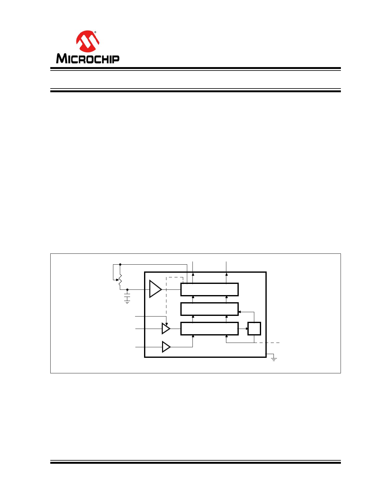
Block Diagram
35 OUTPUT BUFFERS
35 LATCHES
35-BIT SHIFT
REGISTER
LOAD
RESET
RESET
(only available
in die form)
SERIAL DATA
22
CLOCK
21
DATA ENABLE/OUT 35
(See Note 1)
23
19
20
24
OUT 34
18
OUT 1
1
BRIGHTNESS
CONTROL
VDD
Note 1: Pin in Data Enable in MM5450
Pin in Output 25 in MM5451
LED Display Driver
MM5450/51
DS20005651A-page 2
2016 Microchip Technology Inc.
Connection Diagram: Die
V
OUTPUT BIT 24
MM5450/5451
DIE PINOUT
OUTPUT BIT 25
OUTPUT BIT 26
OUTPUT BIT 27
OUTPUT BIT 28
OUTPUT BIT 29
OUTPUT BIT 30
OUTPUT BIT 31
OUTPUT BIT 32
OUTPUT BIT 33
SS
V
OUTPUT
BIT
13
OUTPUT
BIT
14
OUTPUT
BIT
15
OUTPUT
BIT
16
OUTPUT
BIT
17
OUTPUT
BIT
22
OUTPUT
BIT
23
OUTPUT
BIT
18
OUTPUT
BIT
19
OUTPUT
BIT
20
OUTPUT
BIT
21
SS
V SS
OUTPUT BIT 12
OUTPUT BIT 11
OUTPUT BIT 10
OUTPUT BIT 9
OUTPUT BIT 8
OUTPUT BIT 7
OUTPUT BIT 6
OUTPUT BIT 5
OUTPUT BIT 4
OUTPUT BIT 3
V
OUTPUT
BIT
34
OUTPUT
BIT
35
ENABLE
D
ATA
CLK
BRIGTNESS CONTROL
RESET
OUTPUT
BIT
1
OUTPUT
BIT
2
DD
2016 Microchip Technology Inc.
DS20005651A-page 3
MM5450/51
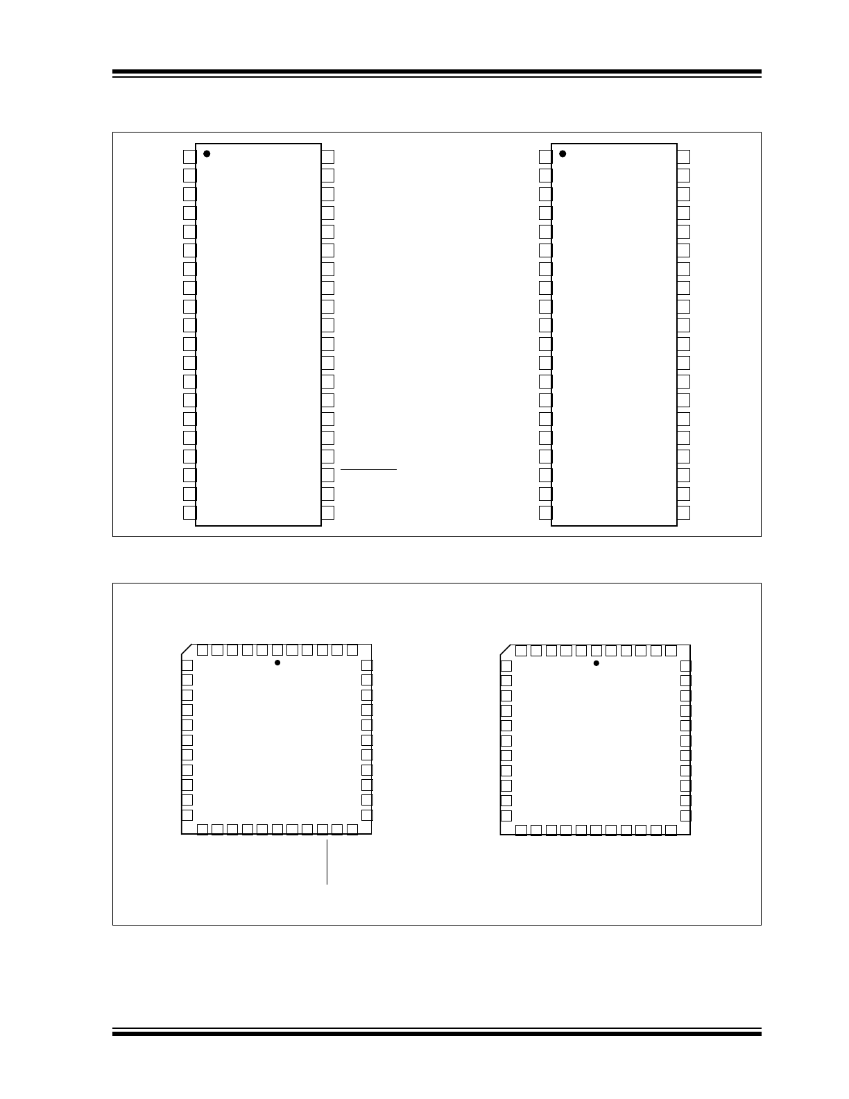
Connection Diagram: Dual-Inline Package (DIP)
Connection Diagram: Plastic-Leaded Chip Carrier (PLCC)
1
40
2
39
3
38
4
37
5
36
6
35
7
34
8
33
9
32
10
31
11
30
12
29
13
28
14
27
15
26
16
25
17
24
18
23
19
22
20
21
OUTPUT BIT 18
CLOCK IN
MM5450YN
V SS
V DD
OUTPUT BIT 17
OUTPUT BIT 16
OUTPUT BIT 15
OUTPUT BIT 14
OUTPUT BIT 13
OUTPUT BIT 12
OUTPUT BIT 11
OUTPUT BIT 10
OUTPUT BIT 9
OUTPUT BIT 8
OUTPUT BIT 7
OUTPUT BIT 6
OUTPUT BIT 5
OUTPUT BIT 4
OUTPUT BIT 3
OUTPUT BIT 2
OUTPUT BIT 1
BRIGHTNESS
CONTROL
DATA IN
DATA ENABLE
OUTPUT BIT 19
OUTPUT BIT 20
OUTPUT BIT 21
OUTPUT BIT 22
OUTPUT BIT 23
OUTPUT BIT 24
OUTPUT BIT 25
OUTPUT BIT 26
OUTPUT BIT 27
OUTPUT BIT 28
OUTPUT BIT 29
OUTPUT BIT 30
OUTPUT BIT 31
OUTPUT BIT 32
OUTPUT BIT 33
OUTPUT BIT 34
1
40
2
39
3
38
4
37
5
36
6
35
7
34
8
33
9
32
10
31
11
30
12
29
13
28
14
27
15
26
16
25
17
24
18
23
19
22
20
21
OUTPUT BIT 18
CLOCK IN
MM5451YN
V SS
V DD
OUTPUT BIT 17
OUTPUT BIT 16
OUTPUT BIT 15
OUTPUT BIT 14
OUTPUT BIT 13
OUTPUT BIT 12
OUTPUT BIT 11
OUTPUT BIT 10
OUTPUT BIT 9
OUTPUT BIT 8
OUTPUT BIT 7
OUTPUT BIT 6
OUTPUT BIT 5
OUTPUT BIT 4
OUTPUT BIT 3
OUTPUT BIT 2
OUTPUT BIT 1
BRIGHTNESS
CONTROL
DATA IN
OUTPUT BIT 19
OUTPUT BIT 20
OUTPUT BIT 21
OUTPUT BIT 22
OUTPUT BIT 23
OUTPUT BIT 24
OUTPUT BIT 25
OUTPUT BIT 26
OUTPUT BIT 27
OUTPUT BIT 28
OUTPUT BIT 29
OUTPUT BIT 30
OUTPUT BIT 31
OUTPUT BIT 32
OUTPUT BIT 33
OUTPUT BIT 34
OUTPUT BIT 35
1
2
39
3
38
4
37
5
36
7
35
8
34
9
33
10
32
11
31
12
30
13
29
14
15
16
17
MM5450YV
V
SS
OUTPUT
BIT
15
OUTPUT
BIT
14
OUTPUT
BIT
16
OUTPUT
BIT
17
OUTPUT BIT 13
OUTPUT BIT 12
OUTPUT BIT 11
OUTPUT BIT 10
OUTPUT BIT 9
OUTPUT BIT 8
OUTPUT BIT 7
OUTPUT BIT 6
OUTPUT BIT 5
OUTPUT BIT 4
OUTPUT BIT 23
OUTPUT BIT 24
OUTPUT BIT 25
OUTPUT BIT 26
OUTPUT BIT 27
NC
OUTPUT BIT 28
OUTPUT BIT 29
OUTPUT BIT 30
OUTPUT BIT 31
OUTPUT BIT 32
NC
6
44
43
42
41
40
NC
OUTPUT
BIT
18
OUTPUT
BIT
19
OUTPUT
BIT
20
OUTPUT
BIT
21
OUTPUT
BIT
3
OUTPUT
BIT
2
OUTPUT
BIT
1
BRIGHTNESS CONTROL
NC
CLOCK IN
D
ATA
I
N
DA
T
A
ENABLE
OUTPUT
BIT
34
OUTPUT
BIT
33
23
22
21
20
19
18
24
25
26
27
28
OUTPUT
BIT
22
V
DD
1
2
39
3
38
4
37
5
36
7
35
8
34
9
33
10
32
11
31
12
30
13
29
14
15
16
17
MM5451YV
V
SS
OUTPUT
BIT
14
OUTPUT
BIT
15
OUTPUT
BIT
16
OUTPUT
BIT
17
OUTPUT BIT 13
OUTPUT BIT 12
OUTPUT BIT 11
OUTPUT BIT 10
OUTPUT BIT 9
OUTPUT BIT 8
OUTPUT BIT 7
OUTPUT BIT 6
OUTPUT BIT 5
OUTPUT BIT 4
OUTPUT BIT 23
OUTPUT BIT 24
OUTPUT BIT 25
OUTPUT BIT 26
OUTPUT BIT 27
NC
OUTPUT BIT 28
OUTPUT BIT 29
OUTPUT BIT 30
OUTPUT BIT 31
OUTPUT BIT 32
NC
6
44
43
42
41
40
NC
OUTPUT
BIT
18
OUTPUT
BIT
19
OUTPUT
BIT
20
OUTPUT
BIT
21
OUTPUT
BIT
3
OUTPUT
BIT
2
OUTPUT
BIT
1
BRIGHTNESS CONTROL
NC
CLOCK IN
D
ATA
I
N
OUTPUT
BIT
35
OUTPUT
BIT
34
OUTPUT
BIT
33
23
22
21
20
19
18
24
25
26
27
28
OUTPUT
BIT
22
V
DD

MM5450/51
DS20005651A-page 4
2016 Microchip Technology Inc.
1.0
ELECTRICAL CHARACTERISTICS
Absolute Maximum Ratings †
Voltage (Any Pin)................................................................................................................................... V
SS
to V
SS
+ 12V
Power Dissipation (+25°C) ...........................................................................................................................................1W
Power Dissipation (+85°C) ...................................................................................................................................560 mW
Operating Ratings ‡
Supply Voltage (V
DD
– V
SS
) ..................................................................................................................... +4.75V to +11V
†
Notice: Stresses above those listed under “Absolute Maximum Ratings” may cause permanent damage to the device.
This is a stress rating only and functional operation of the device at those or any other conditions above those indicated
in the operational sections of this specification is not intended. Exposure to maximum rating conditions for extended
periods may affect device reliability.
‡ Notice:
The device is not guaranteed to function outside its operating ratings.
2016 Microchip Technology Inc.
DS20005651A-page 5
MM5450/51
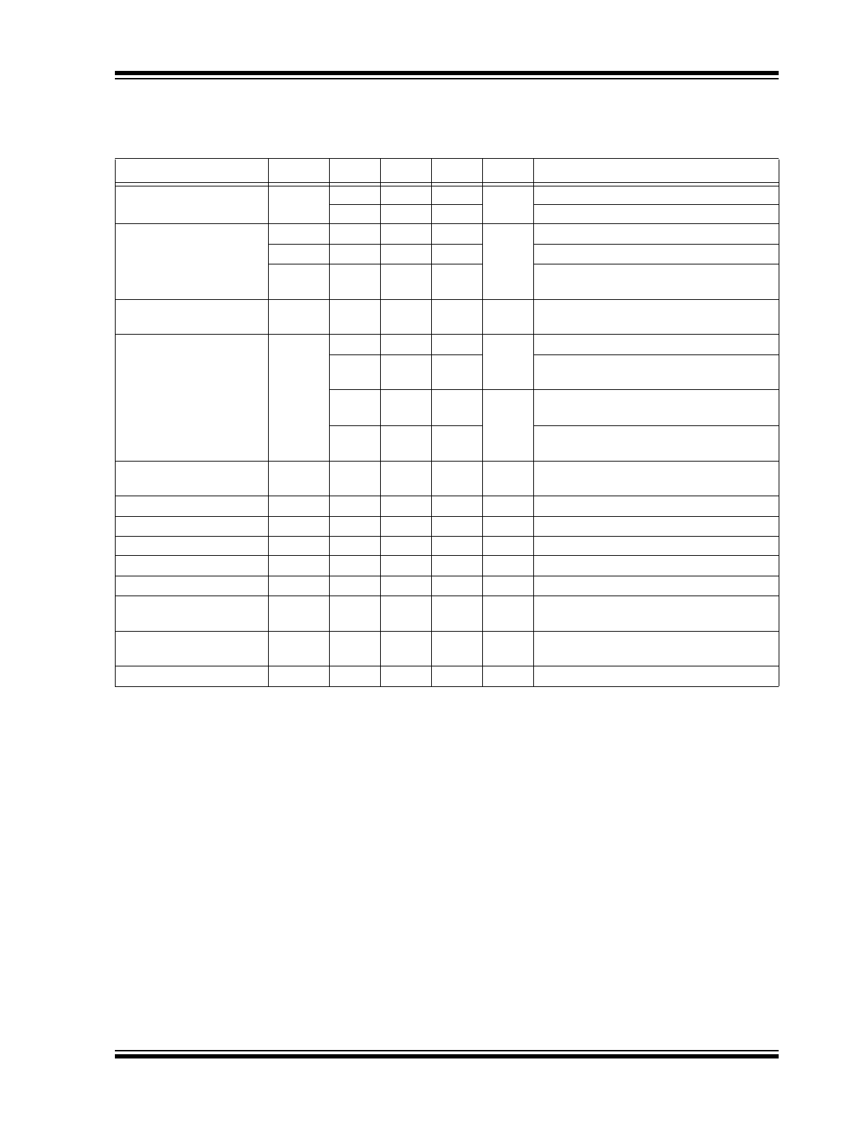
TABLE 1-1:
ELECTRICAL CHARACTERISTICS
Electrical Characteristics:
4.5V ≤ V
DD
≤ 11V, V
SS
= 0V; T
A
= 25°C, bold values valid for –40°C ≤ T
A
≤ +85°C,
unless otherwise noted.
Parameter
Symbol
Min.
Typ.
Max.
Units
Conditions
Power Supply Current
—
—
—
8.5
mA
–25°C to +85°C, excluding output loads
—
—
10
–40°C to +85°C, excluding output loads
Data Input Voltage
V
L
–0.3
—
0.8
V
Logic-0 level, ±10 µA input bias
V
H
2.2
—
V
DD
Logic-1 level, 4.75V ≤ V
DD
≤ 5.25V
—
V
DD
–
2
—
V
DD
V
DD
> 5.25V
Brightness Control Input
Current
—
0
—
0.75
mA
Note 1
Output Sink Current
—
—
—
10
µA
Segment off, V
OUT
= 3.0V
0
—
10
Segment on, V
OUT
= 1.8V,
Note 2
;
Brightness input = 0 µA
2.0
2.7
4
mA
Segment on, V
OUT
= 1.8V,
Note 2
;
Brightness input = 100 µA
15
—
25
Segment on, V
OUT
= 1.8V,
Note 2
;
Brightness input = 750 µA
Brightness Control Input
Voltage
—
3.0
—
4.3
V
Input current = 750 µA
Output Matching
—
—
—
±20
%
Note 3
,
Note 4
Clock Input Frequency
f
C
—
—
500
kHz
Note 5
,
Note 6
Clock Input High Time
t
H
950
—
—
ns
Note 5
,
Note 6
Clock Input Low Time
t
L
950
—
—
ns
Note 5
,
Note 6
Data Input Setup Time
t
DS
300
—
—
ns
—
Data Input Hold Setup
Time
t
DH
300
—
—
ns
—
Data Enable Input Setup
Time
t
DES
100
—
—
ns
—
Reset Pad Current
—
–8
—
8
µA
Die.
Note 1:
With a fixed resistor on the brightness input pin, some variation in brightness will occur among devices.
2:
See
Figure 2-1
,
Figure 2-2
, and
Figure 2-3
for recommended operating conditions and limits. Absolute
maximum for each output should be limited to 40 mA.
3:
Output matching is calculated as the percent variation of (I
MAX
+ I
MIN
) / 2.
4:
V
OUT
should be regulated by user. See
Figure 2-2
and
Figure 2-3
for allowable V
OUT
vs. I
OUT
operation.
5:
AC input waveform specification for test purpose: t
R
≤ 200 ns, t
F
≤ 20 ns, f = 500 kHz, 50% ±10% duty
cycle.
6:
Clock input rise and fall times must not exceed 300 ns.

MM5450/51
DS20005651A-page 6
2016 Microchip Technology Inc.
TEMPERATURE SPECIFICATIONS (
Note 1
)
Parameters
Sym.
Min.
Typ.
Max.
Units
Conditions
Temperature Ranges
Ambient Temperature Range
T
A
–40
—
+85
°C
—
Storage Temperature Range
T
S
–65
—
+150
°C
—
Junction Temperature
T
J
—
—
+150
°C
—
Lead Temperature
—
—
—
+300
°C
—
Note 1:
The maximum allowable power dissipation is a function of ambient temperature, the maximum allowable
junction temperature and the thermal resistance from junction to air (i.e., T
A
, T
J
,
JA
). Exceeding the
maximum allowable power dissipation will cause the device operating junction temperature to exceed the
maximum +125°C rating. Sustained junction temperatures above +125°C can impact the device reliability.
2016 Microchip Technology Inc.
DS20005651A-page 7
MM5450/51
2.0
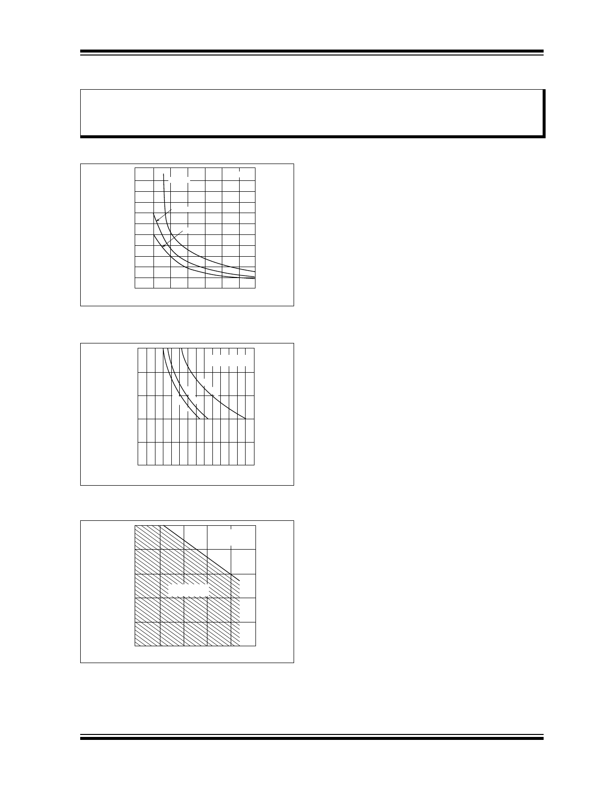
TYPICAL PERFORMANCE CURVES
FIGURE 2-1:
Output Current vs. Number
of Segments.
FIGURE 2-2:
Output Voltage vs. LED
Current.
FIGURE 2-3:
Power Dissipation vs.
Temperature.
Note:
The graphs and tables provided following this note are a statistical summary based on a limited number of
samples and are provided for informational purposes only. The performance characteristics listed herein
are not tested or guaranteed. In some graphs or tables, the data presented may be outside the specified
operating range (e.g., outside specified power supply range) and therefore outside the warranted range.
110
100
90
80
70
60
50
40
30
20
10
0
0
5
10
15
20
25
30
35
NUMBER OF SEGMENTS
OUTPUT
CURRENT
(mA)
V = 1V
OUT
V = 1.5V
OUT
V = 2V
OUT
T = 85°C
A
2.5
2.0
1.5
1.0
0.5
0
0
4
8
12
16
20
24
28
I (mA)
LED
V (V )
OUT
O
T = 85°C
T = 150°C (MAX)
A
J
20 SEGM
30 SEGM
34 SEGM
1.0
0.8
0.6
0.4
0.2
0
0
20
40
60
80
TEMPERATURE (°C)
POWER DISSIP
A
TION (W)
34 SEGMENTS
V = 1V
15 mA/SEGMENT
OUT
SAFE OPERATING
AREA
100
MM5450/51
DS20005651A-page 8
2016 Microchip Technology Inc.
3.0
FUNCTIONAL DESCRIPTION
The MM5450 and MM5451 are designed to drive either
4- or 5-digit alphanumeric LED displays with the added
benefit of requiring minimal interface with the display or
data source.
Data is transferred serially via two signals: clock and
serial data. Data transfer without the added
inconvenience of an external load signal is
accomplished by using a format of a leading “1”
followed by the allowed 35 data bits. These 35 data bits
are latched after the 36th has been transferred. This
scheme provides non-multiplexed, direct drive to the
LED display. Characters currently displayed (thus, data
output) changes only if the serial data bits differ from
those previously transferred.
Control of the output current for LED displays provides
for the display brightness. To prevent oscillations, a
1 nF capacitor should be connected to pin 19,
brightness control.
The
Block Diagram
is shown on page 1. For the
MIC5450, the /DATA ENABLE is a metal option and is
used instead of the 35th output. The output current is
typically 20-times greater than the current into pin 19,
which is set by an external variable resistor.
There is an external reset connection shown which is
available on unpackaged (die) only.
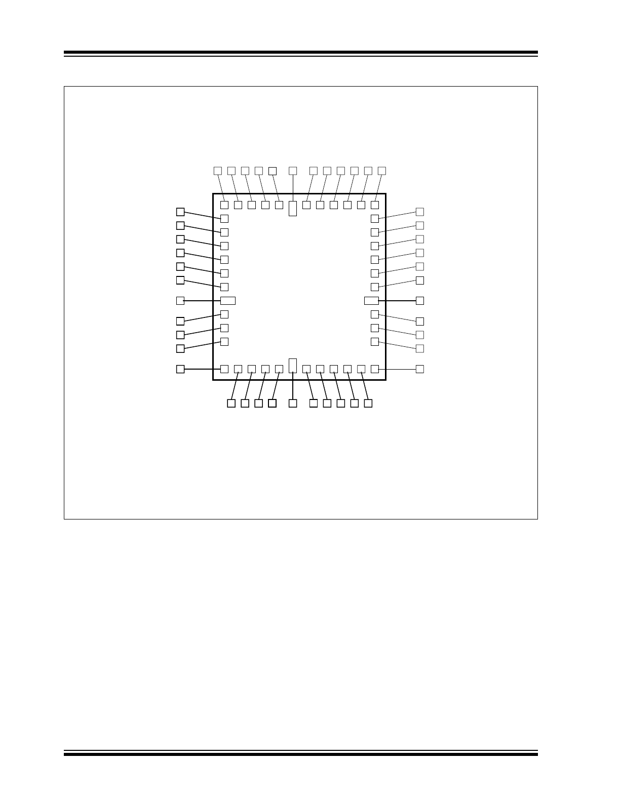
Connection
Diagram: Die
illustrates the die pad locations for
bonding in “chip on board” applications.
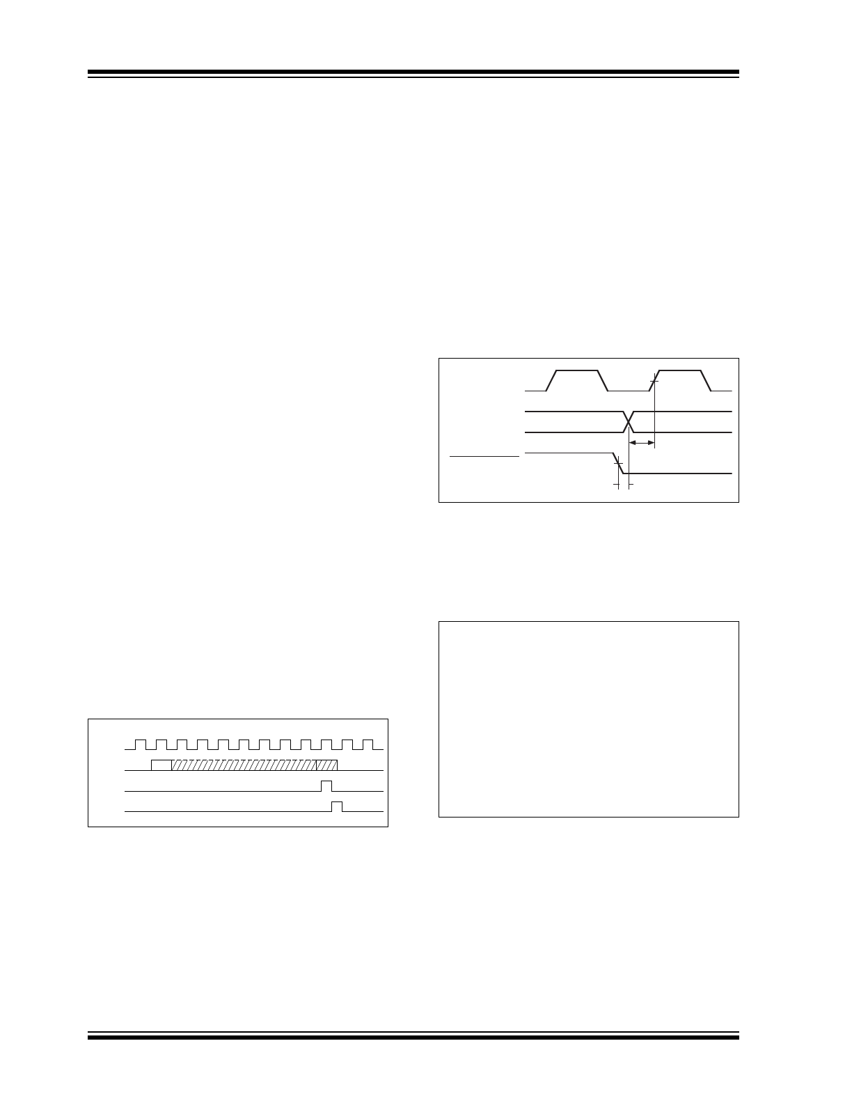
Figure 3-1
shows the input data format. A leading “1” is
followed by 35 bits of data. After the 36th had been
transferred, a LOAD signal is generated synchronously
with the clock high state. This loads the 35 bits of data
into the latches. The low side of the clock is used to
generate a RESET signal which clears all shift registers
for the next set of data. All shift registers are static
master-slave, with no clear for the master portion of the
first register, allowing continuous operation.
FIGURE 3-1:
Input Data Format.
There must be a complete set of 36 clocks or the shift
registers will not clear.
When the chip first powers ON, an internal power ON
reset signal is generated that resets all registers and all
latches. The START bit and the first clock return the
chip to its normal operation.
The
Connection Diagram: Dual-Inline Package (DIP)
and
Connection Diagram: Plastic-Leaded Chip Carrier
(PLCC)
show the pinout of the MIC5450 and MIC5451.
Bit 1 is the first bit following the start bit and it will
appear on pin 18. A logical “1” at the input will turn on
the appropriate LED.
Figure 3-2
shows the timing relationships between
data, clock and /DATA ENABLE. A maximum clock
frequency of 0.5 MHz is assumed.
FIGURE 3-2:
Timing Diagram.
For applications where a lesser number of outputs is
used, it is possible to either increase the current per
output, or operate the part at higher than 1V V
OUT
. The
following equation can be used for calculations.
EQUATION 3-1:
Equation 3-1
is used to plot
Figure 2-1
,
Figure 2-2
, and
Figure 2-3
.
CLOCK
1
DATA
LOAD
(INTERNAL)
RESET
(INTERNAL)
START BIT 1
BIT 36
36
37
BIT 35
CLOCK
DATA
DATA ENABLE
300 nS MIN
100 nS MIN
T
J
V
OUT
I
LED
No of segments
124
o
C/W
T
A
+
=
Where:
T
J
Junction Temperature (+150°C max.)
V
OUT
Voltage at the LED driver outputs
I
LED
LED current
124°C/W Thermal resistance of the package
T
A
Ambient temperature
2016 Microchip Technology Inc.
DS20005651A-page 9
MM5450/51
4.0
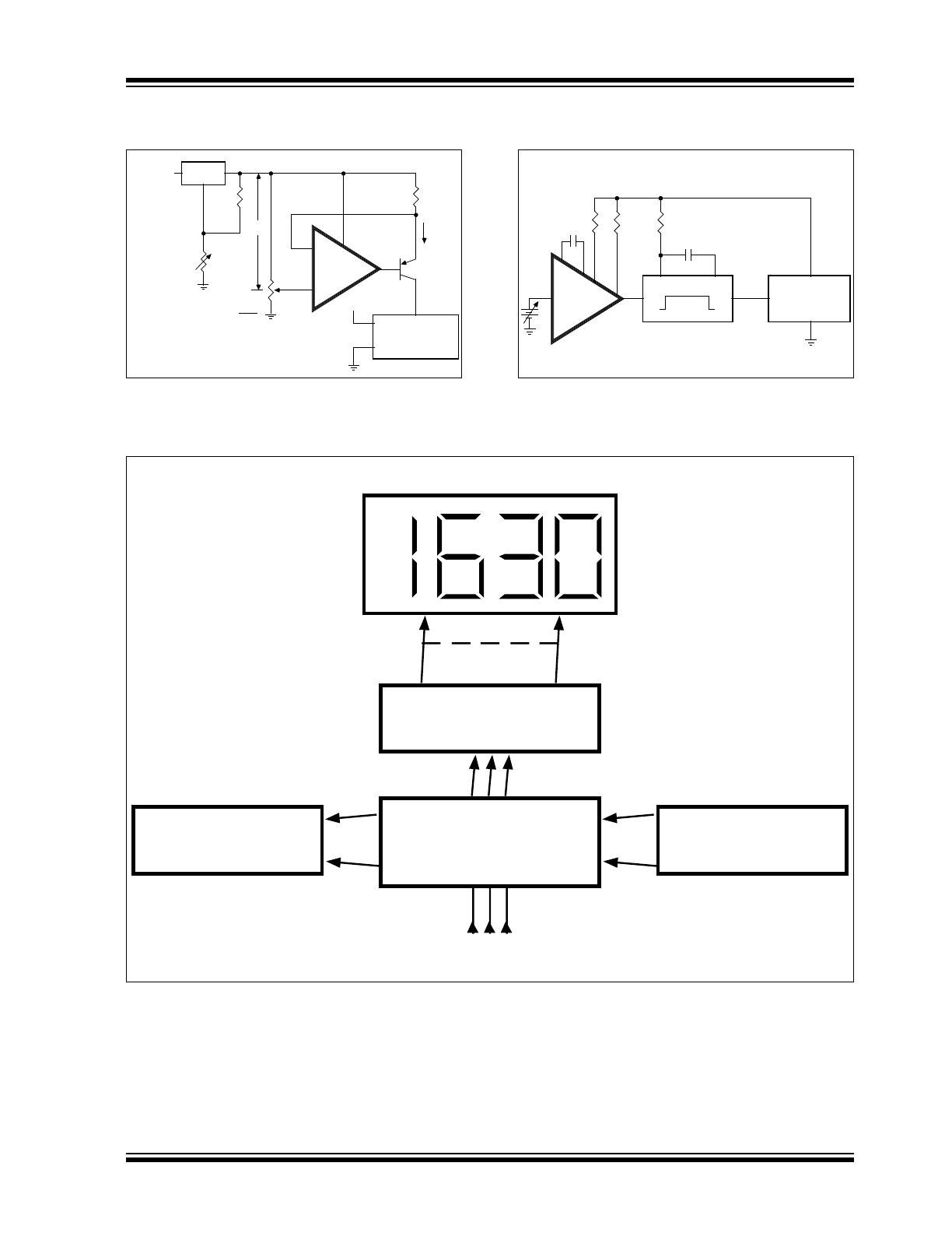
TYPICAL APPLICATIONS
FIGURE 4-1:
Typical Application of
Constant Current Brightness Control.
FIGURE 4-2:
Brightness Control Varying
the Duty Cycle.
FIGURE 4-3:
Basic Electronically Tuned Radio System.
LM324
MM5450
LM317
–
+
¨9
240
ȍ
RAW DC
!9
¨9
1K
I19 =
2N2907
I19
PIN 19
9
20
1
5k
9
1k
CD4046
(VCO)
5V
MM74HC123
10 μS
MM5450
Q 19
20
1
LED DISPLAY
34
MM5450
DISPLAY DRIVER
ELECTRONIC
TUNING
CONTROLLER
PLL
SYNTHESIZER
KEYBOARD
STATION DETECT, ETC.
AM
FM
MM5450/51
DS20005651A-page 10
2016 Microchip Technology Inc.
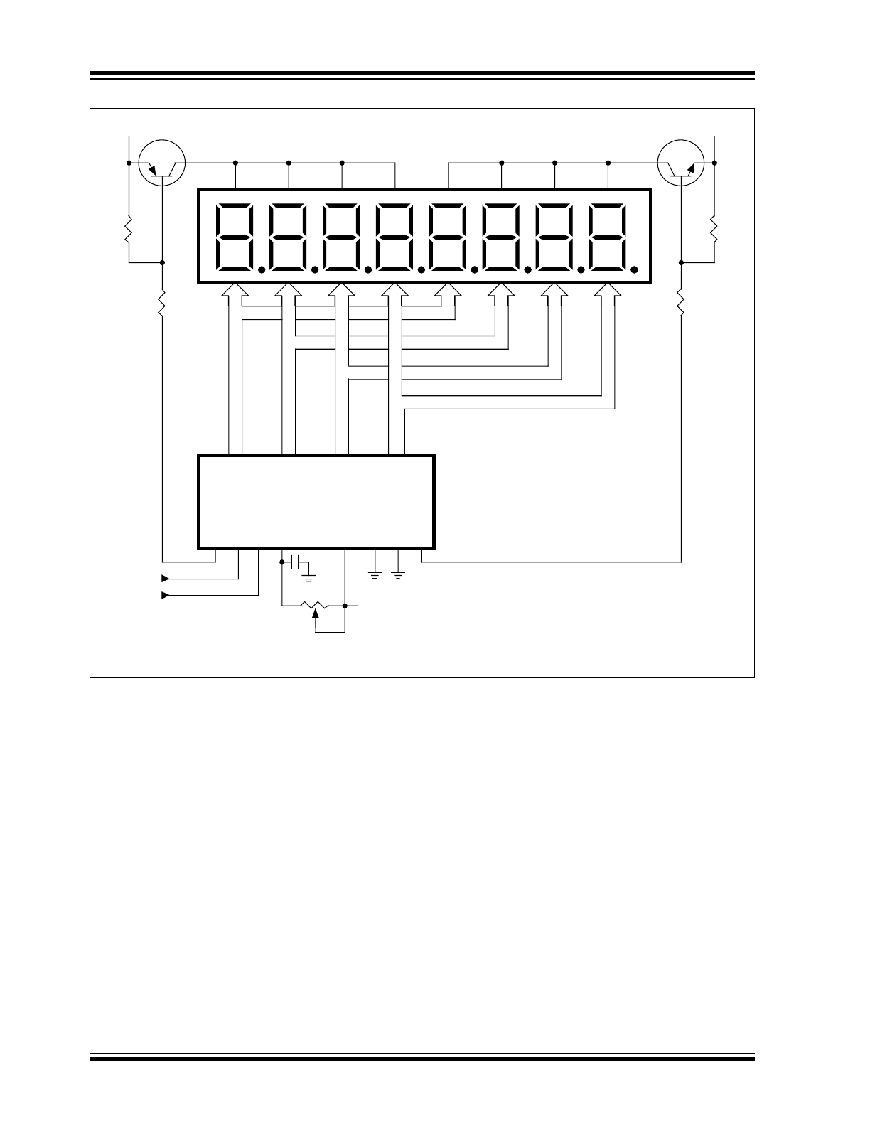
FIGURE 4-4:
Duplexing Eight Digits with One MM5450.
9–16
2–8, 40 32–39
24–31
18 21 22 19
20
1 23 17
100k
TYP.
MM5450
V
LED
V
LED
V
LED
= 3.0V
V
LED
= 3.0V
CLOCK IN
DATA IN
V
DD
BRIGHTNESS
CONTROL