

2012-2015 Microchip Technology Inc.
DS00001946A-page 1
Highlights
• Single Chip HSIC USB 2.0 to 10/100 Ethernet
Controller
• Integrated 10/100 Ethernet MAC with Full-Duplex
Support
• Integrated 10/100 Ethernet PHY with HP Auto-
MDIX Support
• Integrated USB 2.0 Hi-Speed Device Controller
• Integrated HSIC Interface
• Implements Reduced Power Operating Modes
Target Applications
• Embedded Systems
• Set-Top Boxes
• PVRs
• CE Devices
• Networked Printers
• USB Port Replicators
• Test Instrumentation
• Industrial
Key Features
• USB Device Controller
- Fully compliant with Hi-Speed Universal Serial
Bus Specification, revision 2.0
- Supports HS (480 Mbps) mode
- Four Endpoints supported
- Supports vendor specific commands
- Integrated HSIC Interface
- Remote wakeup supported
• High-Performance 10/100 Ethernet Controller
- Fully compliant with IEEE 802.3/802.3u
- Integrated Ethernet MAC and PHY
- 10BASE-T and 100BASE-TX support
- Full- and half-duplex support
- Full- and half-duplex flow control
- Preamble generation and removal
- Automatic 32-bit CRC generation and checking
- Automatic payload padding and pad removal
- Loop-back modes
- TCP/UDP/IP/ICMP checksum offload support
- Flexible address filtering modes
- One 48-bit perfect address
- 64 hash-filtered multicast addresses
- Pass all multicast
- Promiscuous mode
- Inverse filtering
- Pass all incoming with status report
- Wakeup packet support
- Integrated Ethernet PHY
- Auto-negotiation
- Automatic polarity detection and correction
- HP Auto-MDIX support
- Link status change wake-up detection
- Support for three status LEDs
- External MII and Turbo MII support HomePNA
®
and HomePlug
®
PHY
• Power and I/Os
- Various low power modes
- Supports PCI-like PME wake when USB host dis-
abled
- 11 GPIOs
- Supports bus-powered and self-powered opera-
tion
- Integrated power-on reset circuit
- Single external 3.3 V I/O supply
- Optional internal core regulator
• Miscellaneous Features
- EEPROM controller
- Supports custom operation without EEPROM
- IEEE 1149.1 (JTAG) boundary scan
- Requires single 25 MHz crystal
• Software
- Windows
®
8/7/XP/Vista driver
- Linux
®
driver
- Win CE driver
- MAC
®
OS driver
- EEPROM utility
• Packaging
- 56-pin VQFN (8 x 8 mm), RoHS-compliant
• Environmental
- Commercial Temperature Range (0°C to +70°C)
- Industrial Temperature Range (-40°C to +85°C)
LAN9730/LAN9730i
High-Speed Inter-Chip (HSIC) USB 2.0 to 10/100 Ethernet
Controller

LAN9730/LAN9730i
DS00001946A-page 2
2012-2015 Microchip Technology Inc.
TO OUR VALUED CUSTOMERS
It is our intention to provide our valued customers with the best documentation possible to ensure successful use of your Microchip
products. To this end, we will continue to improve our publications to better suit your needs. Our publications will be refined and
enhanced as new volumes and updates are introduced.
If you have any questions or comments regarding this publication, please contact the Marketing Communications Department via
E-mail at
docerrors@microchip.com
. We welcome your feedback.
Most Current Data Sheet
To obtain the most up-to-date version of this data sheet, please register at our Worldwide Web site at:
http://www.microchip.com
You can determine the version of a data sheet by examining its literature number found on the bottom outside corner of any page.
The last character of the literature number is the version number, (e.g., DS30000000A is version A of document DS30000000).
Errata
An errata sheet, describing minor operational differences from the data sheet and recommended workarounds, may exist for current
devices. As device/documentation issues become known to us, we will publish an errata sheet. The errata will specify the revision
of silicon and revision of document to which it applies.
To determine if an errata sheet exists for a particular device, please check with one of the following:
• Microchip’s Worldwide Web site:
http://www.microchip.com
• Your local Microchip sales office (see last page)
When contacting a sales office, please specify which device, revision of silicon and data sheet (include -literature number) you are
using.
Customer Notification System
Register on our web site at
www.microchip.com
to receive the most current information on all of our products.

2012-2015 Microchip Technology Inc.
DS00001946A-page 3
LAN9730/LAN9730i
Table of Contents
1.0 Introduction ..................................................................................................................................................................................... 5
2.0 Pin Description and Configuration ................................................................................................................................................ 11
3.0 Power Connections ....................................................................................................................................................................... 27
4.0 Functional Description .................................................................................................................................................................. 29
5.0 PME Operation ........................................................................................................................................................................... 115
6.0 Register Descriptions .................................................................................................................................................................. 119
7.0 Operational Characteristics ......................................................................................................................................................... 195
8.0 Packaging Information ................................................................................................................................................................ 213
The Microchip Web Site .................................................................................................................................................................... 219
Customer Change Notification Service ............................................................................................................................................. 219
Customer Support ............................................................................................................................................................................. 219
Product Identification System ........................................................................................................................................................... 220

LAN9730/LAN9730i
DS00001946A-page 4
2012-2015 Microchip Technology Inc.
NOTES:

2012-2015 Microchip Technology Inc.
DS00001946A-page 5
LAN9730/LAN9730i
1.0
INTRODUCTION
1.1
General Terms
Byte
8 bits
CSR
Control and Status Registers
DWORD
32 bits
FCT
FIFO Controller
FIFO
First In First Out buffer
Frame
In the context of this document, a frame refers to transfers on the Ethernet
interface.
FSM
Finite State Machine
GPIO
General Purpose I/O
HSIC
High-Speed Inter-Chip
Host
External system (includes processor, application software, etc.)
Level-Triggered Sticky Bit
This type of status bit is set whenever the condition that it represents is
asserted. The bit remains set until the condition is no longer true and the sta-
tus bit is cleared by writing a zero.
LFSR
Linear Feedback Shift Register
MAC
Media Access Controller
MII
Media Independent Interface
N/A
Not Applicable
Packet
In the context of this document, a packet refers to transfers on the USB inter-
face.
POR
Power on Reset
RESERVED
Refers to a reserved bit field or address. Unless otherwise noted, reserved
bits must always be zero for write operations. Unless otherwise noted, values
are not ensured when reading reserved bits. Unless otherwise noted, do not
read or write to reserved addresses.
SCSR
System Control and Status Register
SMI
Serial Management Interface
TLI
Transaction Layer Interface
URX
USB Bulk-Out Packet Receiver
UTX
USB Bulk-In Packet Transmitter
WORD
16 bits
ZLP
Zero Length USB Packet
LAN9730/LAN9730i
DS00001946A-page 6
2012-2015 Microchip Technology Inc.
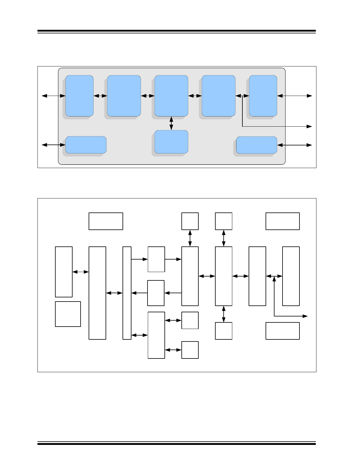
1.2
Block Diagram
FIGURE 1-1:
BLOCK DIAGRAM
FIGURE 1-2:
SYSTEM DIAGRAM
TAP
Controller
EEPROM
Controller
USB 2.0
Device
Controller
SRAM
Ethernet
PHY
10/100
Ethernet
MAC
FIFO
Controller
HSIC
Interface
LAN9730/LAN9730i
MII: To optional
external PHY
Ethernet
EEPROM
JTAG
HSIC
UDC
MAC
FCT
RAM
7kx32
TLI
Reg
File
512x37
Reg
File
32x37
EEPROM
Controller
ETH
PHY
HSIC
I/F
UTX
TAP
Controller
USB
Common
Block
URX
CTL
M
U
X
Reg
File
128x32
SCSR
CPM
MII: To optional
external PHY

2012-2015 Microchip Technology Inc.
DS00001946A-page 7
LAN9730/LAN9730i
1.2.1
OVERVIEW
The LAN9730/LAN9730i is a high performance solution for USB to 10/100 Ethernet port bridging. With applications
ranging from embedded systems, set-top boxes, and PVRs, to USB port replicators, and test instrumentation, the device
is targeted as a high-performance, low-cost USB/Ethernet connectivity solution.
The LAN9730/LAN9730i contains an integrated 10/100 Ethernet PHY, HSIC interface, Hi-Speed USB 2.0 device con-
troller, 10/100 Ethernet MAC, TAP controller, EEPROM controller, and a FIFO controller with a total of 30 kB of internal
packet buffering. Two kB of buffer memory are allocated to the Transaction Layer Interface (TLI), while 28 kB are allo-
cated to the FIFO Controller (FCT).
The internal USB 2.0 device controller is compliant with the USB 2.0 Hi-Speed standard. The HSIC interface is compliant
with the High-Speed Interchip USB Electrical Specification Revision 1.0. High-Speed Inter-Chip (HSIC) is a digital inter-
connect bus that enables the use of USB technology as a low-power chip-to-chip interconnect at speeds up to 480 Mb/
s. The device implements Control, Interrupt, Bulk-In and Bulk-Out USB Endpoints.
The Ethernet controller supports auto-negotiation, auto-polarity correction, HP Auto-MDIX, and is compliant with the
IEEE 802.3 and 802.3u standards. An external MII interface provides support for an external Fast Ethernet PHY, Home-
PNA, and HomePlug functionality.
Multiple power management features are provided, including various low-power modes, and Magic Packet, Wake On
LAN and Link Status Change wake events. These wake events can be programmed to initiate a USB remote wakeup.
A PCI-like PME wake is also supported when the host controller is disabled.
An internal EEPROM controller exists to load various USB configuration information and the device MAC address. The
integrated IEEE 1149.1 compliant TAP controller provides boundary scan via JTAG.
1.2.2
USB
The USB portion of the LAN9730/LAN9730i consists of the USB Device Controller (UDC), USB Bulk-Out Packet
Receiver (URX), USB Bulk-In Packet Transmitter (UTX), Control Block (CTL), System Control and Status Registers
(SCSR), and HSIC interface.
The USB device controller (UDC) contains a USB low-level protocol interpreter which implements the USB bus protocol,
packet generation/extraction, PID/Device ID parsing, and CRC coding/decoding with autonomous error handling. It has
autonomous protocol handling functions such as stall condition clearing on setup packets, suspend/resume/reset con-
ditions, and remote wakeup. It also autonomously handles contingency operations for error conditions such as retry for
CRC errors, Data toggle errors, and generation of NYET, STALL, ACK, and NACK depending on the Endpoint buffer
status. The UDC implements four USB Endpoints: Control, Interrupt, Bulk-In, and Bulk-Out.
The Control block (CTL) manages traffic to/from the control Endpoint that is not handled by the UDC and constructs the
packets used by the interrupt Endpoint. The CTL is responsible for handling some USB standard commands and all
vendor specific commands. The vendor specific commands allow for efficient statistics collection and access to the
SCSR.
The URX and UTX implement the Bulk-Out and Bulk-In pipes, respectively, which connect the USB host and the UDC.
They perform the following functions:
The URX passes USB Bulk-Out packets to the FIFO Controller (FCT). It tracks whether or not a USB packet is errone-
ous. It instructs the FCT to flush erroneous packets by rewinding its write pointer.
The UTX retrieves Ethernet frames from the FCT and constructs USB Bulk-In packets from them. If the handshake for
a transmitted Bulk-In packet does not complete, the UTX is capable of retransmitting the packet. The UTX will not
instruct the FCT to advance its read head pointer until the current USB packet has been successfully transmitted to the
USB host.
Both the URX and UTX are responsible for handling Ethernet frames encapsulated over USB by one of the following
methods:
• Multiple Ethernet frames per USB Bulk packet
• Single Ethernet frame per USB Bulk packet
The UDC also implements the System Control and Status Register (SCSR) space used by the host to obtain status and
control overall system operation.
The integrated HSIC interface is compliant with the High-Speed Interchip USB Electrical Specification Revision 1.0 (09-
23-07) and supports the Hi-Speed mode of operation.

LAN9730/LAN9730i
DS00001946A-page 8
2012-2015 Microchip Technology Inc.
1.2.3
FIFO CONTROLLER (FCT)
The FIFO controller uses a 28 kB internal SRAM to buffer RX and TX traffic. 20 kB are allocated for received Ethernet-
USB traffic (RX buffer), while 8 kB are allocated for USB-Ethernet traffic (TX buffer). Bulk-Out packets from the USB
controller are directly stored into the TX buffer. The FCT is responsible for extracting Ethernet frames from the USB
packet data and passing the frames to the MAC. Ethernet frames are directly stored into the RX buffer and become the
basis for Bulk-In packets. The FCT passes the stored data to the UTX in blocks typically 512 bytes in size.
1.2.4
ETHERNET
LAN9730/LAN9730i integrates an IEEE 802.3 PHY for twisted pair Ethernet applications and a 10/100 Ethernet Media
Access Controller (MAC).
The PHY can be configured for either 100 Mbps (100BASE-TX) or 10 Mbps (10BASE-T) Ethernet operation in either
full- or half-duplex configurations. The PHY block includes auto-negotiation, auto-polarity correction, and Auto-MDIX.
Minimal external components are required for the utilization of the integrated PHY.
Optionally, an external PHY may be used via the MII (Media Independent Interface) port, effectively bypassing the inter-
nal PHY. This option allows support for HomePNA and HomePlug applications.
The transmit and receive data paths within the 10/100 Ethernet MAC are independent, allowing for the highest perfor-
mance possible, particularly in full-duplex mode. The Ethernet MAC operates in store and forward mode, utilizing an
independent 2 kB buffer for transmitted frames, and a smaller 128 byte buffer for received frames. The Ethernet MAC
data paths connect to the FIFO controller. The MAC also implements a Control and Status Register (CSR) space used
by the host to obtain status and control its operation.
The Ethernet MAC/PHY supports numerous power management wakeup features, including Magic Packet, Wake on
LAN, and Link Status Change. Eight Wakeup Frame Filters are provided by the device.
1.2.5
POWER MANAGEMENT
The LAN9730/LAN9730i features four variations of USB suspend: SUSPEND0, SUSPEND1, SUSPEND2, and SUS-
PEND3. These modes allow the application to select the ideal balance of remote wakeup functionality and power con-
sumption.
• SUSPEND0: Supports GPIO, Wake On LAN and Magic Packet events. This state reduces power by stopping the
clocks of the MAC and other internal modules.
• SUSPEND1: Supports GPIO and Link Status Change for remote wakeup events. This suspend state consumes
less power than SUSPEND0.
• SUSPEND2: Supports only GPIO assertion for a remote wakeup event. This is the default suspend mode for the
device.
• SUSPEND3: Supports GPIO and Good Packet events. A Good Packet is a received frame passing certain filtering
constraints independent of those imposed on Wake On LAN and Magic Packet frames. This SUSPEND state con-
sumes power at a level similar to the full operational state, however, it allows for power savings in the host CPU.
Refer to
Section 4.12, "Wake Events"
for more information on the USB suspend states and the wake events supported
in each state.
1.2.6
EEPROM CONTROLLER (EPC)
LAN9730/LAN9730i contains an EEPROM controller for connection to an external EEPROM. This allows for the auto-
matic loading of static configuration data upon Power on Reset, pin reset or software reset. The EEPROM can be con-
figured to load USB descriptors, USB device configuration, and MAC address.
1.2.7
GENERAL PURPOSE I/O
When configured for Internal PHY mode, up to eleven GPIOs are supported. All GPIOs can serve as remote wakeup
events when the LAN9730/LAN9730i is suspended.

2012-2015 Microchip Technology Inc.
DS00001946A-page 9
LAN9730/LAN9730i
1.2.8
TAP CONTROLLER
IEEE 1149.1 compliant TAP Controller supports boundary scan and various test modes.
The device includes an integrated JTAG boundary-scan test port for board-level testing. The interface consists of five
pins (TDO, TDI, TCK, TMS, and nTRST) and includes a state machine, data register array and an instruction register.
The JTAG pins are described in
Table 2-3, “JTAG Pins”
. The JTAG interface conforms to the IEEE Standard 1149.1 -
1990 Standard Test Access Port (TAP) and Boundary-Scan Architecture.
All input and output data is synchronous to the TCK test clock input. TAP input signals TMS and TDI are clocked into
the test logic on the rising edge of TCK, while the output signal TDO is clocked on the falling edge.
The JTAG logic is reset via
Power on Reset (POR)
or when the nTRST pin is asserted active-low.
The implemented IEEE 1149.1 instructions and their op codes are shown in
Table 1-1
.
1.2.9
CONTROL AND STATUS REGISTERS (CSR)
LAN9730/LAN9730i’s functions are controlled and monitored by the host via the Control and Status Registers (CSRs).
This register space includes registers that control and monitor the USB controller, as well as elements of overall system
operation (System Control and Status Registers - SCSRs), the MAC (MAC Control and Status Registers - MCSRs), and
the PHY (accessed indirectly through the MAC via the MII_ACCESS and MII_DATA registers). The CSR may be
accessed via the USB Vendor Commands (REGISTER READ/REGISTER WRITE). Refer to
Section 4.3.3, "USB Ven-
dor Commands"
for more information.
1.2.10
RESETS
LAN9730/LAN9730i supports the following system reset events:
• Power on Reset (POR)
• Hardware Reset Input Pin Reset (nRESET)
• Lite Reset (LRST) (Does not affect the UDC)
• Software Reset (SRST)
• USB Reset
The device supports the following module level reset events:
• Ethernet PHY Software Reset (PHY_RST)
• nTRST Pin Reset for Tap Controller
1.2.11
TEST FEATURES
Read/write access to internal SRAMs is provided via the CSRs. JTAG-based USB BIST is available. Full internal scan
and At Speed scan are supported.
TABLE 1-1:
IEEE 1149.1 OP CODES
Instruction
Op Code
Comment
Bypass
111111b
Mandatory Instruction
Sample/Preload
000100b
Mandatory Instruction
EXTEST
000001b
Mandatory Instruction
HIGHZ
000011b
Optional Instruction
IDCODE
001010b
Optional Instruction
Note:
The JTAG device ID is 00091445h.
Note:
All digital I/O pins support IEEE 1149.1 operation. Analog pins and the XI/XO pins do not support IEEE
1149.1 operation.

LAN9730/LAN9730i
DS00001946A-page 10
2012-2015 Microchip Technology Inc.
1.2.12
SYSTEM SOFTWARE
LAN9730/LAN9730i software drivers are available for the following operating systems:
• Windows 8
• Windows 7
• Windows Vista
• Windows XP
• Linux
• Win CE
• MAC OS
In addition, an EEPROM programming utility is available for configuring the external EEPROM.
2012-2015 Microchip Technology Inc.
DS00001946A-page 1
Highlights
• Single Chip HSIC USB 2.0 to 10/100 Ethernet
Controller
• Integrated 10/100 Ethernet MAC with Full-Duplex
Support
• Integrated 10/100 Ethernet PHY with HP Auto-
MDIX Support
• Integrated USB 2.0 Hi-Speed Device Controller
• Integrated HSIC Interface
• Implements Reduced Power Operating Modes
Target Applications
• Embedded Systems
• Set-Top Boxes
• PVRs
• CE Devices
• Networked Printers
• USB Port Replicators
• Test Instrumentation
• Industrial
Key Features
• USB Device Controller
- Fully compliant with Hi-Speed Universal Serial
Bus Specification, revision 2.0
- Supports HS (480 Mbps) mode
- Four Endpoints supported
- Supports vendor specific commands
- Integrated HSIC Interface
- Remote wakeup supported
• High-Performance 10/100 Ethernet Controller
- Fully compliant with IEEE 802.3/802.3u
- Integrated Ethernet MAC and PHY
- 10BASE-T and 100BASE-TX support
- Full- and half-duplex support
- Full- and half-duplex flow control
- Preamble generation and removal
- Automatic 32-bit CRC generation and checking
- Automatic payload padding and pad removal
- Loop-back modes
- TCP/UDP/IP/ICMP checksum offload support
- Flexible address filtering modes
- One 48-bit perfect address
- 64 hash-filtered multicast addresses
- Pass all multicast
- Promiscuous mode
- Inverse filtering
- Pass all incoming with status report
- Wakeup packet support
- Integrated Ethernet PHY
- Auto-negotiation
- Automatic polarity detection and correction
- HP Auto-MDIX support
- Link status change wake-up detection
- Support for three status LEDs
- External MII and Turbo MII support HomePNA
®
and HomePlug
®
PHY
• Power and I/Os
- Various low power modes
- Supports PCI-like PME wake when USB host dis-
abled
- 11 GPIOs
- Supports bus-powered and self-powered opera-
tion
- Integrated power-on reset circuit
- Single external 3.3 V I/O supply
- Optional internal core regulator
• Miscellaneous Features
- EEPROM controller
- Supports custom operation without EEPROM
- IEEE 1149.1 (JTAG) boundary scan
- Requires single 25 MHz crystal
• Software
- Windows
®
8/7/XP/Vista driver
- Linux
®
driver
- Win CE driver
- MAC
®
OS driver
- EEPROM utility
• Packaging
- 56-pin VQFN (8 x 8 mm), RoHS-compliant
• Environmental
- Commercial Temperature Range (0°C to +70°C)
- Industrial Temperature Range (-40°C to +85°C)
LAN9730/LAN9730i
High-Speed Inter-Chip (HSIC) USB 2.0 to 10/100 Ethernet
Controller
LAN9730/LAN9730i
DS00001946A-page 2
2012-2015 Microchip Technology Inc.
TO OUR VALUED CUSTOMERS
It is our intention to provide our valued customers with the best documentation possible to ensure successful use of your Microchip
products. To this end, we will continue to improve our publications to better suit your needs. Our publications will be refined and
enhanced as new volumes and updates are introduced.
If you have any questions or comments regarding this publication, please contact the Marketing Communications Department via
E-mail at
docerrors@microchip.com
. We welcome your feedback.
Most Current Data Sheet
To obtain the most up-to-date version of this data sheet, please register at our Worldwide Web site at:
http://www.microchip.com
You can determine the version of a data sheet by examining its literature number found on the bottom outside corner of any page.
The last character of the literature number is the version number, (e.g., DS30000000A is version A of document DS30000000).
Errata
An errata sheet, describing minor operational differences from the data sheet and recommended workarounds, may exist for current
devices. As device/documentation issues become known to us, we will publish an errata sheet. The errata will specify the revision
of silicon and revision of document to which it applies.
To determine if an errata sheet exists for a particular device, please check with one of the following:
• Microchip’s Worldwide Web site:
http://www.microchip.com
• Your local Microchip sales office (see last page)
When contacting a sales office, please specify which device, revision of silicon and data sheet (include -literature number) you are
using.
Customer Notification System
Register on our web site at
www.microchip.com
to receive the most current information on all of our products.
2012-2015 Microchip Technology Inc.
DS00001946A-page 3
LAN9730/LAN9730i
Table of Contents
1.0 Introduction ..................................................................................................................................................................................... 5
2.0 Pin Description and Configuration ................................................................................................................................................ 11
3.0 Power Connections ....................................................................................................................................................................... 27
4.0 Functional Description .................................................................................................................................................................. 29
5.0 PME Operation ........................................................................................................................................................................... 115
6.0 Register Descriptions .................................................................................................................................................................. 119
7.0 Operational Characteristics ......................................................................................................................................................... 195
8.0 Packaging Information ................................................................................................................................................................ 213
The Microchip Web Site .................................................................................................................................................................... 219
Customer Change Notification Service ............................................................................................................................................. 219
Customer Support ............................................................................................................................................................................. 219
Product Identification System ........................................................................................................................................................... 220
LAN9730/LAN9730i
DS00001946A-page 4
2012-2015 Microchip Technology Inc.
NOTES:
2012-2015 Microchip Technology Inc.
DS00001946A-page 5
LAN9730/LAN9730i
1.0
INTRODUCTION
1.1
General Terms
Byte
8 bits
CSR
Control and Status Registers
DWORD
32 bits
FCT
FIFO Controller
FIFO
First In First Out buffer
Frame
In the context of this document, a frame refers to transfers on the Ethernet
interface.
FSM
Finite State Machine
GPIO
General Purpose I/O
HSIC
High-Speed Inter-Chip
Host
External system (includes processor, application software, etc.)
Level-Triggered Sticky Bit
This type of status bit is set whenever the condition that it represents is
asserted. The bit remains set until the condition is no longer true and the sta-
tus bit is cleared by writing a zero.
LFSR
Linear Feedback Shift Register
MAC
Media Access Controller
MII
Media Independent Interface
N/A
Not Applicable
Packet
In the context of this document, a packet refers to transfers on the USB inter-
face.
POR
Power on Reset
RESERVED
Refers to a reserved bit field or address. Unless otherwise noted, reserved
bits must always be zero for write operations. Unless otherwise noted, values
are not ensured when reading reserved bits. Unless otherwise noted, do not
read or write to reserved addresses.
SCSR
System Control and Status Register
SMI
Serial Management Interface
TLI
Transaction Layer Interface
URX
USB Bulk-Out Packet Receiver
UTX
USB Bulk-In Packet Transmitter
WORD
16 bits
ZLP
Zero Length USB Packet
LAN9730/LAN9730i
DS00001946A-page 6
2012-2015 Microchip Technology Inc.
1.2
Block Diagram
FIGURE 1-1:
BLOCK DIAGRAM
FIGURE 1-2:
SYSTEM DIAGRAM
TAP
Controller
EEPROM
Controller
USB 2.0
Device
Controller
SRAM
Ethernet
PHY
10/100
Ethernet
MAC
FIFO
Controller
HSIC
Interface
LAN9730/LAN9730i
MII: To optional
external PHY
Ethernet
EEPROM
JTAG
HSIC
UDC
MAC
FCT
RAM
7kx32
TLI
Reg
File
512x37
Reg
File
32x37
EEPROM
Controller
ETH
PHY
HSIC
I/F
UTX
TAP
Controller
USB
Common
Block
URX
CTL
M
U
X
Reg
File
128x32
SCSR
CPM
MII: To optional
external PHY
2012-2015 Microchip Technology Inc.
DS00001946A-page 7
LAN9730/LAN9730i
1.2.1
OVERVIEW
The LAN9730/LAN9730i is a high performance solution for USB to 10/100 Ethernet port bridging. With applications
ranging from embedded systems, set-top boxes, and PVRs, to USB port replicators, and test instrumentation, the device
is targeted as a high-performance, low-cost USB/Ethernet connectivity solution.
The LAN9730/LAN9730i contains an integrated 10/100 Ethernet PHY, HSIC interface, Hi-Speed USB 2.0 device con-
troller, 10/100 Ethernet MAC, TAP controller, EEPROM controller, and a FIFO controller with a total of 30 kB of internal
packet buffering. Two kB of buffer memory are allocated to the Transaction Layer Interface (TLI), while 28 kB are allo-
cated to the FIFO Controller (FCT).
The internal USB 2.0 device controller is compliant with the USB 2.0 Hi-Speed standard. The HSIC interface is compliant
with the High-Speed Interchip USB Electrical Specification Revision 1.0. High-Speed Inter-Chip (HSIC) is a digital inter-
connect bus that enables the use of USB technology as a low-power chip-to-chip interconnect at speeds up to 480 Mb/
s. The device implements Control, Interrupt, Bulk-In and Bulk-Out USB Endpoints.
The Ethernet controller supports auto-negotiation, auto-polarity correction, HP Auto-MDIX, and is compliant with the
IEEE 802.3 and 802.3u standards. An external MII interface provides support for an external Fast Ethernet PHY, Home-
PNA, and HomePlug functionality.
Multiple power management features are provided, including various low-power modes, and Magic Packet, Wake On
LAN and Link Status Change wake events. These wake events can be programmed to initiate a USB remote wakeup.
A PCI-like PME wake is also supported when the host controller is disabled.
An internal EEPROM controller exists to load various USB configuration information and the device MAC address. The
integrated IEEE 1149.1 compliant TAP controller provides boundary scan via JTAG.
1.2.2
USB
The USB portion of the LAN9730/LAN9730i consists of the USB Device Controller (UDC), USB Bulk-Out Packet
Receiver (URX), USB Bulk-In Packet Transmitter (UTX), Control Block (CTL), System Control and Status Registers
(SCSR), and HSIC interface.
The USB device controller (UDC) contains a USB low-level protocol interpreter which implements the USB bus protocol,
packet generation/extraction, PID/Device ID parsing, and CRC coding/decoding with autonomous error handling. It has
autonomous protocol handling functions such as stall condition clearing on setup packets, suspend/resume/reset con-
ditions, and remote wakeup. It also autonomously handles contingency operations for error conditions such as retry for
CRC errors, Data toggle errors, and generation of NYET, STALL, ACK, and NACK depending on the Endpoint buffer
status. The UDC implements four USB Endpoints: Control, Interrupt, Bulk-In, and Bulk-Out.
The Control block (CTL) manages traffic to/from the control Endpoint that is not handled by the UDC and constructs the
packets used by the interrupt Endpoint. The CTL is responsible for handling some USB standard commands and all
vendor specific commands. The vendor specific commands allow for efficient statistics collection and access to the
SCSR.
The URX and UTX implement the Bulk-Out and Bulk-In pipes, respectively, which connect the USB host and the UDC.
They perform the following functions:
The URX passes USB Bulk-Out packets to the FIFO Controller (FCT). It tracks whether or not a USB packet is errone-
ous. It instructs the FCT to flush erroneous packets by rewinding its write pointer.
The UTX retrieves Ethernet frames from the FCT and constructs USB Bulk-In packets from them. If the handshake for
a transmitted Bulk-In packet does not complete, the UTX is capable of retransmitting the packet. The UTX will not
instruct the FCT to advance its read head pointer until the current USB packet has been successfully transmitted to the
USB host.
Both the URX and UTX are responsible for handling Ethernet frames encapsulated over USB by one of the following
methods:
• Multiple Ethernet frames per USB Bulk packet
• Single Ethernet frame per USB Bulk packet
The UDC also implements the System Control and Status Register (SCSR) space used by the host to obtain status and
control overall system operation.
The integrated HSIC interface is compliant with the High-Speed Interchip USB Electrical Specification Revision 1.0 (09-
23-07) and supports the Hi-Speed mode of operation.
LAN9730/LAN9730i
DS00001946A-page 8
2012-2015 Microchip Technology Inc.
1.2.3
FIFO CONTROLLER (FCT)
The FIFO controller uses a 28 kB internal SRAM to buffer RX and TX traffic. 20 kB are allocated for received Ethernet-
USB traffic (RX buffer), while 8 kB are allocated for USB-Ethernet traffic (TX buffer). Bulk-Out packets from the USB
controller are directly stored into the TX buffer. The FCT is responsible for extracting Ethernet frames from the USB
packet data and passing the frames to the MAC. Ethernet frames are directly stored into the RX buffer and become the
basis for Bulk-In packets. The FCT passes the stored data to the UTX in blocks typically 512 bytes in size.
1.2.4
ETHERNET
LAN9730/LAN9730i integrates an IEEE 802.3 PHY for twisted pair Ethernet applications and a 10/100 Ethernet Media
Access Controller (MAC).
The PHY can be configured for either 100 Mbps (100BASE-TX) or 10 Mbps (10BASE-T) Ethernet operation in either
full- or half-duplex configurations. The PHY block includes auto-negotiation, auto-polarity correction, and Auto-MDIX.
Minimal external components are required for the utilization of the integrated PHY.
Optionally, an external PHY may be used via the MII (Media Independent Interface) port, effectively bypassing the inter-
nal PHY. This option allows support for HomePNA and HomePlug applications.
The transmit and receive data paths within the 10/100 Ethernet MAC are independent, allowing for the highest perfor-
mance possible, particularly in full-duplex mode. The Ethernet MAC operates in store and forward mode, utilizing an
independent 2 kB buffer for transmitted frames, and a smaller 128 byte buffer for received frames. The Ethernet MAC
data paths connect to the FIFO controller. The MAC also implements a Control and Status Register (CSR) space used
by the host to obtain status and control its operation.
The Ethernet MAC/PHY supports numerous power management wakeup features, including Magic Packet, Wake on
LAN, and Link Status Change. Eight Wakeup Frame Filters are provided by the device.
1.2.5
POWER MANAGEMENT
The LAN9730/LAN9730i features four variations of USB suspend: SUSPEND0, SUSPEND1, SUSPEND2, and SUS-
PEND3. These modes allow the application to select the ideal balance of remote wakeup functionality and power con-
sumption.
• SUSPEND0: Supports GPIO, Wake On LAN and Magic Packet events. This state reduces power by stopping the
clocks of the MAC and other internal modules.
• SUSPEND1: Supports GPIO and Link Status Change for remote wakeup events. This suspend state consumes
less power than SUSPEND0.
• SUSPEND2: Supports only GPIO assertion for a remote wakeup event. This is the default suspend mode for the
device.
• SUSPEND3: Supports GPIO and Good Packet events. A Good Packet is a received frame passing certain filtering
constraints independent of those imposed on Wake On LAN and Magic Packet frames. This SUSPEND state con-
sumes power at a level similar to the full operational state, however, it allows for power savings in the host CPU.
Refer to
Section 4.12, "Wake Events"
for more information on the USB suspend states and the wake events supported
in each state.
1.2.6
EEPROM CONTROLLER (EPC)
LAN9730/LAN9730i contains an EEPROM controller for connection to an external EEPROM. This allows for the auto-
matic loading of static configuration data upon Power on Reset, pin reset or software reset. The EEPROM can be con-
figured to load USB descriptors, USB device configuration, and MAC address.
1.2.7
GENERAL PURPOSE I/O
When configured for Internal PHY mode, up to eleven GPIOs are supported. All GPIOs can serve as remote wakeup
events when the LAN9730/LAN9730i is suspended.
2012-2015 Microchip Technology Inc.
DS00001946A-page 9
LAN9730/LAN9730i
1.2.8
TAP CONTROLLER
IEEE 1149.1 compliant TAP Controller supports boundary scan and various test modes.
The device includes an integrated JTAG boundary-scan test port for board-level testing. The interface consists of five
pins (TDO, TDI, TCK, TMS, and nTRST) and includes a state machine, data register array and an instruction register.
The JTAG pins are described in
Table 2-3, “JTAG Pins”
. The JTAG interface conforms to the IEEE Standard 1149.1 -
1990 Standard Test Access Port (TAP) and Boundary-Scan Architecture.
All input and output data is synchronous to the TCK test clock input. TAP input signals TMS and TDI are clocked into
the test logic on the rising edge of TCK, while the output signal TDO is clocked on the falling edge.
The JTAG logic is reset via
Power on Reset (POR)
or when the nTRST pin is asserted active-low.
The implemented IEEE 1149.1 instructions and their op codes are shown in
Table 1-1
.
1.2.9
CONTROL AND STATUS REGISTERS (CSR)
LAN9730/LAN9730i’s functions are controlled and monitored by the host via the Control and Status Registers (CSRs).
This register space includes registers that control and monitor the USB controller, as well as elements of overall system
operation (System Control and Status Registers - SCSRs), the MAC (MAC Control and Status Registers - MCSRs), and
the PHY (accessed indirectly through the MAC via the MII_ACCESS and MII_DATA registers). The CSR may be
accessed via the USB Vendor Commands (REGISTER READ/REGISTER WRITE). Refer to
Section 4.3.3, "USB Ven-
dor Commands"
for more information.
1.2.10
RESETS
LAN9730/LAN9730i supports the following system reset events:
• Power on Reset (POR)
• Hardware Reset Input Pin Reset (nRESET)
• Lite Reset (LRST) (Does not affect the UDC)
• Software Reset (SRST)
• USB Reset
The device supports the following module level reset events:
• Ethernet PHY Software Reset (PHY_RST)
• nTRST Pin Reset for Tap Controller
1.2.11
TEST FEATURES
Read/write access to internal SRAMs is provided via the CSRs. JTAG-based USB BIST is available. Full internal scan
and At Speed scan are supported.
TABLE 1-1:
IEEE 1149.1 OP CODES
Instruction
Op Code
Comment
Bypass
111111b
Mandatory Instruction
Sample/Preload
000100b
Mandatory Instruction
EXTEST
000001b
Mandatory Instruction
HIGHZ
000011b
Optional Instruction
IDCODE
001010b
Optional Instruction
Note:
The JTAG device ID is 00091445h.
Note:
All digital I/O pins support IEEE 1149.1 operation. Analog pins and the XI/XO pins do not support IEEE
1149.1 operation.
LAN9730/LAN9730i
DS00001946A-page 10
2012-2015 Microchip Technology Inc.
1.2.12
SYSTEM SOFTWARE
LAN9730/LAN9730i software drivers are available for the following operating systems:
• Windows 8
• Windows 7
• Windows Vista
• Windows XP
• Linux
• Win CE
• MAC OS
In addition, an EEPROM programming utility is available for configuring the external EEPROM.