

2009-2016 Microchip Technology Inc.
DS00002305A-page 1
Highlights
• Three downstream ports, one upstream port
- Three integrated downstream USB 2.0 PHYs
- One integrated upstream USB 2.0 PHY
• Integrated 10/100 Ethernet MAC with full-duplex
support
• Integrated 10/100 Ethernet PHY with HP Auto-
MDIX
• Implements Reduced Power Operating Modes
• Minimized BOM Cost
- Single 25 MHz crystal (Eliminates cost of separate
crystals for USB and Ethernet)
- Built-in Power-On-Reset (POR) circuit (Eliminates
requirement for external passive or active reset)
Target Applications
• Desktop PCs
• Notebook PCs
• Printers
• Game Consoles
• Embedded Systems
• Docking Stations
Key Features
• USB Hub
- Fully compliant with Universal Serial Bus Specifica-
tion Revision 2.0
- HS (480 Mbps), FS (12 Mbps), and LS (1.5 Mbps)
compatible
- Three downstream ports, one upstream port
- Port mapping and disable support
- Port Swap: Programmable USB diff-pair pin loca-
tion
- PHY Boost: Programmable USB signal drive
strength
- Select presence of a permanently hardwired USB
peripheral device on a port by port basis
- Advanced power saving features
- Downstream PHY goes into low power mode when
port power to the port is disabled
- Full Power Management with individual or ganged
power control of each downstream port.
- Integrated USB termination Pull-up/Pull-down
resistors
- Internal short circuit protection of USB differential
signal pins
Key Features (continued)
• High-Performance 10/100 Ethernet Controller
- Fully compliant with IEEE802.3/802.3u
- Integrated Ethernet MAC and PHY
- 10BASE-T and 100BASE-TX support
- Full- and half-duplex support with flow control
- Preamble generation and removal
- Automatic 32-bit CRC generation and checking
- Automatic payload padding and pad removal
- Loop-back modes
- TCP/UDP checksum offload support
- Flexible address filtering modes
– One 48-bit perfect address
– 64 hash-filtered multicast addresses
– Pass all multicast
– Promiscuous mode
– Inverse filtering
– Pass all incoming with status report
- Wakeup packet support
- Integrated Ethernet PHY
– Auto-negotiation, HP Auto-MDIX
– Automatic polarity detection and correction
– Energy Detect
• Power and I/Os
- Three PHY LEDs
- Eight GPIOs
- Supports bus-powered and self-powered operation
- Internal 1.8v core supply regulator
- External 3.3v I/O supply
• Miscellaneous features
- Optional EEPROM
- Optional 24MHz reference clock output for partner
hub
- IEEE 1149.1 (JTAG) Boundary Scan
• Software
- Windows 2000/XP/Vista Driver
- Linux Driver
- Win CE Driver
- MAC OS Driver
- EEPROM Utility
• Packaging
- 64-pin QFN, lead-free RoHS compliant
• Environmental
- Commercial Temperature Range (0°C to +70°C)
- Industrial Temperature Range (-40°C to +85°C)
- ±8 kV HBM without External Protection Devices
- ±8 kV contact mode (IEC61000-4-2)
- ±15 kV air-gap discharge mode (IEC61000-4-2)
LAN9513/LAN9513i
USB 2.0 Hub and 10/100 Ethernet Controller

LAN9513/LAN9513I
DS00002305A-page 2
2009-2016 Microchip Technology Inc.
TO OUR VALUED CUSTOMERS
It is our intention to provide our valued customers with the best documentation possible to ensure successful use of your Microchip
products. To this end, we will continue to improve our publications to better suit your needs. Our publications will be refined and
enhanced as new volumes and updates are introduced.
If you have any questions or comments regarding this publication, please contact the Marketing Communications Department via
E-mail at
docerrors@microchip.com
. We welcome your feedback.
Most Current Data Sheet
To obtain the most up-to-date version of this data sheet, please register at our Worldwide Web site at:
http://www.microchip.com
You can determine the version of a data sheet by examining its literature number found on the bottom outside corner of any page.
The last character of the literature number is the version number, (e.g., DS30000000A is version A of document DS30000000).
Errata
An errata sheet, describing minor operational differences from the data sheet and recommended workarounds, may exist for cur-
rent devices. As device/documentation issues become known to us, we will publish an errata sheet. The errata will specify the
revision of silicon and revision of document to which it applies.
To determine if an errata sheet exists for a particular device, please check with one of the following:
• Microchip’s Worldwide Web site;
http://www.microchip.com
• Your local Microchip sales office (see last page)
When contacting a sales office, please specify which device, revision of silicon and data sheet (include -literature number) you are
using.
Customer Notification System
Register on our web site at
www.microchip.com
to receive the most current information on all of our products.

2009-2016 Microchip Technology Inc.
DS00002305A-page 3
LAN9513/LAN9513I
Table of Contents
1.0 Introduction ..................................................................................................................................................................................... 4
2.0 Pin Description and Configuration .................................................................................................................................................. 6
3.0 EEPROM Controller (EPC) ........................................................................................................................................................... 18
4.0 Operational Characteristics ........................................................................................................................................................... 36
5.0 Package Outline ............................................................................................................................................................................ 45
Appendix A: Datasheet Revision History ............................................................................................................................................ 47
The Microchip Web Site ...................................................................................................................................................................... 49
Customer Change Notification Service ............................................................................................................................................... 49
Customer Support ............................................................................................................................................................................... 49
Product Identification System ............................................................................................................................................................. 50
LAN9513/LAN9513I
DS00002305A-page 4
2009-2016 Microchip Technology Inc.
1.0
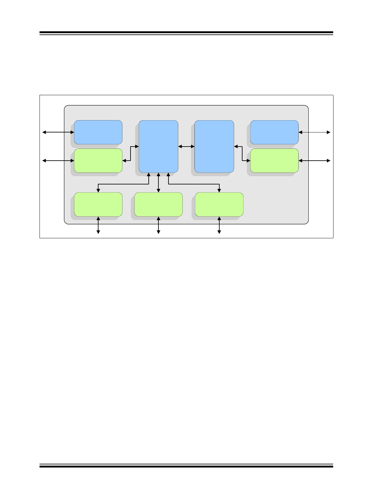
INTRODUCTION
1.1
Block Diagram
1.1.1
OVERVIEW
The LAN9513/LAN9513i is a high performance Hi-Speed USB 2.0 hub with a 10/100 Ethernet controller. With applica-
tions ranging from embedded systems, desktop PCs, notebook PCs, printers, game consoles, and docking stations, the
LAN9513/LAN9513i is targeted as a high performance, low cost USB/Ethernet and USB/USB connectivity solution.
The LAN9513/LAN9513i contains an integrated USB 2.0 hub, three integrated downstream USB 2.0 PHYs, an inte-
grated upstream USB 2.0 PHY, a 10/100 Ethernet PHY, a 10/100 Ethernet Controller, a TAP controller, and a EEPROM
controller. A block diagram of the LAN9513/LAN9513i is provided in
Figure 1-1
.
The LAN9513/LAN9513i hub provides over 30 programmable features, including:
• PortMap (also referred to as port remap) which provides flexible port mapping and disabling sequences. The
downstream ports of the LAN9513/LAN9513i hub can be reordered or disabled in any sequence to support multi-
ple platform designs’ with minimum effort. For any port that is disabled, the LAN9513/LAN9513i automatically
reorders the remaining ports to match the USB host controller’s port numbering scheme.
• PortSwap which adds per-port programmability to USB differential pair pin locations. PortSwap allows direct
alignment of USB signals (D+/D-) to connectors avoiding uneven trace length or crossing of the USB differential
signals on the PCB.
• PHYBoost which enables four programmable levels of USB signal drive strength in USB port transceivers. PHY-
Boost attempts to restore USB signal integrity that has been compromised by system level variables such as poor
PCB layout, long cables, etc.
1.1.2
USB HUB
The integrated USB hub is fully compliant with the USB 2.0 Specification and will attach to a USB host as a Full-Speed
Hub or as a Full-/High-Speed Hub. The hub supports Low-Speed, Full-Speed, and High-Speed (if operating as a High-
Speed hub) downstream devices on all of the enabled downstream ports.
A dedicated Transaction Translator (TT) is available for each downstream facing port. This architecture ensures maxi-
mum USB throughput for each connected device when operating with mixed-speed peripherals.
The hub works with an external USB power distributed switch device to control V
BUS
switching to downstream ports,
and to limit current and sense over-current conditions.
FIGURE 1-1:
INTERNAL BLOCK DIAGRAM
TAP
Controller
EEPROM
Controller
10/100
Ethernet
Controller
USB 2.0
Hub
LAN9513/LAN9513i
Ethernet
EEPROM
JTAG
USB
DP/DM
Downstream
USB PHY
Ethernet
PHY
Upstream
USB PHY
Downstream
USB PHY
Downstream
USB PHY
USB
DP/DM
USB
DP/DM
USB
DP/DM

2009-2016 Microchip Technology Inc.
DS00002305A-page 5
LAN9513/LAN9513I
All required resistors on the USB ports are integrated into the hub. This includes all series termination resistors on D+
and D- pins and all required pull-down and pull-up resistors on D+ and D- pins. The over-current sense inputs for the
downstream facing ports have internal pull-up resistors.
Three external ports are available for general USB device connectivity.
1.1.3
ETHERNET CONTROLLER
The 10/100 Ethernet controller provides an integrated Ethernet MAC and PHY which are fully IEEE 802.3 10BASE-T
and 802.3u 100BASE-TX compliant. The 10/100 Ethernet controller also supports numerous power management
wakeup features, including “Magic Packet”, “Wake on LAN” and “Link Status Change”. These wakeup events can be
programmed to initiate a USB remote wakeup.
The 10/100 Ethernet PHY integrates an IEEE 802.3 physical layer for twisted pair Ethernet applications. The PHY block
includes support for auto-negotiation, full or half-duplex configuration, auto-polarity correction and Auto-MDIX. Minimal
external components are required for the utilization of the integrated PHY.
The Ethernet controller implements four USB endpoints: Control, Interrupt, Bulk-in, and Bulk-out. The Bulk-in and Bulk-
out Endpoints allow for Ethernet reception and transmission respectively. Implementation of vendor-specific commands
allows for efficient statistics gathering and access to the Ethernet controller’s system control and status registers.
1.1.4
EEPROM CONTROLLER
The LAN9513/LAN9513i contains an EEPROM controller for connection to an external EEPROM. This allows for the
automatic loading of static configuration data upon power-on reset, pin reset, or software reset. The EEPROM can be
configured to load USB descriptors, USB device configuration, and the MAC address.
1.1.5
PERIPHERALS
The LAN9513/LAN9513i also contains a TAP controller, and provides three PHY LED indicators, as well as eight general
purpose I/O pins. All GPIOs can serve as remote wakeup events when LAN9513/LAN9513i is in a suspended state.
The integrated IEEE 1149.1 compliant TAP controller provides boundary scan via JTAG.
1.1.6
POWER MANAGEMENT
The LAN9513/LAN9513i features three variations of USB suspend: SUSPEND0, SUSPEND1, and SUSPEND2. These
modes allow the application to select the ideal balance of remote wakeup functionality and power consumption.
• SUSPEND0: Supports GPIO, “Wake On LAN”, and “Magic Packet” remote wakeup events. This suspend state
reduces power by stopping the clocks of the MAC and other internal modules.
• SUSPEND1: Supports GPIO and “Link Status Change” for remote wakeup events. This suspend state consumes
less power than SUSPEND0.
• SUSPEND2: Supports only GPIO assertion for a remote wakeup event. This is the default suspend mode for the
LAN9513/LAN9513i.
LAN9513/LAN9513I
DS00002305A-page 6
2009-2016 Microchip Technology Inc.
2.0
PIN DESCRIPTION AND CONFIGURATION
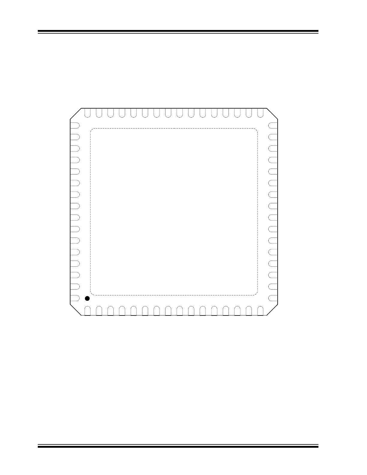
FIGURE 2-1:
LAN9513/LAN9513I 64-QFN PIN ASSIGNMENTS (TOP VIEW)
NOTE: Exposed pad (VSS) on bottom of package must be connected to ground
NOTE: When HP Auto-MDIX is activated, the TXN/TXP pins can function as RXN/RXP and vice-versa
EXRES
TE
ST
4
TDO
PRTC
TL
2
1
2
3
4
5
6
7
8
9
10
11
12
13
14
18
19
20
21
22
23
24
25
26
27
28
29
30
31
47
46
45
44
43
42
41
40
39
38
37
36
35
34
63
62
61
60
59
58
57
56
55
54
53
52
51
50
TE
ST
1
nR
ES
ET
VB
U
S_D
ET
VD
D33A
NC
NC
US
B
D
P4
USB
D
M4
VD
D33A
US
B
D
P3
USBDM3
US
B
D
P2
USBDM2
VDD33I
O
CLK24_O
U
T
CLK24_EN
GPIO
7
GPIO
6
AU
TO
M
D
IX
_E
N
TE
ST
3
VDD33I
O
VDD18C
OR
E
GPIO
5
GPIO
4
GPIO
3
TE
ST
2
VDD33A
RXP
RXN
VDD33A
TXP
TXN
VDD33A
USBDM0
USBDP0
XO
XI
VDD18USBPLL
USBRBIAS
TDI
TMS
nTRST
VDD33IO
EEDI
EEDO
EECS
EECLK
nSPD_LED/GPIO2
nLNKA_LED/GPIO1
nFDX_LED/GPIO0
VDD33IO
NC
VDD33A
49
VDD33A
64
33
VDD33I
O
48
VDD18E
TH
PL
L
32
TCK
17
PRTCTL4
VD
D
18CORE
15
PR
TC
TL
3
16
VSS
SMSC
LAN9513/LAN9513i
64 PIN QFN
(TOP VIEW)

2009-2016 Microchip Technology Inc.
DS00002305A-page 7
LAN9513/LAN9513I
TABLE 2-1:
EEPROM PINS
Num
PINs
Name
Symbol
Buffer
Type
Description
1
EEPROM Data
In
EEDI
IS
(PD)
This pin is driven by the EEDO output of the
external EEPROM.
1
EEPROM Data
Out
EEDO
O8
This pin drives the EEDI input of the external
EEPROM.
1
EEPROM Chip
Select
EECS
O8
This pin drives the chip select output of the external
EEPROM.
1
EEPROM Clock
EECLK
O8
This pin drives the EEPROM clock of the external
EEPROM.
TABLE 2-2:
JTAG PINS
Num
PINs
Name
Symbol
Buffer
Type
Description
1
JTAG Test Port
Reset
nTRST
IS
This active low pin functions as the JTAG test port
reset input.
Note:
This pin should be tied high if it is not
used.
1
JTAG Test
Mode Select
TMS
IS
This pin functions as the JTAG test mode select.
1
JTAG Test Data
Input
TDI
IS
This pin functions as the JTAG data input.
1
JTAG Test Data
Out
TDO
O12
This pin functions as the JTAG data output.
1
JTAG Test
Clock
TCK
IS
This pin functions as the JTAG test clock. This pin
should be tied high through a 10 kΩ resistor.

LAN9513/LAN9513I
DS00002305A-page 8
2009-2016 Microchip Technology Inc.
TABLE 2-3:
MISCELLANEOUS PINS
Num
PINs
Name
Symbol
Buffer
Type
Description
1
System Reset
nRESET
IS
This active low pin allows external hardware to
reset the device.
Note:
This pin should be tied high if it is not
used.
1
Ethernet
Full-Duplex Indi-
cator LED
nFDX_LED
OD12
(PU)
This pin is driven low (LED on) when the Ethernet
link is operating in full-duplex mode.
General Pur-
pose I/O 0
GPIO0
IS/O12/
OD12
(PU)
This General Purpose I/O pin is fully programmable
as either a push-pull output, an open-drain output,
or a Schmitt-triggered input.
1
Ethernet Link
Activity Indica-
tor LED
nLNKA_LED
OD12
(PU)
This pin is driven low (LED on) when a valid link is
detected. This pin is pulsed high (LED off) for
80 mS whenever transmit or receive activity is
detected. This pin is then driven low again for a
minimum of 80 mS, after which time it will repeat
the process if TX or RX activity is detected.
Effectively, LED2 is activated solid for a link. When
transmit or receive activity is sensed, LED2 will
function as an activity indicator.
General Pur-
pose I/O 1
GPIO1
IS/O12/
OD12
(PU)
This General Purpose I/O pin is fully programmable
as either a push-pull output, an open-drain output,
or a Schmitt-triggered input.
1
Ethernet Speed
Indicator LED
nSPD_LED
OD12
(PU)
This pin is driven low (LED on) when the Ethernet
operating speed is 100 Mbs, or during auto-
negotiation. This pin is driven high during 10Mbs
operation, or during line isolation.
General Pur-
pose I/O 2
GPIO2
IS/O12/
OD12
(PU)
This General Purpose I/O pin is fully programmable
as either a push-pull output, an open-drain output,
or a Schmitt-triggered input.
1
General Pur-
pose I/O 3
GPIO3
IS/O8/
OD8
(PU)
This General Purpose I/O pin is fully programmable
as either a push-pull output, an open-drain output,
or a Schmitt-triggered input.
1
General Pur-
pose I/O 4
GPIO4
IS/O8/
OD8
(PU)
This General Purpose I/O pin is fully programmable
as either a push-pull output, an open-drain output,
or a Schmitt-triggered input.
1
General Pur-
pose I/O 5
GPIO5
IS/O8/
OD8
(PU)
This General Purpose I/O pin is fully programmable
as either a push-pull output, an open-drain output,
or a Schmitt-triggered input.
1
General Pur-
pose I/O 6
GPIO6
IS/O8/
OD8
(PU)
This General Purpose I/O pin is fully programmable
as either a push-pull output, an open-drain output,
or a Schmitt-triggered input.
1
General Pur-
pose I/O 7
GPIO7
IS/O8/
OD8
(PU)
This General Purpose I/O pin is fully programmable
as either a push-pull output, an open-drain output,
or a Schmitt-triggered input.

2009-2016 Microchip Technology Inc.
DS00002305A-page 9
LAN9513/LAN9513I
1
Detect
Upstream VBUS
Power
VBUS_DET
IS_5V
This pin detects the state of the upstream bus
power. The Hub monitors VBUS_DET to determine
when to assert the USBDP0 pin's internal pull-up
resistor (signaling a connect event).
For bus-powered hubs, this pin must be tied to
VDD33IO.
For self-powered hubs where the device is
permanently attached to a host, VBUS_DET should
be pulled to VDD33IO. For other self-powered
applications, refer to the device reference
schematic for additional connection information.
1
Auto-MDIX
Enable
AUTOMDIX_EN
IS
Determines the default Auto-MDIX setting.
0 = Auto-MDIX is disabled.
1 = Auto-MDIX is enabled.
1
Test 1
TEST1
—
Used for factory testing, this pin must always be left
unconnected.
1
Test 2
TEST2
—
Used for factory testing, this pin must always be
connected to VSS for proper operation.
1
Test 3
TEST3
—
Used for factory testing, this pin must always be
connected to VDD33IO for proper operation.
1
24 MHz Clock
Enable
CLK24_EN
IS
This pin enables the generation of the 24 MHz
clock on the CLK_24_OUT pin.
1
24 MHz Clock
CLK24_OUT
08
This pin outputs a 24 MHz clock that can be used
a reference clock for a partner hub.
1
Test 4
TEST4
—
Used for factory testing, this pin must always be left
unconnected.
TABLE 2-4:
USB PINS
Num
PINs
Name
Symbol
Buffer
Type
Description
1
Upstream
USB DMINUS 0
USBDM0
AIO
Upstream USB DMINUS signal.
1
Upstream
USB
DPLUS 0
USBDP0
AIO
Upstream USB DPLUS signal.
1
Downstream
USB DMINUS 2
USBDM2
AIO
Downstream USB peripheral 2 DMINUS signal.
1
Downstream
USB DPLUS 2
USBDP2
AIO
Downstream USB peripheral 2 DPLUS signal.
TABLE 2-3:
MISCELLANEOUS PINS (CONTINUED)
Num
PINs
Name
Symbol
Buffer
Type
Description

LAN9513/LAN9513I
DS00002305A-page 10
2009-2016 Microchip Technology Inc.
1
Downstream
USB DMINUS 3
USBDM3
AIO
Downstream USB peripheral 3 DMINUS signal.
1
Downstream
USB DPLUS 3
USBDP3
AIO
Downstream USB peripheral 3 DPLUS signal.
1
Downstream
USB DMINUS 4
USBDM4
AIO
Downstream USB peripheral 4 DMINUS signal.
1
Downstream
USB DPLUS 4
USBDP4
AIO
Downstream USB peripheral 4 DPLUS signal.
1
USB Port Power
Control 2
PRTCTL2
IS/OD12
(PU)
When used as an output, this pin enables power to
downstream USB peripheral 2.
When used as an input, this pin is used to sample
the output signal from an external current monitor
for downstream USB peripheral 2. An overcurrent
condition is indicated when the signal is low.
Refer to
Section 2.2
for additional information.
1
USB Port Power
Control 3
PRTCTL3
IS/OD12
(PU)
When used as an output, this pin enables power to
downstream USB peripheral 3.
When used as an input, this pin is used to sample
the output signal from an external current monitor
for downstream USB peripheral 3. An overcurrent
condition is indicated when the signal is low.
Refer to
Section 2.2
for additional information.
1
USB Port Power
Control 4
PRTCTL4
IS/OD12
(PU)
When used as an output, this pin enables power to
downstream USB peripheral 4.
When used as an input, this pin is used to sample
the output signal from an external current monitor
for downstream USB peripheral 4. An overcurrent
condition is indicated when the signal is low.
Refer to
Section 2.2
for additional information.
1
External USB
Bias Resistor
USBRBIAS
AI
Used for setting HS transmit current level and on-
chip termination impedance. Connect to an
external 12K 1.0% resistor to ground.
1
USB PLL +1.8V
Power Supply
VDD18USBPLL
P
Refer to the LAN9513/LAN9513i reference
schematics for additional connection information.
1
Crystal Input
XI
ICLK
External 25 MHz crystal input.
Note:
This pin can also be driven by a single-
ended clock oscillator. When this method
is used, XO should be left unconnected
1
Crystal Output
XO
OCLK
External 25 MHz crystal output.
TABLE 2-4:
USB PINS (CONTINUED)
Num
PINs
Name
Symbol
Buffer
Type
Description