

2015 Microchip Technology Inc.
DS00001926B-page 1
Highlights
• High performance 3-port switch with VLAN, QoS
packet prioritization, rate limiting, IGMP monitoring
and management functions
• Integrated Ethernet PHYs with HP Auto-MDIX
• Compliant with Energy Efficient Ethernet 802.3az
• Wake on LAN (WoL) support
• Integrated IEEE 1588v2 hardware time stamp unit
• Cable diagnostic support
• 1.8V to 3.3V variable voltage I/O
• Integrated 1.2V regulator for single 3.3V operation
Target Applications
• Cable, satellite, and IP set-top boxes
• Digital televisions & video recorders
• VoIP/Video phone systems, home gateways
• Test/Measurement equipment, industrial automation
Key Benefits
• Ethernet Switch Fabric
- 32K buffer RAM, 512 entry forwarding table
- Port based IEEE 802.1Q VLAN support (16 groups)
- Programmable IEEE 802.1Q tag insertion/removal
- IEEE 802.1D spanning tree protocol support
- 4 separate transmit queues available per port
- Fixed or weighted egress priority servicing
- QoS/CoS Packet prioritization
- Input priority determined by VLAN tag, DA lookup, TOS,
DIFFSERV or port default value
- Programmable Traffic Class map based on input priority
on per port basis
- Remapping of 802.1Q priority field on per port basis
- Programmable rate limiting at the ingress with coloring
and random early discard, per port / priority
- Programmable rate limiting at the egress with leaky
bucket algorithm, per port / priority
- IGMP v1/v2/v3 monitoring for Multicast packet filtering
- Programmable broadcast storm protection with global %
control and enable per port
- Programmable buffer usage limits
- Dynamic queues on internal memory
- Programmable filter by MAC address
• Switch Management
- Port mirroring/monitoring/sniffing: ingress and/or egress
traffic on any port or port pair
- Fully compliant statistics (MIB) gathering counters
• Ports
- Port 0: RMII PHY, RMII MAC modes
- Port 1: Internal PHY
- Port 2: Internal PHY
- 2 internal 10/100 PHYs with HP Auto-MDIX
support
- Fully compliant with IEEE 802.3 standards
- 10BASE-T and 100BASE-TX support
- 100BASE-FX support via external fiber transceiver
- Full and half duplex support, full duplex flow control
- Backpressure (forced collision) half duplex flow control
- Automatic flow control based on programmable levels
- Automatic 32-bit CRC generation and checking
- Programmable interframe gap, flow control pause value
- Auto-negotiation, polarity correction & MDI/MDI-X
• IEEE 1588v2 hardware time stamp unit
- Global 64-bit tunable clock
- Boundary clock: master / slave, one-step / two-step,
end-to-end / peer-to-peer delay
- Transparent Clock with Ordinary Clock:
master / slave, one-step / two-step, end-to-end / peer-
to-peer delay
- Fully programmable timestamp on TX or RX,
timestamp on GPIO
- 64-bit timer comparator event generation (GPIO or IRQ)
• Comprehensive power management features
- 3 power-down levels
- Wake on link status change (energy detect)
- Magic packet wakeup, Wake on LAN (WoL), wake on
broadcast, wake on perfect DA
- Wakeup indicator event signal
• Power and I/O
- Integrated power-on reset circuit
- Latch-up performance exceeds 150mA
per EIA/JESD78, Class II
- JEDEC Class 3A ESD performance
- Single 3.3V power supply
(integrated 1.2V regulator)
• Additional Features
- Multifunction GPIOs
- Ability to use low cost 25MHz crystal for reduced BOM
• Packaging
- Pb-free RoHS compliant 56-pin QFN
• Available in commercial and industrial temp. ranges
LAN9354
3-Port 10/100 Managed Ethernet Switch with
Single RMII

LAN9354
DS00001926B-page 2
2015 Microchip Technology Inc.
TO OUR VALUED CUSTOMERS
It is our intention to provide our valued customers with the best documentation possible to ensure successful use of your Microchip
products. To this end, we will continue to improve our publications to better suit your needs. Our publications will be refined and
enhanced as new volumes and updates are introduced.
If you have any questions or comments regarding this publication, please contact the Marketing Communications Department via
E-mail at
docerrors@microchip.com
. We welcome your feedback.
Most Current Documentation
To obtain the most up-to-date version of this documentation, please register at our Worldwide Web site at:
http://www.microchip.com
You can determine the version of a data sheet by examining its literature number found on the bottom outside corner of any page.
The last character of the literature number is the version number, (e.g., DS30000000A is version A of document DS30000000).
Errata
An errata sheet, describing minor operational differences from the data sheet and recommended workarounds, may exist for cur-
rent devices. As device/documentation issues become known to us, we will publish an errata sheet. The errata will specify the
revision of silicon and revision of document to which it applies.
To determine if an errata sheet exists for a particular device, please check with one of the following:
• Microchip’s Worldwide Web site;
http://www.microchip.com
• Your local Microchip sales office (see last page)
When contacting a sales office, please specify which device, revision of silicon and data sheet (include -literature number) you are
using.
Customer Notification System
Register on our web site at
www.microchip.com
to receive the most current information on all of our products.

2015 Microchip Technology Inc.
DS00001926B-page 3
LAN9354
1.0 Preface ............................................................................................................................................................................................ 4
2.0 General Description ........................................................................................................................................................................ 8
3.0 Pin Descriptions and Configuration ............................................................................................................................................... 10
4.0 Power Connections ....................................................................................................................................................................... 26
5.0 Register Map ................................................................................................................................................................................. 29
6.0 Clocks, Resets, and Power Management ..................................................................................................................................... 37
7.0 Configuration Straps ..................................................................................................................................................................... 54
8.0 System Interrupts .......................................................................................................................................................................... 67
9.0 Ethernet PHYs .............................................................................................................................................................................. 77
10.0 Switch Fabric ............................................................................................................................................................................ 182
11.0 I2C Slave Controller .................................................................................................................................................................. 319
12.0 I2C Master EEPROM Controller ............................................................................................................................................... 324
13.0 MII Data Interfaces .................................................................................................................................................................... 340
14.0 MII Management ....................................................................................................................................................................... 346
15.0 IEEE 1588 ................................................................................................................................................................................. 361
16.0 General Purpose Timer & Free-Running Clock ........................................................................................................................ 447
17.0 GPIO/LED Controller ................................................................................................................................................................ 451
18.0 Miscellaneous ........................................................................................................................................................................... 460
19.0 JTAG ......................................................................................................................................................................................... 465
20.0 Operational Characteristics ....................................................................................................................................................... 467
21.0 Package Outlines ...................................................................................................................................................................... 481
22.0 Revision History ........................................................................................................................................................................ 483

LAN9354
DS00001926B-page 4
2015 Microchip Technology Inc.
1.0
PREFACE
1.1
General Terms
TABLE 1-1:
GENERAL TERMS
Term
Description
10BASE-T
10 Mbps Ethernet, IEEE 802.3 compliant
100BASE-TX
100 Mbps Fast Ethernet, IEEE802.3u compliant
ADC
Analog-to-Digital Converter
ALR
Address Logic Resolution
AN
Auto-Negotiation
BLW
Baseline Wander
BM
Buffer Manager - Part of the switch fabric
BPDU
Bridge Protocol Data Unit - Messages which carry the Spanning Tree Protocol informa-
tion
Byte
8 bits
CSMA/CD
Carrier Sense Multiple Access/Collision Detect
CSR
Control and Status Registers
CTR
Counter
DA
Destination Address
DWORD
32 bits
EPC
EEPROM Controller
FCS
Frame Check Sequence - The extra checksum characters added to the end of an
Ethernet frame, used for error detection and correction.
FIFO
First In First Out buffer
FSM
Finite State Machine
GPIO
General Purpose I/O
Host
External system (Includes processor, application software, etc.)
IGMP
Internet Group Management Protocol
Inbound
Refers to data input to the device from the host
Level-Triggered Sticky Bit
This type of status bit is set whenever the condition that it represents is asserted. The
bit remains set until the condition is no longer true and the status bit is cleared by writ-
ing a zero.
lsb
Least Significant Bit
LSB
Least Significant Byte
LVDS
Low Voltage Differential Signaling
MDI
Medium Dependent Interface
MDIX
Media Independent Interface with Crossover
MII
Media Independent Interface
MIIM
Media Independent Interface Management
MIL
MAC Interface Layer
MLD
Multicast Listening Discovery
MLT-3
Multi-Level Transmission Encoding (3-Levels). A tri-level encoding method where a
change in the logic level represents a code bit “1” and the logic output remaining at the
same level represents a code bit “0”.
msb
Most Significant Bit
MSB
Most Significant Byte

2015 Microchip Technology Inc.
DS00001926B-page 5
LAN9354
NRZI
Non Return to Zero Inverted. This encoding method inverts the signal for a “1” and
leaves the signal unchanged for a “0”
N/A
Not Applicable
NC
No Connect
OUI
Organizationally Unique Identifier
Outbound
Refers to data output from the device to the host
PISO
Parallel In Serial Out
PLL
Phase Locked Loop
PTP
Precision Time Protocol
RESERVED
Refers to a reserved bit field or address. Unless otherwise noted, reserved bits must
always be zero for write operations. Unless otherwise noted, values are not guaran-
teed when reading reserved bits. Unless otherwise noted, do not read or write to
reserved addresses.
RTC
Real-Time Clock
SA
Source Address
SFD
Start of Frame Delimiter - The 8-bit value indicating the end of the preamble of an
Ethernet frame.
SIPO
Serial In Parallel Out
SMI
Serial Management Interface
SQE
Signal Quality Error (also known as “heartbeat”)
SSD
Start of Stream Delimiter
UDP
User Datagram Protocol - A connectionless protocol run on top of IP networks
UUID
Universally Unique IDentifier
WORD
16 bits
TABLE 1-1:
GENERAL TERMS (CONTINUED)
Term
Description

LAN9354
DS00001926B-page 6
2015 Microchip Technology Inc.
1.2
Buffer Types
TABLE 1-2:
BUFFER TYPES
Buffer Type
Description
IS
Schmitt-triggered input
VIS
Variable voltage Schmitt-triggered input
VO8
Variable voltage output with 8 mA sink and 8 mA source
VOD8
Variable voltage open-drain output with 8 mA sink
VO12
Variable voltage output with 12 mA sink and 12 mA source
VOD12
Variable voltage open-drain output with 12 mA sink
VOS12
Variable voltage open-source output with 12 mA source
VO16
Variable voltage output with 16 mA sink and 16 mA source
PU
50 µA (typical) internal pull-up. Unless otherwise noted in the pin description, internal pull-
ups are always enabled.
Internal pull-up resistors prevent unconnected inputs from floating. Do not rely on internal
resistors to drive signals external to the device. When connected to a load that must be
pulled high, an external resistor must be added.
PD
50 µA (typical) internal pull-down. Unless otherwise noted in the pin description, internal
pull-downs are always enabled.
Internal pull-down resistors prevent unconnected inputs from floating. Do not rely on internal
resistors to drive signals external to the device. When connected to a load that must be
pulled low, an external resistor must be added.
AI
Analog input
AIO
Analog bidirectional
ICLK
Crystal oscillator input pin
OCLK
Crystal oscillator output pin
ILVPECL
Low voltage PECL input pin
OLVPECL
Low voltage PECL output pin
P
Power pin

2015 Microchip Technology Inc.
DS00001926B-page 7
LAN9354
1.3
Register Nomenclature
TABLE 1-3:
REGISTER NOMENCLATURE
Register Bit Type Notation
Register Bit Description
R
Read:
A register or bit with this attribute can be read.
W
Read:
A register or bit with this attribute can be written.
RO
Read only:
Read only. Writes have no effect.
WO
Write only:
If a register or bit is write-only, reads will return unspecified data.
WC
Write One to Clear:
Writing a one clears the value. Writing a zero has no effect
WAC
Write Anything to Clear:
Writing anything clears the value.
RC
Read to Clear:
Contents is cleared after the read. Writes have no effect.
LL
Latch Low:
Clear on read of register.
LH
Latch High:
Clear on read of register.
SC
Self-Clearing:
Contents are self-cleared after the being set. Writes of zero have no
effect. Contents can be read.
SS
Self-Setting:
Contents are self-setting after being cleared. Writes of one have no
effect. Contents can be read.
RO/LH
Read Only, Latch High:
Bits with this attribute will stay high until the bit is read. After it
is read, the bit will either remain high if the high condition remains, or will go low if the
high condition has been removed. If the bit has not been read, the bit will remain high
regardless of a change to the high condition. This mode is used in some Ethernet PHY
registers.
NASR
Not Affected by Software Reset.
The state of NASR bits do not change on assertion
of a software reset.
RESERVED
Reserved Field:
Reserved fields must be written with zeros to ensure future compati-
bility. The value of reserved bits is not guaranteed on a read.

LAN9354
DS00001926B-page 8
2015 Microchip Technology Inc.
2.0
GENERAL DESCRIPTION
The LAN9354 is a full featured, 3 port 10/100 managed Ethernet switch designed for embedded applications where per-
formance, flexibility, ease of integration and system cost control are required. The LAN9354 combines all the functions
of a 10/100 switch system, including the Switch Fabric, packet buffers, Buffer Manager, Media Access Controllers
(MACs), PHY transceivers, and serial management. IEEE 1588v2 is supported via the integrated IEEE 1588v2 hard-
ware time stamp unit, which supports end-to-end and peer-to-peer transparent clocks. The LAN9354 complies with the
IEEE 802.3 (full/half-duplex 10BASE-T and 100BASE-TX) Ethernet protocol, IEEE 802.3az Energy Efficient Ethernet
(EEE) (100Mbps only), and 802.1D/802.1Q network management protocol specifications, enabling compatibility with
industry standard Ethernet and Fast Ethernet applications. 100BASE-FX is supported via an external fiber transceiver.
At the core of the device is the high performance, high efficiency 3 port Ethernet Switch Fabric. The Switch Fabric con-
tains a 3 port VLAN layer 2 Switch Engine that supports untagged, VLAN tagged, and priority tagged frames. The Switch
Fabric provides an extensive feature set which includes spanning tree protocol support, multicast packet filtering and
Quality of Service (QoS) packet prioritization by VLAN tag, destination address, port default value or DIFFSERV/TOS,
allowing for a range of prioritization implementations. 32K of buffer RAM allows for the storage of multiple packets while
forwarding operations are completed, and a 512 entry forwarding table provides ample room for MAC address forward-
ing tables. Each port is allocated a cluster of 4 dynamic QoS queues which allow each queue size to grow and shrink
with traffic, effectively utilizing all available memory. This memory is managed dynamically via the Buffer Manager block
within the Switch Fabric. All aspects of the Switch Fabric are managed via the Switch Fabric configuration and status
registers, which are indirectly accessible via the system control and status registers.
The LAN9354 provides 3 switched ports. Each port is fully compliant with the IEEE 802.3 standard and all internal MACs
and PHYs support full/half duplex 10BASE-T and 100BASE-TX operation. The LAN9354 provides 2 on-chip PHYs, 1
Virtual PHY and 3 MACs. The Virtual PHY and the third MAC are used to connect the Switch Fabric to an external MAC
or PHY. In MAC mode, the device can be connected to an external PHY via the RMII interface. In PHY mode, the device
can be connected to an external MAC via the RMII interface. All ports support automatic or manual full duplex flow con-
trol or half duplex backpressure (forced collision) flow control. 2K jumbo packet (2048 byte) support allows for oversized
packet transfers, effectively increasing throughput while decreasing CPU load. All MAC and PHY related settings are
fully configurable via their respective registers within the device.
The integrated I
2
C and SMI slave controllers allow for full serial management of the device via the integrated I
2
C or RMII
interface, respectively. The inclusion of these interfaces allows for greater flexibility in the incorporation of the device
into various designs. It is this flexibility which allows the device to operate in 2 different modes and under various man-
agement conditions. In both MAC and PHY modes, the device can be SMI managed or I
2
C managed. This flexibility in
management makes the LAN9354 a candidate for virtually all switch applications.
The LAN9354 supports numerous power management and wakeup features. The LAN9354 can be placed in a reduced
power mode and can be programmed to issue an external wake signal (IRQ) via several methods, including “Magic
Packet”, “Wake on LAN”, wake on broadcast, wake on perfect DA, and “Link Status Change”. This signal is ideal for
triggering system power-up using remote Ethernet wakeup events. The device can be removed from the low power state
via a host processor command or one of the wake events.
The LAN9354 contains an I
2
C master EEPROM controller for connection to an optional EEPROM. This allows for the
storage and retrieval of static data. The internal EEPROM Loader can be optionally configured to automatically load
stored configuration settings from the EEPROM into the device at reset. The I
2
C management slave and master
EEPROM controller share common pins.
In addition to the primary functionality described above, the LAN9354 provides additional features designed for
extended functionality. These include a configurable 16-bit General Purpose Timer (GPT), a 32-bit 25MHz free running
counter, a configurable GPIO/LED interface, and IEEE 1588 time stamping on all ports and all GPIOs. The IEEE time
stamp unit provides a 64-bit tunable clock for accurate PTP timing and a timer comparator to allow time based interrupt
generation.
The LAN9354 can be configured to operate via a single 3.3V supply utilizing an integrated 3.3V to 1.2V linear regulator.
The linear regulator may be optionally disabled, allowing usage of a high efficiency external regulator for lower system
power dissipation.
The LAN9354 is available in commercial and industrial temperature ranges.
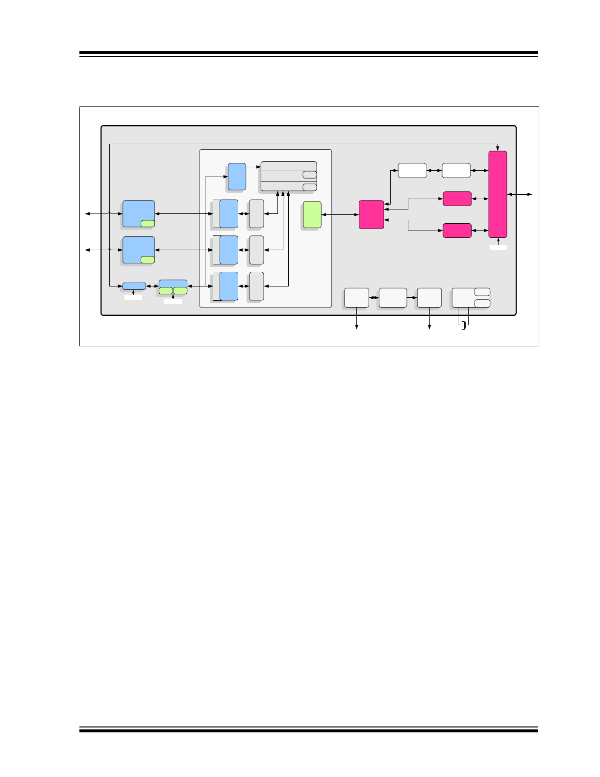
Figure 2-1
provides an internal block dia-
gram of the LAN9354.
2015 Microchip Technology Inc.
DS00001926B-page 9
LAN9354
FIGURE 2-1:
INTERNAL BLOCK DIAGRAM
LAN9354
RMII
Registers
Virtual PHY
MAC to
MAC
Switch
Registers
(CSRs)
Switch Fabric
Dyna
m
ic Qo
S
4 Q
u
eu
es
Po
rt
2
10/100
MAC
w/
802.3az
Dynam
ic Qo
S
4 Q
ueu
es
Po
rt 1
10/100
MAC
w/
802.3az
Dynam
ic
Q
o
S
4 Que
ues
Po
rt 0
10/100
MAC
w/
802.3az
Switch Engine
Buffer Manager
Search
Engine
Frame
Buffers
1588 Transparent Clocking
IEEE
1588v2
Time
Stamp
GPIO/LED
Controller
To optional GPIOs/LEDs
System
Interrupt
Controller
IRQ
GP Timer
Free-Run
Clk
System
Clocks/
Reset/PME
Controller
External
25MHz Crystal
IEEE 1588v2
Clock/Events
Configuration
Register
Access
Mux
I
2
C Slave
I
2
C
EEPROM
Configuration
10/100 PHY
w/fiber
w/802.3az
Registers
Ethernet
EEPROM
Loader
SMI Slave
Controller
PIN
Mux
Configuration
10/100 PHY
w/fiber
w/802.3az
Registers
Ethernet
To RMII,
SMI, I2C
LAN9354
DS00001926B-page 10
2015 Microchip Technology Inc.
3.0
PIN DESCRIPTIONS AND CONFIGURATION
3.1
56-QFN Pin Assignments
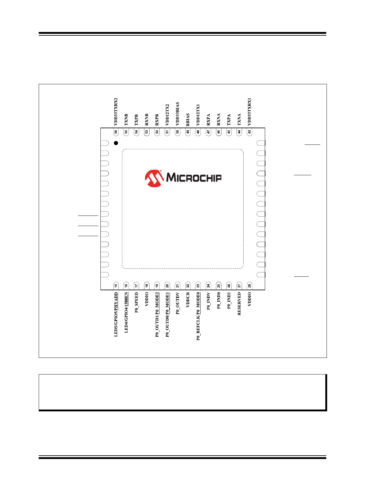
FIGURE 3-1:
56-QFN PIN ASSIGNMENTS (TOP VIEW)
Note:
When a “#” is used at the end of the signal name, it indicates that the signal is active low. For example,
RST# indicates that the reset signal is active low.
The buffer type for each signal is indicated in the “Buffer Type” column of the pin description tables in
Sec-
tion 3.2, "Pin Descriptions"
. A description of the buffer types is provided in
Section 1.2, "Buffer Types"
.
Note: Exposed pad (VSS) on bottom of package must be connected to ground with a via field.
(Connect exposed pad to ground with a via field)
V SS
LAN9354
56-QFN
( T o p V i e w )
4
5
6
7
8
9
10
11
39
38
37
36
35
34
33
32
REG_EN
VDDCR
FXLOSEN
FXSDA/FXLOSA/FXSDENA
FXSDB/FXLOSB/FXSDENB
RST#
GPIO7
GPIO6
VDDIO
LED1/GPIO1/TDI
IRQ
P0_MDC
VDDIO
P0_DUPLEX
I2CSCL/EESCL/TCK
LED2/GPIO2/E2PSIZE
2
3
12
13
31
30
41
40
VDD33
OSCVSS
OSCVDD12
OSCO
I2CSDA/EESDA/TMS
TESTMODE
P0_MDIO
VDDCR
1
OSCI
14
VDDIO
29
LED3/GPIO3/EEEEN
LED0/GPIO0/TDO/MNGT0
42