

2015 Microchip Technology Inc.
DS00001909A-page 1
Highlights
• 2/3-port EtherCAT slave controller with 3 Fieldbus
Memory Management Units (FMMUs) and
4 SyncManagers
• Interfaces to most 8/16-bit embedded controllers
and 32-bit embedded controllers with an 8/16-bit
bus
• Integrated Ethernet PHYs with HP Auto-MDIX
• Wake on LAN (WoL) support
• Low power mode allows systems to enter sleep
mode until addressed by the Master
• Cable diagnostic support
• 1.8V to 3.3V variable voltage I/O
• Integrated 1.2V regulator for single 3.3V operation
• Low pin count and small body size package
Target Applications
• Motor Motion Control
• Process/Factory Automation
• Communication Modules, Interface Cards
• Sensors
• Hydraulic & Pneumatic Valve Systems
• Operator Interfaces
Key Benefits
• Integrated high-performance 100Mbps Ethernet
transceivers
- Compliant with IEEE 802.3/802.3u (Fast Ethernet)
- 100BASE-FX support via external fiber transceiver
- Loop-back modes
- Automatic polarity detection and correction
- HP Auto-MDIX
• EtherCAT slave controller
- Supports 3 FMMUs
- Supports 4 SyncManagers
- Distributed clock support allows synchronization with
other EtherCAT devices
- 4K bytes of DPRAM
• 8/16-Bit Host Bus Interface
- Indexed register or multiplexed bus
- Allows local host to enter sleep mode until addressed by
EtherCAT Master
- SPI / Quad SPI support
• Digital I/O Mode for optimized system cost
• 3rd port for flexible network configurations
• Comprehensive power management features
- 3 power-down levels
- Wake on link status change (energy detect)
- Magic packet wakeup, Wake on LAN (WoL), wake on
broadcast, wake on perfect DA
- Wakeup indicator event signal
• Power and I/O
- Integrated power-on reset circuit
- Latch-up performance exceeds 150mA
per EIA/JESD78, Class II
- JEDEC Class 3A ESD performance
- Single 3.3V power supply
(integrated 1.2V regulator)
• Additional Features
- Multifunction GPIOs
- Ability to use low cost 25MHz crystal for reduced BOM
• Packaging
- Pb-free RoHS compliant 64-pin QFN or 64-pin TQFP-
EP
• Available in commercial, industrial, and extended
industrial* temp. ranges
*Extended temp. (105ºC) is supported only in the 64-QFN with an
external voltage regulator (internal regulator must be disabled) and
2.5V (typ) Ethernet magnetics.
LAN9252
2/3-Port EtherCAT® Slave Controller with
Integrated Ethernet PHYs

LAN9252
DS00001909A-page 2
2015 Microchip Technology Inc.
TO OUR VALUED CUSTOMERS
It is our intention to provide our valued customers with the best documentation possible to ensure successful use of your Microchip
products. To this end, we will continue to improve our publications to better suit your needs. Our publications will be refined and
enhanced as new volumes and updates are introduced.
If you have any questions or comments regarding this publication, please contact the Marketing Communications Department via
E-mail at
docerrors@microchip.com
. We welcome your feedback.
Most Current Documentation
To obtain the most up-to-date version of this documentation, please register at our Worldwide Web site at:
http://www.microchip.com
You can determine the version of a data sheet by examining its literature number found on the bottom outside corner of any page.
The last character of the literature number is the version number, (e.g., DS30000000A is version A of document DS30000000).
Errata
An errata sheet, describing minor operational differences from the data sheet and recommended workarounds, may exist for cur-
rent devices. As device/documentation issues become known to us, we will publish an errata sheet. The errata will specify the
revision of silicon and revision of document to which it applies.
To determine if an errata sheet exists for a particular device, please check with one of the following:
• Microchip’s Worldwide Web site;
http://www.microchip.com
• Your local Microchip sales office (see last page)
When contacting a sales office, please specify which device, revision of silicon and data sheet (include -literature number) you are
using.
Customer Notification System
Register on our web site at
www.microchip.com
to receive the most current information on all of our products.

2015 Microchip Technology Inc.
DS00001909A-page 3
LAN9252
1.0 Preface ............................................................................................................................................................................................ 4
2.0 General Description ........................................................................................................................................................................ 8
3.0 Pin Descriptions and Configuration ............................................................................................................................................... 11
4.0 Power Connections ....................................................................................................................................................................... 29
5.0 Register Map ................................................................................................................................................................................. 32
6.0 Clocks, Resets, and Power Management ..................................................................................................................................... 37
7.0 Configuration Straps ..................................................................................................................................................................... 51
8.0 System Interrupts .......................................................................................................................................................................... 53
9.0 Host Bus Interface ........................................................................................................................................................................ 62
10.0 SPI/SQI Slave ........................................................................................................................................................................... 102
11.0 Ethernet PHYs .......................................................................................................................................................................... 120
12.0 EtherCAT .................................................................................................................................................................................. 196
13.0 EEPROM Interface ................................................................................................................................................................... 295
14.0 Chip Mode Configuration .......................................................................................................................................................... 296
15.0 General Purpose Timer & Free-Running Clock ........................................................................................................................ 297
16.0 Miscellaneous ........................................................................................................................................................................... 301
17.0 JTAG ......................................................................................................................................................................................... 305
18.0 Operational Characteristics ....................................................................................................................................................... 307
19.0 Package Outlines ...................................................................................................................................................................... 322
20.0 Revision History ........................................................................................................................................................................ 325

LAN9252
DS00001909A-page 4
2015 Microchip Technology Inc.
1.0
PREFACE
1.1
General Terms
TABLE 1-1:
GENERAL TERMS
Term
Description
10BASE-T
10 Mbps Ethernet, IEEE 802.3 compliant
100BASE-TX
100 Mbps Fast Ethernet, IEEE802.3u compliant
ADC
Analog-to-Digital Converter
ALR
Address Logic Resolution
AN
Auto-Negotiation
BLW
Baseline Wander
BM
Buffer Manager - Part of the switch fabric
BPDU
Bridge Protocol Data Unit - Messages which carry the Spanning Tree Protocol informa-
tion
Byte
8 bits
CSMA/CD
Carrier Sense Multiple Access/Collision Detect
CSR
Control and Status Registers
CTR
Counter
DA
Destination Address
DWORD
32 bits
EPC
EEPROM Controller
FCS
Frame Check Sequence - The extra checksum characters added to the end of an
Ethernet frame, used for error detection and correction.
FIFO
First In First Out buffer
FSM
Finite State Machine
GPIO
General Purpose I/O
Host
External system (Includes processor, application software, etc.)
IGMP
Internet Group Management Protocol
Inbound
Refers to data input to the device from the host
Level-Triggered Sticky Bit
This type of status bit is set whenever the condition that it represents is asserted. The
bit remains set until the condition is no longer true and the status bit is cleared by writ-
ing a zero.
lsb
Least Significant Bit
LSB
Least Significant Byte
LVDS
Low Voltage Differential Signaling
MDI
Medium Dependent Interface
MDIX
Media Independent Interface with Crossover
MII
Media Independent Interface
MIIM
Media Independent Interface Management
MIL
MAC Interface Layer
MLD
Multicast Listening Discovery
MLT-3
Multi-Level Transmission Encoding (3-Levels). A tri-level encoding method where a
change in the logic level represents a code bit “1” and the logic output remaining at the
same level represents a code bit “0”.
msb
Most Significant Bit
MSB
Most Significant Byte

2015 Microchip Technology Inc.
DS00001909A-page 5
LAN9252
NRZI
Non Return to Zero Inverted. This encoding method inverts the signal for a “1” and
leaves the signal unchanged for a “0”
N/A
Not Applicable
NC
No Connect
OUI
Organizationally Unique Identifier
Outbound
Refers to data output from the device to the host
PISO
Parallel In Serial Out
PLL
Phase Locked Loop
PTP
Precision Time Protocol
RESERVED
Refers to a reserved bit field or address. Unless otherwise noted, reserved bits must
always be zero for write operations. Unless otherwise noted, values are not guaran-
teed when reading reserved bits. Unless otherwise noted, do not read or write to
reserved addresses.
RTC
Real-Time Clock
SA
Source Address
SFD
Start of Frame Delimiter - The 8-bit value indicating the end of the preamble of an
Ethernet frame.
SIPO
Serial In Parallel Out
SMI
Serial Management Interface
SQE
Signal Quality Error (also known as “heartbeat”)
SSD
Start of Stream Delimiter
UDP
User Datagram Protocol - A connectionless protocol run on top of IP networks
UUID
Universally Unique IDentifier
WORD
16 bits
TABLE 1-1:
GENERAL TERMS (CONTINUED)
Term
Description

LAN9252
DS00001909A-page 6
2015 Microchip Technology Inc.
1.2
Buffer Types
TABLE 1-2:
BUFFER TYPES
Buffer Type
Description
IS
Schmitt-triggered input
VIS
Variable voltage Schmitt-triggered input
VO8
Variable voltage output with 8 mA sink and 8 mA source
VOD8
Variable voltage open-drain output with 8 mA sink
VO12
Variable voltage output with 12 mA sink and 12 mA source
VOD12
Variable voltage open-drain output with 12 mA sink
VOS12
Variable voltage open-source output with 12 mA source
VO16
Variable voltage output with 16 mA sink and 16 mA source
PU
50 µA (typical) internal pull-up. Unless otherwise noted in the pin description, internal pull-
ups are always enabled.
Internal pull-up resistors prevent unconnected inputs from floating. Do not rely on internal
resistors to drive signals external to the device. When connected to a load that must be
pulled high, an external resistor must be added.
PD
50 µA (typical) internal pull-down. Unless otherwise noted in the pin description, internal
pull-downs are always enabled.
Internal pull-down resistors prevent unconnected inputs from floating. Do not rely on internal
resistors to drive signals external to the device. When connected to a load that must be
pulled low, an external resistor must be added.
AI
Analog input
AIO
Analog bidirectional
ICLK
Crystal oscillator input pin
OCLK
Crystal oscillator output pin
ILVPECL
Low voltage PECL input pin
OLVPECL
Low voltage PECL output pin
P
Power pin

2015 Microchip Technology Inc.
DS00001909A-page 7
LAN9252
1.3
Register Nomenclature
TABLE 1-3:
REGISTER NOMENCLATURE
Register Bit Type Notation
Register Bit Description
R
Read:
A register or bit with this attribute can be read.
W
Read:
A register or bit with this attribute can be written.
RO
Read only:
Read only. Writes have no effect.
WO
Write only:
If a register or bit is write-only, reads will return unspecified data.
WC
Write One to Clear:
Writing a one clears the value. Writing a zero has no effect
WAC
Write Anything to Clear:
Writing anything clears the value.
RC
Read to Clear:
Contents is cleared after the read. Writes have no effect.
LL
Latch Low:
Clear on read of register.
LH
Latch High:
Clear on read of register.
SC
Self-Clearing:
Contents are self-cleared after the being set. Writes of zero have no
effect. Contents can be read.
SS
Self-Setting:
Contents are self-setting after being cleared. Writes of one have no
effect. Contents can be read.
RO/LH
Read Only, Latch High:
Bits with this attribute will stay high until the bit is read. After it
is read, the bit will either remain high if the high condition remains, or will go low if the
high condition has been removed. If the bit has not been read, the bit will remain high
regardless of a change to the high condition. This mode is used in some Ethernet PHY
registers.
NASR
Not Affected by Software Reset.
The state of NASR bits do not change on assertion
of a software reset.
RESERVED
Reserved Field:
Reserved fields must be written with zeros to ensure future compati-
bility. The value of reserved bits is not guaranteed on a read.

LAN9252
DS00001909A-page 8
2015 Microchip Technology Inc.
2.0
GENERAL DESCRIPTION
The LAN9252 is a 2/3-port EtherCAT slave controller with dual integrated Ethernet PHYs which each contain a full-
duplex 100BASE-TX transceiver and support 100Mbps (100BASE-TX) operation. The LAN9252 supports HP Auto-
MDIX, allowing the use of direct connect or cross-over LAN cables. 100BASE-FX is supported via an external fiber
transceiver.
The LAN9252 includes an EtherCAT slave controller with 4K bytes of Dual Port memory (DPRAM) and 3 Fieldbus Mem-
ory Management Units (FMMUs). Each FMMU performs the task of mapping logical addresses to physical addresses.
The EtherCAT slave controller also includes 4 SyncManagers to allow the exchange of data between the EtherCAT mas-
ter and the local application. Each SyncManager's direction and mode of operation is configured by the EtherCAT mas-
ter. Two modes of operation are available: buffered mode or mailbox mode. In the buffered mode, both the local
microcontroller and EtherCAT master can write to the device concurrently. The buffer within the LAN9252 will always
contain the latest data. If newer data arrives before the old data can be read out, the old data will be dropped. In mailbox
mode, access to the buffer by the local microcontroller and the EtherCAT master is performed using handshakes, guar-
anteeing that no data will be dropped.
Two user selectable host bus interface options are available:
• Indexed register access
This implementation provides three index/data register banks, each with independent Byte/WORD to DWORD
conversion. Internal registers are accessed by first writing one of the three index registers, followed by reading or
writing the corresponding data register. Three index/data register banks support up to 3 independent driver
threads without access conflicts. Each thread can write its assigned index register without the issue of another
thread overwriting it. Two 16-bit cycles or four 8-bit cycles are required within the same 32-bit index/data register -
however, these access can be interleaved. Direct (non-indexed) read and write accesses are supported to the
process data FIFOs. The direct FIFO access provides independent Byte/WORD to DWORD conversion, support-
ing interleaved accesses with the index/data registers.
• Multiplexed address/data bus
This implementation provides a multiplexed address and data bus with both single phase and dual phase address
support. The address is loaded with an address strobe followed by data access using a read or write strobe. Two
back to back 16-bit data cycles or 4 back to back 8-bit data cycles are required within the same 32-bit DWORD.
These accesses must be sequential without any interleaved accesses to other registers. Burst read and write
accesses are supported to the process data FIFOs by performing one address cycle followed by multiple read or
write data cycles.
The HBI supports 8/16-bit operation with big, little, and mixed endian operations. Two process data RAM FIFOs inter-
face the HBI to the EtherCAT slave controller and facilitate the transferring of process data information between the host
CPU and the EtherCAT slave. A configurable host interrupt pin allows the device to inform the host CPU of any internal
interrupts.
An SPI / Quad SPI slave controller provides a low pin count synchronous slave interface that facilitates communication
between the device and a host system. The SPI / Quad SPI slave allows access to the System CSRs, internal FIFOs
and memories. It supports single and multiple register read and write commands with incrementing, decrementing and
static addressing. Single, Dual and Quad bit lanes are supported with a clock rate of up to 80 MHz.
The LAN9252 supports numerous power management and wakeup features. The LAN9252 can be placed in a reduced
power mode and can be programmed to issue an external wake signal (IRQ) via several methods, including “Magic
Packet”, “Wake on LAN”, wake on broadcast, wake on perfect DA, and “Link Status Change”. This signal is ideal for
triggering system power-up using remote Ethernet wakeup events. The device can be removed from the low power state
via a host processor command or one of the wake events.
For simple digital modules without microcontrollers, the LAN9252 can also operate in Digital I/O Mode where 16 digital
signals can be controlled or monitored by the EtherCAT master.
To enable star or tree network topologies, the device can be configured as a 3-port slave, providing an additional MII
port. This port can be connected to an external PHY, forming a tap along the current daisy chain, or to another LAN9252
creating a 4-port solution. The MII port can point upstream (as Port 0) or downstream (as Port 2).
LED support consists of a standard RUN indicator and a LINK / Activity indicator per port. A 64-bit distributed clock is
included to enable high-precision synchronization and to provide accurate information about the local timing of data
acquisition.
The LAN9252 can be configured to operate via a single 3.3V supply utilizing an integrated 3.3V to 1.2V linear regulator.
The linear regulator may be optionally disabled, allowing usage of a high efficiency external regulator for lower system
power dissipation.
2015 Microchip Technology Inc.
DS00001909A-page 9
LAN9252
The LAN9252 is available in commercial, industrial, and extended industrial temperature ranges.
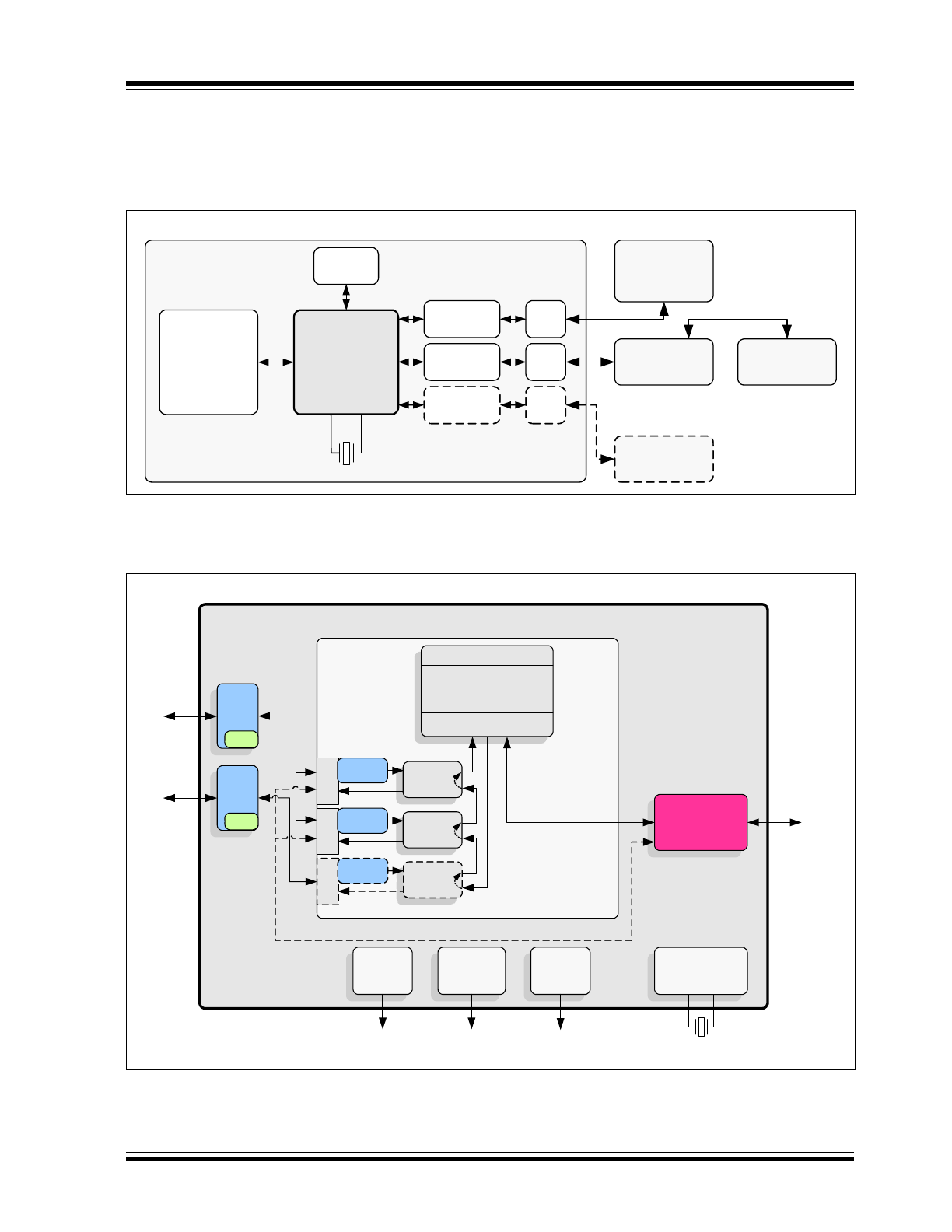
Figure 2-1
details a
typical system application, while
Figure 2-2
provides an internal block diagram of the LAN9252.
The LAN9252 can operate in Microcontroller, Expansion, or Digital I/O mode:
FIGURE 2-1:
SYSTEM BLOCK DIAGRAM
FIGURE 2-2:
INTERNAL BLOCK DIAGRAM
LAN9252
Microprocessor/
Microcontroller
Local
Bus
EEPROM
Magnetics
RJ45
25MHz
Magnetics
RJ45
EtherCAT Slave
EtherCAT
Master
EtherCAT
Slave
EtherCAT
Slave
PHY
RJ45
EtherCAT
Slave
100 PHY
w/ fiber
Registers
EtherCAT Slave Controller
SyncManager
FMMU
ESC Address Space
Registers / RAM
Loopback
Po
rt
0
Auto
Fowarder
Loopback
Po
rt 2
Auto
Fowarder
LED
Controller
To optional LEDs
System
Interrupt
Controller
IRQ
System Clocks/
Reset Controller
External
25MHz Crystal
I
2
C
EEPROM
100 PHY
w/ fiber
Registers
LAN9252
Ethernet
Ethernet
Parallel Data
Interface
To 8/16-bit
Host Bus,
MII, SPI,
Digital IOs,
GPIOs
To I
2
C
Loopback
Po
rt 1
Auto
Fowarder
MII
LAN9252
DS00001909A-page 10
2015 Microchip Technology Inc.
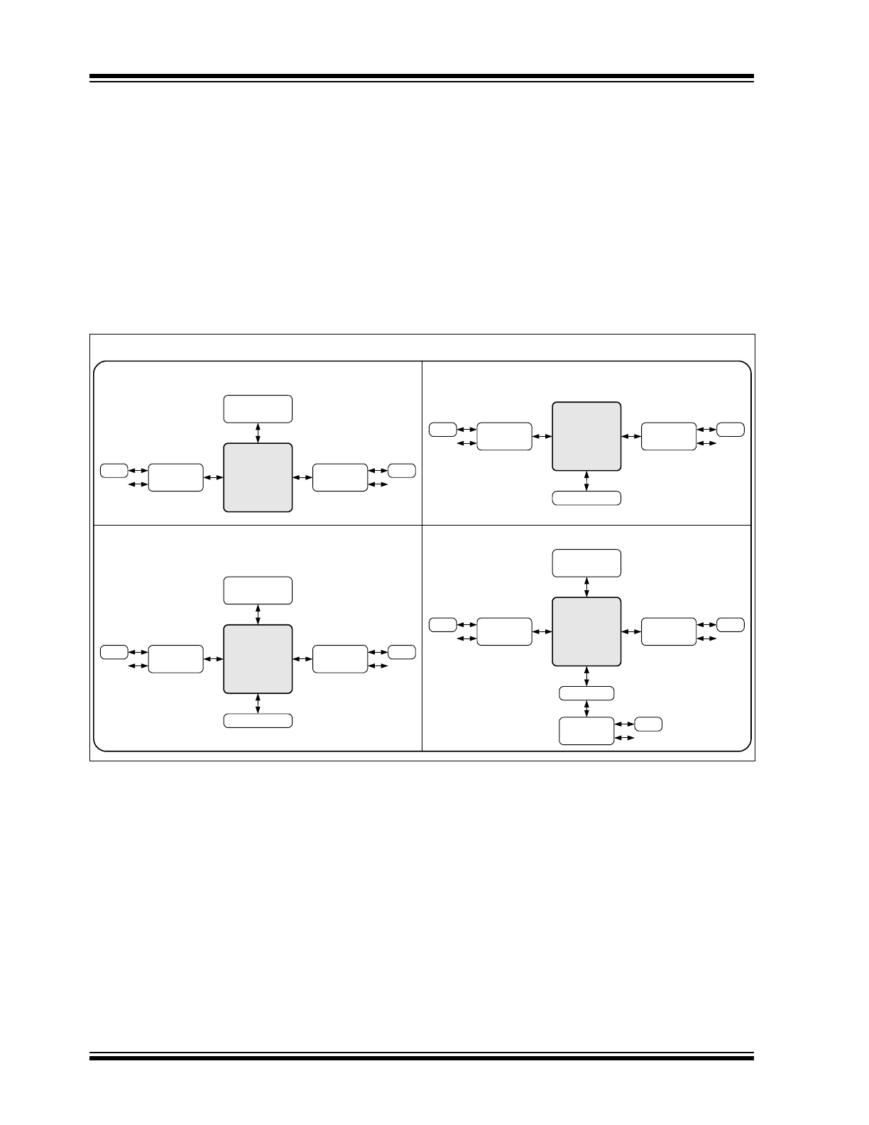
Microcontroller Mode:
The LAN9252 communicates with the microcontroller through an SRAM-like slave interface.
The simple, yet highly functional host bus interface provides a glue-less connection to most common 8 or 16-bit micro-
processors and microcontrollers as well as 32-bit microprocessors with an 8 or 16-bit external bus.
Alternatively, the device can be accessed via SPI or Quad SPI, while also providing up to 16 inputs or outputs for general
purpose usage.
Expansion Mode:
While the device is in SPI or Quad SPI mode, a third networking port can be enabled to provide an
additional MII port. This port can be connected to an external PHY, to enable star or tree network topologies, or to
another LAN9252 to create a four port solution. This port can be configured for the upstream or downstream direction.
Digital I/O Mode:
For simple digital modules without microcontrollers, the LAN9252 can operate in Digital I/O Mode
where 16 digital signals can be controlled or monitored by the EtherCAT master. Six control signals are also provided.
Figure 2-3
provides a system level overview of each mode of operation.
FIGURE 2-3:
MODES OF OPERATION
LAN9252
Microprocessor/
Microcontroller
SPI / Quad SPI
LAN9252
Microprocessor/
Microcontroller
Host Bus Interface
Magnetics or
Fiber Xcvr
RJ45
or Fiber
Magnetics or
Fiber Xcvr
RJ45
or Fiber
Magnetics or
Fiber Xcvr
RJ45
or Fiber
Magnetics or
Fiber Xcvr
RJ45
or Fiber
Microcontroller Mode
(via Host Bus Interface)
Microcontroller Mode
(via SPI)
Digital I/Os
LAN9252
PHY
MII
LAN9252
Magnetics or
Fiber Xcvr
RJ45
or Fiber
Magnetics or
Fiber Xcvr
RJ45
or Fiber
Magnetics or
Fiber Xcvr
RJ45
or Fiber
Magnetics or
Fiber Xcvr
RJ45
or Fiber
Magnetics or
Fiber Xcvr
Digital I/O Mode
Expansion Mode
GPIOs
Microprocessor/
Microcontroller
SPI / Quad SPI
RJ45
or Fiber
2015 Microchip Technology Inc.
DS00001909A-page 1
Highlights
• 2/3-port EtherCAT slave controller with 3 Fieldbus
Memory Management Units (FMMUs) and
4 SyncManagers
• Interfaces to most 8/16-bit embedded controllers
and 32-bit embedded controllers with an 8/16-bit
bus
• Integrated Ethernet PHYs with HP Auto-MDIX
• Wake on LAN (WoL) support
• Low power mode allows systems to enter sleep
mode until addressed by the Master
• Cable diagnostic support
• 1.8V to 3.3V variable voltage I/O
• Integrated 1.2V regulator for single 3.3V operation
• Low pin count and small body size package
Target Applications
• Motor Motion Control
• Process/Factory Automation
• Communication Modules, Interface Cards
• Sensors
• Hydraulic & Pneumatic Valve Systems
• Operator Interfaces
Key Benefits
• Integrated high-performance 100Mbps Ethernet
transceivers
- Compliant with IEEE 802.3/802.3u (Fast Ethernet)
- 100BASE-FX support via external fiber transceiver
- Loop-back modes
- Automatic polarity detection and correction
- HP Auto-MDIX
• EtherCAT slave controller
- Supports 3 FMMUs
- Supports 4 SyncManagers
- Distributed clock support allows synchronization with
other EtherCAT devices
- 4K bytes of DPRAM
• 8/16-Bit Host Bus Interface
- Indexed register or multiplexed bus
- Allows local host to enter sleep mode until addressed by
EtherCAT Master
- SPI / Quad SPI support
• Digital I/O Mode for optimized system cost
• 3rd port for flexible network configurations
• Comprehensive power management features
- 3 power-down levels
- Wake on link status change (energy detect)
- Magic packet wakeup, Wake on LAN (WoL), wake on
broadcast, wake on perfect DA
- Wakeup indicator event signal
• Power and I/O
- Integrated power-on reset circuit
- Latch-up performance exceeds 150mA
per EIA/JESD78, Class II
- JEDEC Class 3A ESD performance
- Single 3.3V power supply
(integrated 1.2V regulator)
• Additional Features
- Multifunction GPIOs
- Ability to use low cost 25MHz crystal for reduced BOM
• Packaging
- Pb-free RoHS compliant 64-pin QFN or 64-pin TQFP-
EP
• Available in commercial, industrial, and extended
industrial* temp. ranges
*Extended temp. (105ºC) is supported only in the 64-QFN with an
external voltage regulator (internal regulator must be disabled) and
2.5V (typ) Ethernet magnetics.
LAN9252
2/3-Port EtherCAT® Slave Controller with
Integrated Ethernet PHYs
LAN9252
DS00001909A-page 2
2015 Microchip Technology Inc.
TO OUR VALUED CUSTOMERS
It is our intention to provide our valued customers with the best documentation possible to ensure successful use of your Microchip
products. To this end, we will continue to improve our publications to better suit your needs. Our publications will be refined and
enhanced as new volumes and updates are introduced.
If you have any questions or comments regarding this publication, please contact the Marketing Communications Department via
E-mail at
docerrors@microchip.com
. We welcome your feedback.
Most Current Documentation
To obtain the most up-to-date version of this documentation, please register at our Worldwide Web site at:
http://www.microchip.com
You can determine the version of a data sheet by examining its literature number found on the bottom outside corner of any page.
The last character of the literature number is the version number, (e.g., DS30000000A is version A of document DS30000000).
Errata
An errata sheet, describing minor operational differences from the data sheet and recommended workarounds, may exist for cur-
rent devices. As device/documentation issues become known to us, we will publish an errata sheet. The errata will specify the
revision of silicon and revision of document to which it applies.
To determine if an errata sheet exists for a particular device, please check with one of the following:
• Microchip’s Worldwide Web site;
http://www.microchip.com
• Your local Microchip sales office (see last page)
When contacting a sales office, please specify which device, revision of silicon and data sheet (include -literature number) you are
using.
Customer Notification System
Register on our web site at
www.microchip.com
to receive the most current information on all of our products.
2015 Microchip Technology Inc.
DS00001909A-page 3
LAN9252
1.0 Preface ............................................................................................................................................................................................ 4
2.0 General Description ........................................................................................................................................................................ 8
3.0 Pin Descriptions and Configuration ............................................................................................................................................... 11
4.0 Power Connections ....................................................................................................................................................................... 29
5.0 Register Map ................................................................................................................................................................................. 32
6.0 Clocks, Resets, and Power Management ..................................................................................................................................... 37
7.0 Configuration Straps ..................................................................................................................................................................... 51
8.0 System Interrupts .......................................................................................................................................................................... 53
9.0 Host Bus Interface ........................................................................................................................................................................ 62
10.0 SPI/SQI Slave ........................................................................................................................................................................... 102
11.0 Ethernet PHYs .......................................................................................................................................................................... 120
12.0 EtherCAT .................................................................................................................................................................................. 196
13.0 EEPROM Interface ................................................................................................................................................................... 295
14.0 Chip Mode Configuration .......................................................................................................................................................... 296
15.0 General Purpose Timer & Free-Running Clock ........................................................................................................................ 297
16.0 Miscellaneous ........................................................................................................................................................................... 301
17.0 JTAG ......................................................................................................................................................................................... 305
18.0 Operational Characteristics ....................................................................................................................................................... 307
19.0 Package Outlines ...................................................................................................................................................................... 322
20.0 Revision History ........................................................................................................................................................................ 325
LAN9252
DS00001909A-page 4
2015 Microchip Technology Inc.
1.0
PREFACE
1.1
General Terms
TABLE 1-1:
GENERAL TERMS
Term
Description
10BASE-T
10 Mbps Ethernet, IEEE 802.3 compliant
100BASE-TX
100 Mbps Fast Ethernet, IEEE802.3u compliant
ADC
Analog-to-Digital Converter
ALR
Address Logic Resolution
AN
Auto-Negotiation
BLW
Baseline Wander
BM
Buffer Manager - Part of the switch fabric
BPDU
Bridge Protocol Data Unit - Messages which carry the Spanning Tree Protocol informa-
tion
Byte
8 bits
CSMA/CD
Carrier Sense Multiple Access/Collision Detect
CSR
Control and Status Registers
CTR
Counter
DA
Destination Address
DWORD
32 bits
EPC
EEPROM Controller
FCS
Frame Check Sequence - The extra checksum characters added to the end of an
Ethernet frame, used for error detection and correction.
FIFO
First In First Out buffer
FSM
Finite State Machine
GPIO
General Purpose I/O
Host
External system (Includes processor, application software, etc.)
IGMP
Internet Group Management Protocol
Inbound
Refers to data input to the device from the host
Level-Triggered Sticky Bit
This type of status bit is set whenever the condition that it represents is asserted. The
bit remains set until the condition is no longer true and the status bit is cleared by writ-
ing a zero.
lsb
Least Significant Bit
LSB
Least Significant Byte
LVDS
Low Voltage Differential Signaling
MDI
Medium Dependent Interface
MDIX
Media Independent Interface with Crossover
MII
Media Independent Interface
MIIM
Media Independent Interface Management
MIL
MAC Interface Layer
MLD
Multicast Listening Discovery
MLT-3
Multi-Level Transmission Encoding (3-Levels). A tri-level encoding method where a
change in the logic level represents a code bit “1” and the logic output remaining at the
same level represents a code bit “0”.
msb
Most Significant Bit
MSB
Most Significant Byte
2015 Microchip Technology Inc.
DS00001909A-page 5
LAN9252
NRZI
Non Return to Zero Inverted. This encoding method inverts the signal for a “1” and
leaves the signal unchanged for a “0”
N/A
Not Applicable
NC
No Connect
OUI
Organizationally Unique Identifier
Outbound
Refers to data output from the device to the host
PISO
Parallel In Serial Out
PLL
Phase Locked Loop
PTP
Precision Time Protocol
RESERVED
Refers to a reserved bit field or address. Unless otherwise noted, reserved bits must
always be zero for write operations. Unless otherwise noted, values are not guaran-
teed when reading reserved bits. Unless otherwise noted, do not read or write to
reserved addresses.
RTC
Real-Time Clock
SA
Source Address
SFD
Start of Frame Delimiter - The 8-bit value indicating the end of the preamble of an
Ethernet frame.
SIPO
Serial In Parallel Out
SMI
Serial Management Interface
SQE
Signal Quality Error (also known as “heartbeat”)
SSD
Start of Stream Delimiter
UDP
User Datagram Protocol - A connectionless protocol run on top of IP networks
UUID
Universally Unique IDentifier
WORD
16 bits
TABLE 1-1:
GENERAL TERMS (CONTINUED)
Term
Description
LAN9252
DS00001909A-page 6
2015 Microchip Technology Inc.
1.2
Buffer Types
TABLE 1-2:
BUFFER TYPES
Buffer Type
Description
IS
Schmitt-triggered input
VIS
Variable voltage Schmitt-triggered input
VO8
Variable voltage output with 8 mA sink and 8 mA source
VOD8
Variable voltage open-drain output with 8 mA sink
VO12
Variable voltage output with 12 mA sink and 12 mA source
VOD12
Variable voltage open-drain output with 12 mA sink
VOS12
Variable voltage open-source output with 12 mA source
VO16
Variable voltage output with 16 mA sink and 16 mA source
PU
50 µA (typical) internal pull-up. Unless otherwise noted in the pin description, internal pull-
ups are always enabled.
Internal pull-up resistors prevent unconnected inputs from floating. Do not rely on internal
resistors to drive signals external to the device. When connected to a load that must be
pulled high, an external resistor must be added.
PD
50 µA (typical) internal pull-down. Unless otherwise noted in the pin description, internal
pull-downs are always enabled.
Internal pull-down resistors prevent unconnected inputs from floating. Do not rely on internal
resistors to drive signals external to the device. When connected to a load that must be
pulled low, an external resistor must be added.
AI
Analog input
AIO
Analog bidirectional
ICLK
Crystal oscillator input pin
OCLK
Crystal oscillator output pin
ILVPECL
Low voltage PECL input pin
OLVPECL
Low voltage PECL output pin
P
Power pin
2015 Microchip Technology Inc.
DS00001909A-page 7
LAN9252
1.3
Register Nomenclature
TABLE 1-3:
REGISTER NOMENCLATURE
Register Bit Type Notation
Register Bit Description
R
Read:
A register or bit with this attribute can be read.
W
Read:
A register or bit with this attribute can be written.
RO
Read only:
Read only. Writes have no effect.
WO
Write only:
If a register or bit is write-only, reads will return unspecified data.
WC
Write One to Clear:
Writing a one clears the value. Writing a zero has no effect
WAC
Write Anything to Clear:
Writing anything clears the value.
RC
Read to Clear:
Contents is cleared after the read. Writes have no effect.
LL
Latch Low:
Clear on read of register.
LH
Latch High:
Clear on read of register.
SC
Self-Clearing:
Contents are self-cleared after the being set. Writes of zero have no
effect. Contents can be read.
SS
Self-Setting:
Contents are self-setting after being cleared. Writes of one have no
effect. Contents can be read.
RO/LH
Read Only, Latch High:
Bits with this attribute will stay high until the bit is read. After it
is read, the bit will either remain high if the high condition remains, or will go low if the
high condition has been removed. If the bit has not been read, the bit will remain high
regardless of a change to the high condition. This mode is used in some Ethernet PHY
registers.
NASR
Not Affected by Software Reset.
The state of NASR bits do not change on assertion
of a software reset.
RESERVED
Reserved Field:
Reserved fields must be written with zeros to ensure future compati-
bility. The value of reserved bits is not guaranteed on a read.
LAN9252
DS00001909A-page 8
2015 Microchip Technology Inc.
2.0
GENERAL DESCRIPTION
The LAN9252 is a 2/3-port EtherCAT slave controller with dual integrated Ethernet PHYs which each contain a full-
duplex 100BASE-TX transceiver and support 100Mbps (100BASE-TX) operation. The LAN9252 supports HP Auto-
MDIX, allowing the use of direct connect or cross-over LAN cables. 100BASE-FX is supported via an external fiber
transceiver.
The LAN9252 includes an EtherCAT slave controller with 4K bytes of Dual Port memory (DPRAM) and 3 Fieldbus Mem-
ory Management Units (FMMUs). Each FMMU performs the task of mapping logical addresses to physical addresses.
The EtherCAT slave controller also includes 4 SyncManagers to allow the exchange of data between the EtherCAT mas-
ter and the local application. Each SyncManager's direction and mode of operation is configured by the EtherCAT mas-
ter. Two modes of operation are available: buffered mode or mailbox mode. In the buffered mode, both the local
microcontroller and EtherCAT master can write to the device concurrently. The buffer within the LAN9252 will always
contain the latest data. If newer data arrives before the old data can be read out, the old data will be dropped. In mailbox
mode, access to the buffer by the local microcontroller and the EtherCAT master is performed using handshakes, guar-
anteeing that no data will be dropped.
Two user selectable host bus interface options are available:
• Indexed register access
This implementation provides three index/data register banks, each with independent Byte/WORD to DWORD
conversion. Internal registers are accessed by first writing one of the three index registers, followed by reading or
writing the corresponding data register. Three index/data register banks support up to 3 independent driver
threads without access conflicts. Each thread can write its assigned index register without the issue of another
thread overwriting it. Two 16-bit cycles or four 8-bit cycles are required within the same 32-bit index/data register -
however, these access can be interleaved. Direct (non-indexed) read and write accesses are supported to the
process data FIFOs. The direct FIFO access provides independent Byte/WORD to DWORD conversion, support-
ing interleaved accesses with the index/data registers.
• Multiplexed address/data bus
This implementation provides a multiplexed address and data bus with both single phase and dual phase address
support. The address is loaded with an address strobe followed by data access using a read or write strobe. Two
back to back 16-bit data cycles or 4 back to back 8-bit data cycles are required within the same 32-bit DWORD.
These accesses must be sequential without any interleaved accesses to other registers. Burst read and write
accesses are supported to the process data FIFOs by performing one address cycle followed by multiple read or
write data cycles.
The HBI supports 8/16-bit operation with big, little, and mixed endian operations. Two process data RAM FIFOs inter-
face the HBI to the EtherCAT slave controller and facilitate the transferring of process data information between the host
CPU and the EtherCAT slave. A configurable host interrupt pin allows the device to inform the host CPU of any internal
interrupts.
An SPI / Quad SPI slave controller provides a low pin count synchronous slave interface that facilitates communication
between the device and a host system. The SPI / Quad SPI slave allows access to the System CSRs, internal FIFOs
and memories. It supports single and multiple register read and write commands with incrementing, decrementing and
static addressing. Single, Dual and Quad bit lanes are supported with a clock rate of up to 80 MHz.
The LAN9252 supports numerous power management and wakeup features. The LAN9252 can be placed in a reduced
power mode and can be programmed to issue an external wake signal (IRQ) via several methods, including “Magic
Packet”, “Wake on LAN”, wake on broadcast, wake on perfect DA, and “Link Status Change”. This signal is ideal for
triggering system power-up using remote Ethernet wakeup events. The device can be removed from the low power state
via a host processor command or one of the wake events.
For simple digital modules without microcontrollers, the LAN9252 can also operate in Digital I/O Mode where 16 digital
signals can be controlled or monitored by the EtherCAT master.
To enable star or tree network topologies, the device can be configured as a 3-port slave, providing an additional MII
port. This port can be connected to an external PHY, forming a tap along the current daisy chain, or to another LAN9252
creating a 4-port solution. The MII port can point upstream (as Port 0) or downstream (as Port 2).
LED support consists of a standard RUN indicator and a LINK / Activity indicator per port. A 64-bit distributed clock is
included to enable high-precision synchronization and to provide accurate information about the local timing of data
acquisition.
The LAN9252 can be configured to operate via a single 3.3V supply utilizing an integrated 3.3V to 1.2V linear regulator.
The linear regulator may be optionally disabled, allowing usage of a high efficiency external regulator for lower system
power dissipation.
2015 Microchip Technology Inc.
DS00001909A-page 9
LAN9252
The LAN9252 is available in commercial, industrial, and extended industrial temperature ranges.
Figure 2-1
details a
typical system application, while
Figure 2-2
provides an internal block diagram of the LAN9252.
The LAN9252 can operate in Microcontroller, Expansion, or Digital I/O mode:
FIGURE 2-1:
SYSTEM BLOCK DIAGRAM
FIGURE 2-2:
INTERNAL BLOCK DIAGRAM
LAN9252
Microprocessor/
Microcontroller
Local
Bus
EEPROM
Magnetics
RJ45
25MHz
Magnetics
RJ45
EtherCAT Slave
EtherCAT
Master
EtherCAT
Slave
EtherCAT
Slave
PHY
RJ45
EtherCAT
Slave
100 PHY
w/ fiber
Registers
EtherCAT Slave Controller
SyncManager
FMMU
ESC Address Space
Registers / RAM
Loopback
Po
rt
0
Auto
Fowarder
Loopback
Po
rt 2
Auto
Fowarder
LED
Controller
To optional LEDs
System
Interrupt
Controller
IRQ
System Clocks/
Reset Controller
External
25MHz Crystal
I
2
C
EEPROM
100 PHY
w/ fiber
Registers
LAN9252
Ethernet
Ethernet
Parallel Data
Interface
To 8/16-bit
Host Bus,
MII, SPI,
Digital IOs,
GPIOs
To I
2
C
Loopback
Po
rt 1
Auto
Fowarder
MII
LAN9252
DS00001909A-page 10
2015 Microchip Technology Inc.
Microcontroller Mode:
The LAN9252 communicates with the microcontroller through an SRAM-like slave interface.
The simple, yet highly functional host bus interface provides a glue-less connection to most common 8 or 16-bit micro-
processors and microcontrollers as well as 32-bit microprocessors with an 8 or 16-bit external bus.
Alternatively, the device can be accessed via SPI or Quad SPI, while also providing up to 16 inputs or outputs for general
purpose usage.
Expansion Mode:
While the device is in SPI or Quad SPI mode, a third networking port can be enabled to provide an
additional MII port. This port can be connected to an external PHY, to enable star or tree network topologies, or to
another LAN9252 to create a four port solution. This port can be configured for the upstream or downstream direction.
Digital I/O Mode:
For simple digital modules without microcontrollers, the LAN9252 can operate in Digital I/O Mode
where 16 digital signals can be controlled or monitored by the EtherCAT master. Six control signals are also provided.
Figure 2-3
provides a system level overview of each mode of operation.
FIGURE 2-3:
MODES OF OPERATION
LAN9252
Microprocessor/
Microcontroller
SPI / Quad SPI
LAN9252
Microprocessor/
Microcontroller
Host Bus Interface
Magnetics or
Fiber Xcvr
RJ45
or Fiber
Magnetics or
Fiber Xcvr
RJ45
or Fiber
Magnetics or
Fiber Xcvr
RJ45
or Fiber
Magnetics or
Fiber Xcvr
RJ45
or Fiber
Microcontroller Mode
(via Host Bus Interface)
Microcontroller Mode
(via SPI)
Digital I/Os
LAN9252
PHY
MII
LAN9252
Magnetics or
Fiber Xcvr
RJ45
or Fiber
Magnetics or
Fiber Xcvr
RJ45
or Fiber
Magnetics or
Fiber Xcvr
RJ45
or Fiber
Magnetics or
Fiber Xcvr
RJ45
or Fiber
Magnetics or
Fiber Xcvr
Digital I/O Mode
Expansion Mode
GPIOs
Microprocessor/
Microcontroller
SPI / Quad SPI
RJ45
or Fiber