

2015 Microchip Technology Inc.
DS00001913A-page 1
Highlights
• 16-bit 10/100 industrial Ethernet controller & PHY
• Interfaces to most 8/16-bit embedded controllers
and 32-bit embedded controllers with an 8/16-bit
bus
• Integrated Ethernet PHY with HP Auto-MDIX
• Integrated Ethernet MAC
• Compliant with Energy Efficient Ethernet 802.3az
• Wake on LAN (WoL) support
• Integrated IEEE 1588v2 hardware time stamp unit
• Cable diagnostic support
• 1.8V to 3.3V variable voltage I/O
• Integrated 1.2V regulator for single 3.3V operation
• Low pin count and small body size package
Target Applications
• Cable, satellite, and IP set-top boxes
• Digital televisions & video recorders
• VoIP/Video phone systems
• Home gateways
• Test/Measurement equipment
• Industrial automation systems
Key Benefits
• Single-chip Ethernet controller
- Fully compliant with IEEE 802.3/802.3u standards
- Integrated Ethernet MAC and PHY
- 10BASE-T and 100BASE-TX support
- 100BASE-FX support for external fiber transceiver
- Automatic polarity detection and correction
(HP Auto-MDIX)
- Full- and Half-duplex support
- Full-duplex flow control
- Backpressure for half-duplex flow control
- Preamble generation and removal
- Automatic 32-bit CRC generation and checking
- Automatic payload padding and pad removal
- Loop-back modes
• Eliminates dropped packets
- Internal buffer memory can store over 200 packets
- Automatic PAUSE and back-pressure flow control
• Flexible address filtering modes
- One 48-bit perfect address
- 64 hash-filtered multicast addresses
- Pass all multicast
- Promiscuous mode
- Inverse filtering
- Pass all incoming with status report
- Disable reception of broadcast packets
• 8/16-Bit Host Bus Interface
- Indexed register or multiplexed bus
- 16Kbyte FIFO with flexible TX/RX allocation
- SPI / Quad SPI support
• IEEE 1588v2 hardware time stamp unit
- Global 64-bit tunable clock
- Ordinary clock: master / slave, one-step / two-step, end-
to-end / peer-to-peer delay
- Fully programmable timestamp on TX or RX,
timestamp on GPIO
- 64-bit timer comparator event generation (GPIO or IRQ)
• Comprehensive power management features
- 3 power-down levels
- Wake on link status change (energy detect)
- Magic packet wakeup, Wake on LAN (WoL), wake on
broadcast, wake on perfect DA
- Wakeup indicator event signal
- Link status change
• Power and I/O
- Integrated power-on reset circuit
- Latch-up performance exceeds 150mA
per EIA/JESD78, Class II
- JEDEC Class 3A ESD performance
- Single 3.3V power supply
(integrated 1.2V regulator)
• Additional Features
- Multifunction GPIOs
- General purpose timer
- Optional EEPROM interface
- Ability to use low cost 25MHz crystal for reduced BOM
• Packaging
- Pb-free RoHS compliant 64-pin QFN or 64-pin TQFP-
EP
• Available in commercial, industrial, and extended
industrial* temp. ranges
*Extended temp. (105ºC) is supported only in the 64-QFN with an
external voltage regulator (internal regulator must be disabled) and
2.5V (typ) Ethernet magnetics.
LAN9250
10/100 Industrial Ethernet Controller & PHY

LAN9250
DS00001913A-page 2
2015 Microchip Technology Inc.
TO OUR VALUED CUSTOMERS
It is our intention to provide our valued customers with the best documentation possible to ensure successful use of your Microchip
products. To this end, we will continue to improve our publications to better suit your needs. Our publications will be refined and
enhanced as new volumes and updates are introduced.
If you have any questions or comments regarding this publication, please contact the Marketing Communications Department via
E-mail at
docerrors@microchip.com
. We welcome your feedback.
Most Current Documentation
To obtain the most up-to-date version of this documentation, please register at our Worldwide Web site at:
http://www.microchip.com
You can determine the version of a data sheet by examining its literature number found on the bottom outside corner of any page.
The last character of the literature number is the version number, (e.g., DS30000000A is version A of document DS30000000).
Errata
An errata sheet, describing minor operational differences from the data sheet and recommended workarounds, may exist for cur-
rent devices. As device/documentation issues become known to us, we will publish an errata sheet. The errata will specify the
revision of silicon and revision of document to which it applies.
To determine if an errata sheet exists for a particular device, please check with one of the following:
• Microchip’s Worldwide Web site;
http://www.microchip.com
• Your local Microchip sales office (see last page)
When contacting a sales office, please specify which device, revision of silicon and data sheet (include -literature number) you are
using.
Customer Notification System
Register on our web site at
www.microchip.com
to receive the most current information on all of our products.

2015 Microchip Technology Inc.
DS00001913A-page 3
LAN9250
1.0 Preface ............................................................................................................................................................................................ 4
2.0 General Description ........................................................................................................................................................................ 8
3.0 Pin Descriptions and Configuration ............................................................................................................................................... 10
4.0 Power Connections ....................................................................................................................................................................... 26
5.0 Register Map ................................................................................................................................................................................. 29
6.0 Clocks, Resets, and Power Management ..................................................................................................................................... 37
7.0 Configuration Straps ..................................................................................................................................................................... 54
8.0 System Interrupts .......................................................................................................................................................................... 62
9.0 Host Bus Interface ........................................................................................................................................................................ 74
10.0 SPI/SQI Slave ........................................................................................................................................................................... 121
11.0 Host MAC .................................................................................................................................................................................. 139
12.0 Ethernet PHY ............................................................................................................................................................................ 210
13.0 I2C Master EEPROM Controller ............................................................................................................................................... 282
14.0 IEEE 1588 ................................................................................................................................................................................. 298
15.0 General Purpose Timer & Free-Running Clock ........................................................................................................................ 380
16.0 GPIO/LED Controller ................................................................................................................................................................ 384
17.0 Miscellaneous ........................................................................................................................................................................... 392
18.0 JTAG ......................................................................................................................................................................................... 397
19.0 Operational Characteristics ....................................................................................................................................................... 399
20.0 Package Outlines ...................................................................................................................................................................... 414
21.0 Revision History ........................................................................................................................................................................ 417

LAN9250
DS00001913A-page 4
2015 Microchip Technology Inc.
1.0
PREFACE
1.1
General Terms
TABLE 1-1:
GENERAL TERMS
Term
Description
10BASE-T
10 Mbps Ethernet, IEEE 802.3 compliant
100BASE-TX
100 Mbps Fast Ethernet, IEEE802.3u compliant
ADC
Analog-to-Digital Converter
ALR
Address Logic Resolution
AN
Auto-Negotiation
BLW
Baseline Wander
BM
Buffer Manager - Part of the switch fabric
BPDU
Bridge Protocol Data Unit - Messages which carry the Spanning Tree Protocol informa-
tion
Byte
8 bits
CSMA/CD
Carrier Sense Multiple Access/Collision Detect
CSR
Control and Status Registers
CTR
Counter
DA
Destination Address
DWORD
32 bits
EPC
EEPROM Controller
FCS
Frame Check Sequence - The extra checksum characters added to the end of an
Ethernet frame, used for error detection and correction.
FIFO
First In First Out buffer
FSM
Finite State Machine
GPIO
General Purpose I/O
Host
External system (Includes processor, application software, etc.)
IGMP
Internet Group Management Protocol
Inbound
Refers to data input to the device from the host
Level-Triggered Sticky Bit
This type of status bit is set whenever the condition that it represents is asserted. The
bit remains set until the condition is no longer true and the status bit is cleared by writ-
ing a zero.
lsb
Least Significant Bit
LSB
Least Significant Byte
LVDS
Low Voltage Differential Signaling
MDI
Medium Dependent Interface
MDIX
Media Independent Interface with Crossover
MII
Media Independent Interface
MIIM
Media Independent Interface Management
MIL
MAC Interface Layer
MLD
Multicast Listening Discovery
MLT-3
Multi-Level Transmission Encoding (3-Levels). A tri-level encoding method where a
change in the logic level represents a code bit “1” and the logic output remaining at the
same level represents a code bit “0”.
msb
Most Significant Bit
MSB
Most Significant Byte

2015 Microchip Technology Inc.
DS00001913A-page 5
LAN9250
NRZI
Non Return to Zero Inverted. This encoding method inverts the signal for a “1” and
leaves the signal unchanged for a “0”
N/A
Not Applicable
NC
No Connect
OUI
Organizationally Unique Identifier
Outbound
Refers to data output from the device to the host
PISO
Parallel In Serial Out
PLL
Phase Locked Loop
PTP
Precision Time Protocol
RESERVED
Refers to a reserved bit field or address. Unless otherwise noted, reserved bits must
always be zero for write operations. Unless otherwise noted, values are not guaran-
teed when reading reserved bits. Unless otherwise noted, do not read or write to
reserved addresses.
RTC
Real-Time Clock
SA
Source Address
SFD
Start of Frame Delimiter - The 8-bit value indicating the end of the preamble of an
Ethernet frame.
SIPO
Serial In Parallel Out
SMI
Serial Management Interface
SQE
Signal Quality Error (also known as “heartbeat”)
SSD
Start of Stream Delimiter
UDP
User Datagram Protocol - A connectionless protocol run on top of IP networks
UUID
Universally Unique IDentifier
WORD
16 bits
TABLE 1-1:
GENERAL TERMS (CONTINUED)
Term
Description

LAN9250
DS00001913A-page 6
2015 Microchip Technology Inc.
1.2
Buffer Types
TABLE 1-2:
BUFFER TYPES
Buffer Type
Description
IS
Schmitt-triggered input
VIS
Variable voltage Schmitt-triggered input
VO8
Variable voltage output with 8 mA sink and 8 mA source
VOD8
Variable voltage open-drain output with 8 mA sink
VO12
Variable voltage output with 12 mA sink and 12 mA source
VOD12
Variable voltage open-drain output with 12 mA sink
VOS12
Variable voltage open-source output with 12 mA source
VO16
Variable voltage output with 16 mA sink and 16 mA source
PU
50 µA (typical) internal pull-up. Unless otherwise noted in the pin description, internal pull-
ups are always enabled.
Internal pull-up resistors prevent unconnected inputs from floating. Do not rely on internal
resistors to drive signals external to the device. When connected to a load that must be
pulled high, an external resistor must be added.
PD
50 µA (typical) internal pull-down. Unless otherwise noted in the pin description, internal
pull-downs are always enabled.
Internal pull-down resistors prevent unconnected inputs from floating. Do not rely on internal
resistors to drive signals external to the device. When connected to a load that must be
pulled low, an external resistor must be added.
AI
Analog input
AIO
Analog bidirectional
ICLK
Crystal oscillator input pin
OCLK
Crystal oscillator output pin
ILVPECL
Low voltage PECL input pin
OLVPECL
Low voltage PECL output pin
P
Power pin

2015 Microchip Technology Inc.
DS00001913A-page 7
LAN9250
1.3
Register Nomenclature
TABLE 1-3:
REGISTER NOMENCLATURE
Register Bit Type Notation
Register Bit Description
R
Read:
A register or bit with this attribute can be read.
W
Read:
A register or bit with this attribute can be written.
RO
Read only:
Read only. Writes have no effect.
WO
Write only:
If a register or bit is write-only, reads will return unspecified data.
WC
Write One to Clear:
Writing a one clears the value. Writing a zero has no effect
WAC
Write Anything to Clear:
Writing anything clears the value.
RC
Read to Clear:
Contents is cleared after the read. Writes have no effect.
LL
Latch Low:
Clear on read of register.
LH
Latch High:
Clear on read of register.
SC
Self-Clearing:
Contents are self-cleared after the being set. Writes of zero have no
effect. Contents can be read.
SS
Self-Setting:
Contents are self-setting after being cleared. Writes of one have no
effect. Contents can be read.
RO/LH
Read Only, Latch High:
Bits with this attribute will stay high until the bit is read. After it
is read, the bit will either remain high if the high condition remains, or will go low if the
high condition has been removed. If the bit has not been read, the bit will remain high
regardless of a change to the high condition. This mode is used in some Ethernet PHY
registers.
NASR
Not Affected by Software Reset.
The state of NASR bits do not change on assertion
of a software reset.
RESERVED
Reserved Field:
Reserved fields must be written with zeros to ensure future compati-
bility. The value of reserved bits is not guaranteed on a read.

LAN9250
DS00001913A-page 8
2015 Microchip Technology Inc.
2.0
GENERAL DESCRIPTION
The LAN9250 is a full-featured, single-chip 10/100 Ethernet controller designed for embedded applications where per-
formance, flexibility, ease of integration and system cost control are required. The LAN9250 has been specifically
designed to provide high performance and throughput for 16-bit applications. The LAN9250 complies with the IEEE
802.3 (full/half-duplex 10BASE-T and 100BASE-TX) Ethernet protocol, IEEE 802.3az Energy Efficient Ethernet (EEE)
(100Mbps only), and the IEEE 1588v2 precision time protocol. 100BASE-FX is supported via an external fiber trans-
ceiver.
The LAN9250 includes an integrated Ethernet MAC and PHY with a high-performance SRAM-like slave interface. The
integrated checksum offload engines enable the automatic generation of the 16-bit checksum for received and trans-
mitted Ethernet frames, offloading the task from the CPU. The LAN9250 also includes large transmit and receive data
FIFOs to accommodate high latency applications. In addition, the LAN9250 memory buffer architecture allows highly
efficient use of memory resources by optimizing packet granularity.
The LAN9250 also supports features which reduce or eliminate packet loss. The internal 16-KByte SRAM can hold over
200 received packets. If the receive FIFO gets too full, the LAN9250 can automatically generate flow control packets to
the remote node, or assert back-pressure on the remote node by generating network collisions.
Two user selectable host bus interface options are available:
• Indexed register access
This implementation provides three index/data register banks, each with independent Byte/WORD to DWORD
conversion. Internal registers are accessed by first writing one of the three index registers, followed by reading or
writing the corresponding data register. Three index/data register banks support up to 3 independent driver
threads without access conflicts. Each thread can write its assigned index register without the issue of another
thread overwriting it. Two 16-bit cycles or four 8-bit cycles are required within the same 32-bit index/data register -
however, these access can be interleaved. Direct (non-indexed) read and write accesses are supported to the
packet data FIFOs. The direct FIFO access provides independent Byte/WORD to DWORD conversion, supporting
interleaved accesses with the index/data registers. Direct FIFO access also supports burst reading of the data
FIFO.
• Multiplexed address/data bus
This implementation provides a multiplexed address and data bus with both single phase and dual phase address
support. The address is loaded with an address strobe followed by data access using a read or write strobe. Two
back to back 16-bit data cycles or 4 back to back 8-bit data cycles are required within the same 32-bit DWORD.
These accesses must be sequential without any interleaved accesses to other registers. Burst read and write
accesses are supported to the packet data and status FIFOs by performing one address cycle followed by multiple
read or write data cycles.
The HBI supports 8/16-bit operation with big, little, and mixed endian operations. Four separate FIFO mechanisms (TX/
RX Data FIFO’s, TX/RX Status FIFO’s) interface the HBI to the Host MAC and facilitate the transferring of packet data
and status information between the host CPU and the device. A configurable host interrupt pin allows the device to
inform the host CPU of any internal interrupts.
An SPI / Quad SPI slave controller provides a low pin count synchronous slave interface that facilitates communication
between the device and a host system. The SPI / Quad SPI slave allows access to the System CSRs, internal FIFOs
and memories. It supports single and multiple register read and write commands with incrementing, decrementing and
static addressing. Single, Dual and Quad bit lanes are supported with a clock rate of up to 80 MHz.
The LAN9250 contains an I
2
C master EEPROM controller for connection to an optional EEPROM. This allows for the
storage and retrieval of static data. The internal EEPROM Loader can be optionally configured to automatically load
stored configuration settings from the EEPROM into the device at reset.
The LAN9250 supports numerous power management and wakeup features. The LAN9250 can be placed in a reduced
power mode and can be programmed to issue an external wake signal (PME) via several methods, including “Magic
Packet”, “Wake on LAN”, wake on broadcast, wake on perfect DA, and “Link Status Change”. This signal is ideal for
triggering system power-up using remote Ethernet wakeup events. The device can be removed from the low power state
via a host processor command or one of the wake events.
The LAN9250 can be configured to operate via a single 3.3V supply utilizing an integrated 3.3V to 1.2V linear regulator.
The linear regulator may be optionally disabled, allowing usage of a high efficiency external regulator for lower system
power dissipation.
The LAN9250 is available in commercial, industrial, and extended industrial temperature ranges.
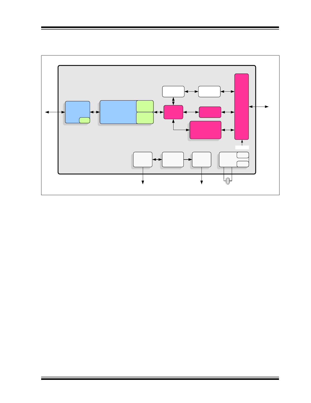
Figure 2-1
provides
an internal block diagram of the LAN9250.
2015 Microchip Technology Inc.
DS00001913A-page 9
LAN9250
FIGURE 2-1:
INTERNAL BLOCK DIAGRAM
LAN9250
GPIO/LED
Controller
To optional GPIOs/LEDs
System
Interrupt
Controller
IRQ
GP Timer
Free-Run
Clk
System
Clocks/
Reset/PME
Controller
External
25MHz Crystal
IEEE 1588v2
Clock/Events
10/100 PHY
w/fiber
w/802.3az
Registers
Ethernet
Register
Access
Mux
SPI Slave
Controller
I
2
C
EEPROM
EEPROM
Loader
PIN
Mux
Configuration
To Host bus,
SPI, I2C
TX/RX FIFOs
10/100 MAC
w/ 802.3az,
WoL & 1588v2
Registers
Host Bus
Interface

LAN9250
DS00001913A-page 10
2015 Microchip Technology Inc.
3.0
PIN DESCRIPTIONS AND CONFIGURATION
3.1
64-QFN Pin Assignments
FIGURE 3-1:
64-QFN PIN ASSIGNMENTS (TOP VIEW)
Note:
When a “#” is used at the end of the signal name, it indicates that the signal is active low. For example,
RST# indicates that the reset signal is active low.
The buffer type for each signal is indicated in the “Buffer Type” column of the pin description tables in
Sec-
tion 3.3, "Pin Descriptions"
. A description of the buffer types is provided in
Section 1.2, "Buffer Types"
.
Note: Exposed pad (VSS) on bottom of package must be connected to ground with a via field.
(Connect exposed pad to ground with a via field)
VS S
LAN9250
64-QFN
( To p V i e w)
5
6
7
8
9
10
11
12
21
22
23
24
25
26
27
28
44
43
42
41
40
39
38
37
60
59
58
57
56
55
54
53
FXLOSEN
REG_EN
FXSDA/FXLOSA/FXSDENA
RESERVED
RST#
D2/AD2/SIO2
D1/AD1/SO/SIO1
VDDIO
LED1/GPIO1/TDI/MNGT1
LED2/GPIO2/E2PSIZE
EESCL/TCK
VDDCR
D6/AD6
D3/AD3/SIO3
RBIAS
VDD12
T
X
1
VDD3
3T
XRX1
VDD3
3B
IAS
RXPA
CS
A
1
/A
LELO
D11/
A
D
11
D12/
A
D
12
VD
D
IO
D9
/A
D9
/S
C
K
TXNA
EESDA/TMS
TXPA
A2/
A
LEH
I
RXNA
VD
DC
R
IRQ
52
51
62
61
3
4
13
14
19
20
29
30
36
35
46
45
D10/
A
D
10
A3/M
NGT
2
A4/M
NGT
3
WR
/E
NB
VDDCR
VDD33
OSCVSS
OSCVDD12
VDD1
2T
X2
RESERVED
RESERVED
RESERVED
TESTMODE
D8/AD8
D7/AD7
VDDIO
1
2
OSCO
OSCI
16
15
D13/AD13
D14/AD14
17
18
D0
/A
D0
/S
I/
SI
O
0
PM
E
32
VD
D
IO
RD
/R
D_WR
31
34
33
A0/D15/AD15
FIFOSEL
48
VDDIO
47
LED0/GPIO0/TDO/MNGT0
50
49
D5/AD5/SCS#
D4/AD4
64
RESERVED
VDD3
3T
XRX2
63