

2006-2017 Microchip Technology Inc.
DS
00002417A
-page 1
Highlights
• Efficient architecture with low CPU overhead
• Easily interfaces to most 16-bit embedded CPU’s
• 1.8V to 3.3V variable voltage I/O accommodates
wide range of I/O signalling without voltage level
shifters
• Integrated PHY with HP Auto-MDIX support
• Integrated checksum offload engine helps reduce
CPU load
• Low pin count and small body size package for
small form factor system designs
Target Applications
• Cable, satellite, and IP set-top boxes
• Digital video recorders
• Video-over IP solutions, IP PBX & video phones
• Wireless routers & access points
• Audio distribution systems
• Printers, kiosks, security systems
• General embedded applications
Key Benefits
• Non-PCI Ethernet controller for standard perfor-
mance applications
- 16-bit interface
- Burst-mode read support
• Minimizes dropped packets
- Internal buffer memory can store over 200
packets
- Automatic PAUSE and back-pressure flow
control
• Minimizes CPU overhead
- Supports Slave-DMA
- Interrupt Pin with Programmable Hold-off
timer
• Reduces system cost and increases design flexi-
bility
• SRAM-like interface easily interfaces to most
embedded CPU’s or SoC’s
• Reduced Power Modes
- Numerous power management modes
- Wake on LAN
- Magic packet wakeup
- Wakeup indicator event signal
- Link Status Change
• Single chip Ethernet controller
- Fully compliant with IEEE 802.3/802.3u stan-
dards
- Integrated Ethernet MAC and PHY
- 10BASE-T and 100BASE-TX support
- Full- and Half-duplex support
- Full-duplex flow control
- Backpressure for half-duplex flow control
- Preamble generation and removal
- Automatic 32-bit CRC generation and
checking
- Automatic payload padding and pad removal
- Loop-back modes
• Flexible address filtering modes
- One 48-bit perfect address
- 64 hash-filtered multicast addresses
- Pass all multicast
- Promiscuous mode
- Inverse filtering
- Pass all incoming with status report
- Disable reception of broadcast packets
• Integrated 10/100 Ethernet PHY
- Supports HP Auto-MDIX
- Auto-negotiation
- Supports energy-detect power down
• Host bus interface
- Simple, SRAM-like interface
- 16-bit data bus
- 16Kbyte FIFO with flexible TX/RX allocation
- One configurable host interrupt
• Miscellaneous features
- Small form factor, 56-pin QFN RoHS Compli-
ant package
- Integrated 1.8V regulator
- Integrated checksum offload engine
- Mixed endian support
- General Purpose Timer
- Optional EEPROM interface
- Support for 3 status LEDs multiplexed with
Programmable GPIO signals
• Single 3.3V Power Supply with Variable Voltage
I/O
• 0
C to +70C Commercial Temperature Support
LAN9220
16-bit Non-PCI Small Form Factor 10/100 Ethernet Controller
with Variable Voltage I/O & HP Auto-MDIX Support

LAN9220
DS
00002417A
-page 2
2006-2017 Microchip Technology Inc.
TO OUR VALUED CUSTOMERS
It is our intention to provide our valued customers with the best documentation possible to ensure successful use of your Microchip
products. To this end, we will continue to improve our publications to better suit your needs. Our publications will be refined and
enhanced as new volumes and updates are introduced.
If you have any questions or comments regarding this publication, please contact the Marketing Communications Department via
E-mail at
docerrors@microchip.com
. We welcome your feedback.
Most Current Data Sheet
To obtain the most up-to-date version of this data sheet, please register at our Worldwide Web site at:
http://www.microchip.com
You can determine the version of a data sheet by examining its literature number found on the bottom outside corner of any page.
The last character of the literature number is the version number, (e.g., DS30000000A is version A of document DS30000000).
Errata
An errata sheet, describing minor operational differences from the data sheet and recommended workarounds, may exist for cur-
rent devices. As device/documentation issues become known to us, we will publish an errata sheet. The errata will specify the
revision of silicon and revision of document to which it applies.
To determine if an errata sheet exists for a particular device, please check with one of the following:
• Microchip’s Worldwide Web site;
http://www.microchip.com
• Your local Microchip sales office (see last page)
When contacting a sales office, please specify which device, revision of silicon and data sheet (include -literature number) you are
using.
Customer Notification System
Register on our web site at
www.microchip.com
to receive the most current information on all of our products.

2006-2017 Microchip Technology Inc.
DS
00002417A
-page 3
LAN9220
Table of Contents
1.0 General Description ........................................................................................................................................................................ 4
2.0 Pin Description and Configuration .................................................................................................................................................. 8
3.0 Functional Description .................................................................................................................................................................. 15
4.0 Internal Ethernet PHY ................................................................................................................................................................... 57
5.0 Register Description ...................................................................................................................................................................... 66
6.0 Timing Diagrams ......................................................................................................................................................................... 114
7.0 Operational Characteristics ......................................................................................................................................................... 126
8.0 Package Information ................................................................................................................................................................... 135
Appendix A: Data Sheet Revision History ......................................................................................................................................... 137

LAN9220
DS
00002417A
-page 4
2006-2017 Microchip Technology Inc.
1.0
GENERAL DESCRIPTION
The LAN9220 is a full-featured, single-chip 10/100 Ethernet controller designed for embedded applications where per-
formance, flexibility, ease of integration and system cost control are required. The LAN9220 is fully IEEE 802.3
10BASE-T and 802.3u 100BASE-TX compliant, and supports HP Auto-MDIX. The variable voltage I/O signals of the
LAN9220 accommodate lower voltage I/O signalling without the need for voltage level shifters.
The LAN9220 includes an integrated Ethernet MAC and PHY with a high-performance SRAM-like slave interface. The
simple, yet highly functional host bus interface provides a glue-less connection to most common 16-bit microprocessors
and microcontrollers as well as 32-bit microprocessors with a 16-bit external bus. The integrated checksum offload
engines enable the automatic generation of the 16-bit checksum for received and transmitted Ethernet frames, offload-
ing the task from the CPU. The LAN9220 also includes large transmit and receive data FIFOs to accommodate high
latency applications. In addition, the LAN9220 memory buffer architecture allows highly efficient use of memory
resources by optimizing packet granularity.
Applications
The LAN9220 is well suited for many embedded applications, including:
• Printers, kiosks, POS terminals and security systems
• Audio distribution systems
• General embedded systems
• Basic cable, satellite and IP set-top boxes
• Voice-over-IP solutions
The LAN9220 also supports features which reduce or eliminate packet loss. Its internal 16-KByte SRAM can hold over
200 received packets. If the receive FIFO gets too full, the LAN9220 can automatically generate flow control packets to
the remote node, or assert back-pressure on the remote node by generating network collisions.
The LAN9220 supports numerous power management and wakeup features. The LAN9220 can be placed in a reduced
power mode and can be programmed to issue an external wake signal via several methods, including “Magic Packet”,
“Wake on LAN” and “Link Status Change”. This signal is ideal for triggering system power-up using remote Ethernet
wakeup events. The device can be removed from the low power state via a host processor command.
2006-2017 Microchip Technology Inc.
DS
00002417A
-page 5
LAN9220
1.1
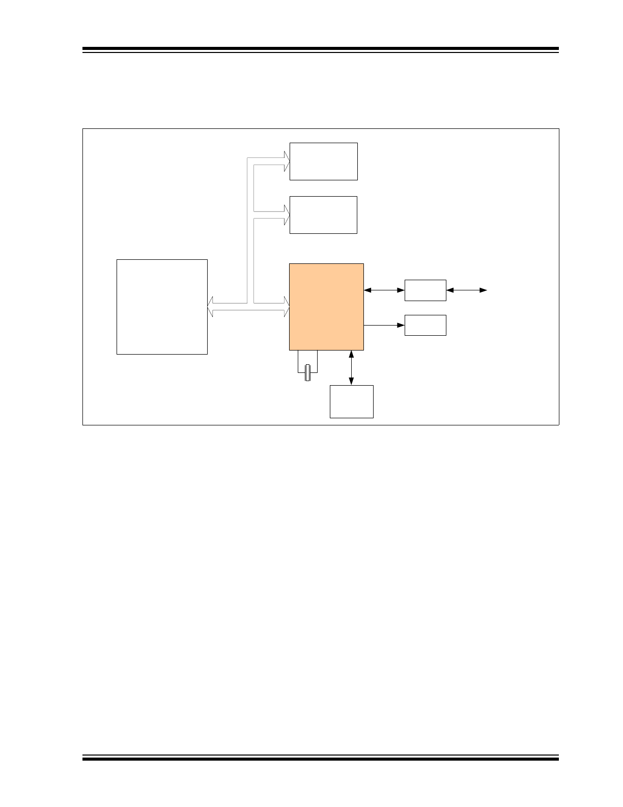
Block Diagram
The Microchip LAN9220 integrated 10/100 MAC/PHY controller is a peripheral chip that performs the function of trans-
lating parallel data from a host controller into Ethernet packets. The LAN9220 Ethernet MAC/PHY controller is designed
and optimized to function in an embedded environment. All communication is performed with programmed I/O transac-
tions using the simple SRAM-like host interface bus.
The diagram shown above, describes a typical system configuration of the LAN9220 in a typical embedded environ-
ment.
The LAN9220 is a general purpose, platform independent, Ethernet controller. The LAN9220 consists of four major func-
tional blocks. The four blocks are:
• 10/100 Ethernet PHY
• 10/100 Ethernet MAC
• RX/TX FIFOs
• Host Bus Interface (HBI)
FIGURE 1-1:
SYSTEM BLOCK DIAGRAM
Microprocessor/
Microcontroller
LAN9220
Magnetics
Ethernet
System
Peripherals
System Memory
EEPROM
(Optional)
LEDS/
GPIO
25MHz
XTAL
System Bus
LAN9220
DS
00002417A
-page 6
2006-2017 Microchip Technology Inc.
1.2
Internal Block Overview
This section provides an overview of each of these functional blocks as shown in Figure 1-2, "Internal Block Diagram".
FIGURE 1-2:
INTERNAL BLOCK DIAGRAM
1.3
10/100 Ethernet PHY
The LAN9220 integrates an IEEE 802.3 physical layer for twisted pair Ethernet applications. The PHY can be configured
for either 100 Mbps (100BASE-TX) or 10 Mbps (10BASE-T) Ethernet operation in either full or half duplex configura-
tions. The PHY block supports HP Auto-MDIX and auto-negotiation.
Minimal external components are required for the utilization of the Integrated PHY.
1.4
10/100 Ethernet MAC
The transmit and receive data paths are separate within the MAC allowing the highest performance especially in full
duplex mode. The data paths connect to the PIO interface Function via separate busses to increase performance. Pay-
load data as well as transmit and receive status is passed on these busses.
A third internal bus is used to access the MAC’s Control and Status Registers (CSR’s). This bus is accessible from the
host through the PIO interface function.
On the backend, the MAC interfaces with the internal 10/100 PHY through a MII (Media Independent Interface) port
internal to the LAN9220. The MAC CSR's also provide a mechanism for accessing the PHY’s internal registers through
the internal SMI (Serial Management Interface) bus.
The MAC Interface Layer (MIL), within the MAC, contains a 2K Byte transmit and a 128 Byte receive FIFO which is sep-
arate from the TX and RX FIFOs. The FIFOs within the MAC are not directly accessible from the host interface. The
differentiation between the TX/RX FIFO memory buffers and the MAC buffers is that when the transmit or receive pack-
ets are in the MAC buffers, the host no longer can control or access the TX or RX data. The MAC buffers (both TX and
RX) are in effect the working buffers of the Ethernet MAC logic. In the case of reception, the data must be moved first
to the RX FIFOs for the host to access the data. For TX operations, the MIL operates in store-and-forward mode and
will queue an entire frame before beginning transmission.
10/100
Ethernet
PHY
10/100
Ethernet
MAC
2kB to 14kB
Configurable TX FIFO
2kB to 14kB
Configurable RX FIFO
Interrupt
Controller
GP Timer
PIO
Controller
3.3V to 1.8V
Core Regulator
PLL
25MHz
+3.3V
EEPROM
Controller
EEPROM
(Optional )
RX Status FIFO
TX Status FIFO
MIL - TX Elastic
Buffer - 2K bytes
MIL - RX Elastic
Buffer - 128 bytes
Power
Management
IRQ
FIFO _SEL
PME
Wakup Indicator
Host Bus Interface
(HBI)
16-bit SRAM I/F
RX Checksum
Offload Engine
TX Checksum
Offload Engine
LAN

2006-2017 Microchip Technology Inc.
DS
00002417A
-page 7
LAN9220
1.5
Receive and Transmit FIFOs
The Receive and Transmit FIFOs allow increased packet buffer storage to the MAC. The FIFOs are a conduit between
the host interface and the MAC through which all transmitted and received data and status information is passed. Deep
FIFOs allow a high degree of latency tolerance relative to the various transport and OS software stacks thus reducing
or minimizing overrun conditions. Like the MAC, the FIFOs have separate receive and transmit data paths. In addition,
the RX and TX FIFOs are configurable in size, allowing increased flexibility.
1.6
Interrupt Controller
The LAN9220 supports a single programmable interrupt. The programmable nature of this interrupt allows the user the
ability to optimize performance dependent upon the application requirement. Both the polarity and buffer type of the
interrupt pin are configurable for the external interrupt processing. The interrupt line can be configured as an open-drain
output to facilitate the sharing of interrupts with other devices. In addition, a programmable interrupt de-assertion interval
is provided.
1.7
GPIO Interface
A 3-bit GPIO and 2-bit GPO (Multiplexed on the EEPROM and LED Pins) interface is included in the LAN9220. It is
accessible through the host bus interface via the CSRs. The GPIO signals can function as inputs, push-pull outputs and
open drain outputs. The GPIO’s (GPO’s are not configurable) can also be configured to trigger interrupts with program-
mable polarity.
1.8
Serial EEPROM Interface
A serial EEPROM interface is included in the LAN9220. The serial EEPROM is optional and can be programmed with
the LAN9220 MAC address. The LAN9220 can optionally load the MAC address automatically after hardware reset, or
soft reset.
1.9
Power Management Controls
The LAN9220 supports comprehensive array of power management modes to allow use in power sensitive applications.
Wake on LAN, Link Status Change and Magic Packet detection are supported by the LAN9220. An external PME (Power
Management Event) interrupt is provided to indicate detection of a wakeup event.
1.10
General Purpose Timer
The general-purpose timer has no dedicated function within the LAN9220 and may be programmed to issue a timed
interrupt.
1.11
Host Bus Interface (SRAM Interface)
The host bus interface provides a FIFO interface for the transmit and receive data paths, as well as an interface for the
LAN9220 Control and Status Registers (CSR’s).
The host bus interface is the primary bus for connection to the embedded host system. This interface models an asyn-
chronous SRAM. TX FIFO, RX FIFO, and CSR’s are accessed through this interface. Programmed I/O transactions are
supported.
The LAN9220 host bus interface supports 16-bit bus transfers. Internally, all data paths are 32-bits wide. The LAN9220
can be interfaced to either Big-Endian or Little-Endian processors and includes mixed endian support for FIFO
accesses.
LAN9220
DS
00002417A
-page 8
2006-2017 Microchip Technology Inc.
2.0
PIN DESCRIPTION AND CONFIGURATION
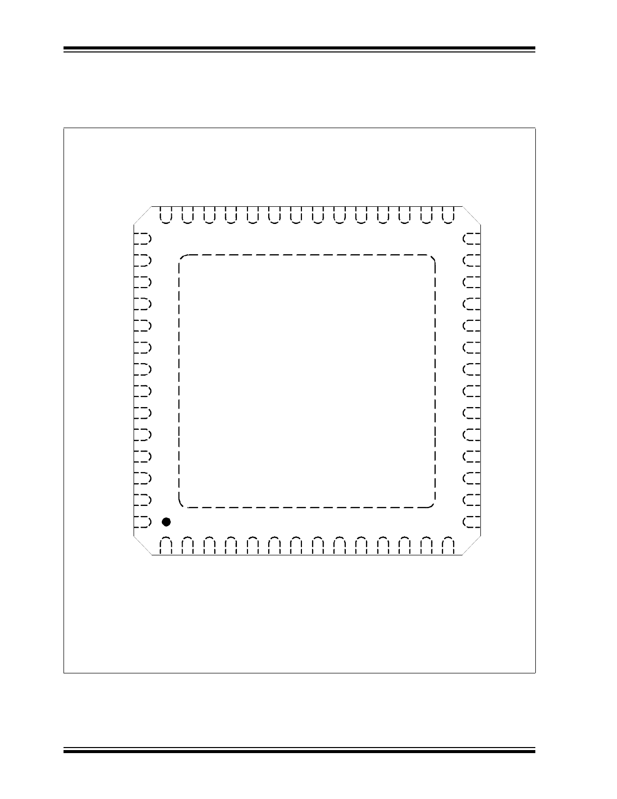
FIGURE 2-1:
56-QFN PIN CONFIGURATION (TOP VIEW)
VSS
NOTE: Exposed pad (VSS) on bottom of package must be connected to ground
**DENOTES A MULTIFUNCTION PIN
NOTE: When HP Auto-MDIX is activated, the TPO+/- pins can function as TPI +/- and vice-versa
LAN9220
56-QFN
(TOP VIEW)
IRQ
nR
ESET
D7
TEST
1
2
3
4
5
6
7
8
9
10
11
12
13
14
15
16
17
18
19
20
21
22
23
24
25
26
27
28
42
41
40
39
38
37
36
35
34
33
32
31
30
29
56
55
54
53
52
51
50
49
48
47
46
45
44
43
FI
FO
_S
EL
A1
A2
A3
A4
A5
A6
A7
GP
IO
2/
nL
ED
3*
*
GP
IO
1/
nL
ED
2*
*
GP
IO
0/
nL
ED
1*
*
VD
D1
8C
O
R
E
VD
D
33
R
EG
PM
E
EEC
LK
/G
PO
4*
*
EEC
S
EED
IO
/G
PO
3*
*
VDD1
8C
O
RE
D0
D1
D2
D3
D4
D5
VDDV
AR
IO
D6
TPO-
TPO+
VDD33A
TPI-
TPI+
VDD33A
EXRES
VDD33A
AMDIX_EN
VDD18A
XTAL2
XTAL1/CLKIN**
VDDVARIO
D8
D9
D10
VDDVARIO
D11
D12
D13
D14
D15
VDDVARIO
nCS
nWR
nRD

2006-2017 Microchip Technology Inc.
DS
00002417A
-page 9
LAN9220
2.1
Pin List
TABLE 2-1:
HOST BUS INTERFACE SIGNALS
Name
Symbol
Buffer
Type
#
Pins
Description
Host Data
D[15:0]
VIS/VO8
16
Bi-directional data port.
Host Address
A[7:1]
VIS
7
7-bit Address Port. Used to select Internal CSR’s and
TX and RX FIFOs.
Read Strobe
nRD
VIS
1
Active low strobe to indicate a read cycle.
Write Strobe
nWR
VIS
1
Active low strobe to indicate a write cycle. This signal,
qualified with nCS, is also used to wakeup the
LAN9220 when it is in a reduced power state.
Chip Select
nCS
VIS
1
Active low signal used to qualify read and write
operations. This signal qualified with nWR is also used
to wakeup the LAN9220 when it is in a reduced power
state.
Interrupt
Request
IRQ
VO8/
VOD8
1
Programmable Interrupt request. Programmable
polarity, source and buffer types.
FIFO Select
FIFO_SEL
VIS
1
When driven high all accesses to the LAN9220 are to
the RX or TX Data FIFOs. In this mode, the A[7:3]
upper address inputs are ignored.
TABLE 2-2:
LAN INTERFACE SIGNALS
Name
Symbol
Buffer
Type
# Pins
Description
TPO+
TPO+
AO
1
Transmit Positive Output (normal)
Receive Positive Input (reversed)
TPO-
TPO-
AO
1
Transmit Negative Output (normal)
Receive Negative Input (reversed)
TPI+
TPI+
AI
1
Receive Positive Input (normal)
Transmit Positive Input (reversed)
TPI-
TPI-
AI
1
Receive Negative Input (normal)
Transmit Negative Output (reversed)
PHY External Bias
Resistor
EXRES
AI
1
Must be connected to ground through a 12.4K
ohm 1% resistor.
Note:
The pin names for the twisted pair pins shown above apply to a normal connection. If HP Auto-MDIX is
enabled and a reverse connection is detected, or a reverse connection is manually selected, the input pins
become outputs, and vice-versa, as indicated in the descriptions.

LAN9220
DS
00002417A
-page 10
2006-2017 Microchip Technology Inc.
TABLE 2-3:
SERIAL EEPROM INTERFACE SIGNALS
Name
Symbol
Buffer
Type
# Pins
Description
EEPROM Data,
GPO3, TX_EN,
TX_CLK
EEDIO/GPO3/
TX_EN/TX_CLK
VIS/VO8
1
EEPROM Data: This bi-directional pin can be
connected to a serial EEPROM DIO. This is
optional.
General Purpose Output 3: This pin can also
function as a general purpose output, or it can
be configured to monitor the TX_EN or
TX_CLK signals on the internal MII port. When
configured as a GPO signal, or as a
TX_EN/TX_CLK monitor, the EECS pin is
deasserted so as to never unintentionally
access the serial EEPROM. This signal cannot
function as a general-purpose input.
EEPROM Chip
Select
EECS
VO8
1
Serial EEPROM chip select.
EEPROM Clock,
GPO4 RX_DV,
RX_CLK
EECLK/GPO4/
RX_DV/RX_CLK
VO8
(PU)
1
EEPROM Clock: Serial EEPROM Clock pin.
General Purpose Output 4: This pin can also
function as a general-purpose output, or it can
be configured to monitor the RX_DV or
RX_CLK signals on the internal MII port. When
configured as a GPO signal, or as an
RX_DV/RX_CLK monitor, the EECS pin is
deasserted so as to never unintentionally
access the serial EEPROM. This signal cannot
function as a general-purpose input.
Note:
When the EEPROM interface is not
used, the EECLK pin must be left
unconnected.
Note:
When operating at reduced
VDDVARIO voltage levels (less
than 3.0V), this pin must be pulled-
up with an external resistor. Refer to
Section 2.2, "External Pull-Up/Pull-
Down Resistors"
for more informa-
tion.
Note:
This pin must not be pulled low by
an external resistor or driven low
externally under any conditions.