

2011-2016 Microchip Technology Inc.
DS00002276A-page 1
Highlights
• Single Chip Ethernet Controller
• Dual Speed - 10/100 Mbps
• Fully Supports Full Duplex Switched Ethernet
• Supports Burst Data Transfer
• 8 Kbytes Internal Memory for Receive and Trans-
mit FIFO Buffers
• Enhanced Power Management Features
• Optional Configuration via Serial EEPROM Inter-
face
• Supports 8, 16 and 32 Bit CPU Accesses
• Internal 32 Bit Wide Data Path (Into Packet Buffer
Memory)
• Built-in Transparent Arbitration for Slave Sequen-
tial Access Architecture
• Flat MMU Architecture with Symmetric Transmit
and Receive Structures and Queues
• 3.3V Operation with 5V Tolerant IO Buffers (See
Pin List Description for Additional Details)
• Single 25 MHz Reference Clock for Both PHY and
MAC
• External 25Mhz-output pin for an external PHY
supporting PHYs physical media.
• Low Power CMOS Design
• Supports Multiple Embedded Processor Host
Interfaces
- ARM
- SH
- Power PC
- Coldfire
- 680X0, 683XX
- MIPS R3000
• 3.3V MII (Media Independent Interface) MAC-
PHY Interface Running at Nibble Rate
• MII Management Serial Interface
• 128-Pin QFP RoHS compliant package
• 128-Pin TQFP 1.0 mm height RoHS compliant
package
• Commercial Temperature Range from 0
C to
70
C (LAN91C111)
• Industrial Temperature Range from -40
C to 85C
(LAN91C111i)
Network Interface
• Fully Integrated IEEE 802.3/802.3u-100Base-TX/
10Base-T Physical Layer
• Auto-Negotiation: 10/100, Full / Half Duplex
• On Chip Wave Shaping - No External Filters
Required
• Adaptive Equalizer
• Baseline Wander Correction
• LED Outputs (User selectable – Up to 2 LED func-
tions at one time)
- Link
- Activity
- Full Duplex
- 10/100
- Transmit
- Receive
LAN91C111
10/100 Non-PCI Ethernet Single Chip MAC + PHY

LAN91C111
DS00002276A-page 2
2011-2016 Microchip Technology Inc.
TO OUR VALUED CUSTOMERS
It is our intention to provide our valued customers with the best documentation possible to ensure successful use of your Microchip
products. To this end, we will continue to improve our publications to better suit your needs. Our publications will be refined and
enhanced as new volumes and updates are introduced.
If you have any questions or comments regarding this publication, please contact the Marketing Communications Department via
E-mail at
docerrors@microchip.com
. We welcome your feedback.
Most Current Data Sheet
To obtain the most up-to-date version of this data sheet, please register at our Worldwide Web site at:
http://www.microchip.com
You can determine the version of a data sheet by examining its literature number found on the bottom outside corner of any page.
The last character of the literature number is the version number, (e.g., DS30000000A is version A of document DS30000000).
Errata
An errata sheet, describing minor operational differences from the data sheet and recommended workarounds, may exist for cur-
rent devices. As device/documentation issues become known to us, we will publish an errata sheet. The errata will specify the
revision of silicon and revision of document to which it applies.
To determine if an errata sheet exists for a particular device, please check with one of the following:
• Microchip’s Worldwide Web site;
http://www.microchip.com
• Your local Microchip sales office (see last page)
When contacting a sales office, please specify which device, revision of silicon and data sheet (include -literature number) you are
using.
Customer Notification System
Register on our web site at
www.microchip.com
to receive the most current information on all of our products.

2011-2016 Microchip Technology Inc.
DS00002276A-page 3
LAN91C111
Table of Contents
1.0 General Description ........................................................................................................................................................................ 4
2.0 Pin Configurations ........................................................................................................................................................................... 5
3.0 Block Diagrams ............................................................................................................................................................................... 7
4.0 Signal Descriptions ....................................................................................................................................................................... 10
5.0 Description of Pin Functions ......................................................................................................................................................... 11
6.0 Signal Description Parameters ..................................................................................................................................................... 15
7.0 Functional Description .................................................................................................................................................................. 16
8.0 MAC Data Structures and Registers ............................................................................................................................................. 38
9.0 PHY MII Registers ....................................................................................................................................................................... 65
10.0 Software Driver and Hardware Sequence Flow .......................................................................................................................... 77
11.0 Board Setup Information ............................................................................................................................................................. 88
12.0 Application Considerations ......................................................................................................................................................... 90
13.0 Operational Description .............................................................................................................................................................. 97
14.0 Timing Diagrams ....................................................................................................................................................................... 102
15.0 Package Outlines ...................................................................................................................................................................... 118
Appendix A: Data Sheet Revision History ......................................................................................................................................... 120
The Microchip Web Site .................................................................................................................................................................... 121
Customer Change Notification Service ............................................................................................................................................. 121
Customer Support ............................................................................................................................................................................. 121
Product Identification System ........................................................................................................................................................... 122

LAN91C111
DS00002276A-page 4
2011-2016 Microchip Technology Inc.
1.0
GENERAL DESCRIPTION
The Microchip LAN91C111 is designed to facilitate the implementation of a third generation of Fast Ethernet connectivity
solutions for embedded applications. For this third generation of products, flexibility and integration dominate the design
requirements. The LAN91C111 is a mixed signal Analog/Digital device that implements the MAC and PHY portion of the
CSMA/CD protocol at 10 and 100 Mbps. The design will also minimize data throughput constraints utilizing a 32-bit, 16-
bit or 8-bit bus Host interface in embedded applications.
The total internal memory FIFO buffer size is 8 Kbytes, which is the total chip storage for transmit and receive opera-
tions.
The Microchip LAN91C111 is software compatible with the LAN9000 family of products.
Memory management is handled using a patented optimized MMU (Memory Management Unit) architecture and a 32-
bit wide internal data path. This I/O mapped architecture can sustain back-to-back frame transmission and reception for
superior data throughput and optimal performance. It also dynamically allocates buffer memory in an efficient buffer uti-
lization scheme, reducing software tasks and relieving the host CPU from performing these housekeeping functions.
The Microchip LAN91C111 provides a flexible slave interface for easy connectivity with industry-standard buses. The
Bus Interface Unit (BIU) can handle synchronous as well as asynchronous transfers, with different signals being used
for each one. Asynchronous bus support for ISA is supported even though ISA cannot sustain 100 Mbps traffic. Fast
Ethernet data rates are attainable for ISA-based nodes on the basis of the aggregate traffic benefits.
Two different interfaces are supported on the network side. The first Interface is a standard Magnetics transmit/receive
pair interfacing to 10/100Base-T utilizing the internal physical layer block. The second interface follows the MII (Media
Independent Interface) specification standard, consisting of 4 bit wide data transfers at the nibble rate. This interface is
applicable to 10 Mbps standard Ethernet or 100 Mbps Ethernet networks. Three of the LAN91C111’s pins are used to
interface to the two-line MII serial management protocol.
The Microchip LAN91C111 integrates IEEE 802.3 Physical Layer for twisted pair Ethernet applications. The PHY can
be configured for either 100 Mbps (100Base-TX) or 10 Mbps (10Base-T) Ethernet operation. The Analog PHY block
consists of a 4B5B/Manchester encoder/decoder, scrambler/de-scrambler, transmitter with wave shaping and output
driver, twisted pair receiver with on chip equalizer and baseline wander correction, clock and data recovery, Auto-Nego-
tiation, controller interface (MII), and serial port (MI). Internal output wave shaping circuitry and on-chip filters eliminate
the need for external filters normally required in 100Base-TX and 10Base-T applications.
The LAN91C111 can automatically configure itself for 100 or 10 Mbps and Full or Half Duplex operation with the on-chip
Auto-Negotiation algorithm. The LAN91C111 is ideal for media interfaces for embedded application desiring Ethernet
connectivity as well as 100Base-TX/10Base-T adapter cards, motherboards, repeaters, switching hubs. The
LAN91C111 operates from a single 3.3V supply. The inputs and outputs of the host Interface are 5V tolerant and will
directly interface to other 5V devices.
2011-2016 Microchip Technology Inc.
DS00002276A-page 5
LAN91C111
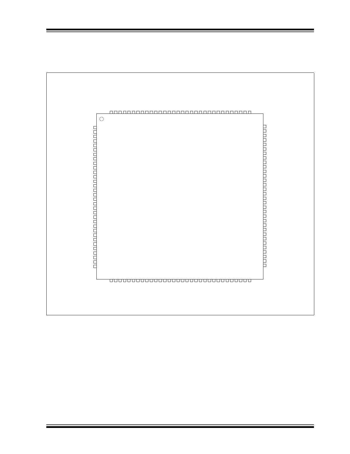
2.0
PIN CONFIGURATIONS
FIGURE 2-1:
PIN CONFIGURATION - LAN91C111-FEAST 128-PIN TQFP
33
34
35
36
37
38
39
40
41
42
43
44
45
46
47
48
49
50
51
52
53
54
55
56
57
58
59
60
61
62
63
64
128
127
126
125
124
123
122
121
120
119
118
117
116
115
114
113
112
111
110
109
108
107
106
105
104
103
102
101
100
99
98
97
96
95
94
93
92
91
90
89
88
87
86
85
84
83
82
81
80
79
78
77
76
75
74
73
72
71
70
69
68
67
66
65
1
2
3
4
5
6
7
8
9
10
11
12
13
14
15
16
17
18
19
20
21
22
23
24
25
26
27
28
29
30
31
32
nBE2
nBE1
nBE0
GND
A15
A14
A13
A12
A11
A10
A9
A8
A7
A6
A5
A4
A3
A2
A1
VDD
D8
D9
D10
D11
GND
D12
D13
D14
D15
GND
D16
D17
VDD
nCSOUT
IOS0
IOS1
IOS2
ENEEP
EEDO
EEDI
EESK
EECS
AVDD
RBIAS
AGND
TPO+
TPO-
AVDD
TPI+
TPI-
AGND
nLNK
LBK
nLEDA
nLEDB
GND
MDI
MDO
MCLK
nCNTRL
INTR0
RESET
nRD
nWR
XTAL2
XTAL1
RX_
E
R
RX_
D
V
RXD0
RXD1
RXD2
RXD3
VDD
CRS1
0
0
RX2
5
GN
D
TXD0
TXD1
TXD2
TXD3
C
O
L100
TXEN100
VDD
TX25
GN
D
D0
D1
D2
D3
GN
D
D4
D5
D6
D7
VDD
nBE3
VDD
nDATACS
nCYCLE
W/nR
nADS
ARDY
GN
D
nVLBUS
AEN
LCLK
nSRDY
VDD
nLDEV
nRDYRTN
X25OU
T
D3
1
D3
0
D2
9
D2
8
GN
D
D2
7
D2
6
D2
5
D2
4
GN
D
D2
3
D2
2
D2
1
D2
0
VDD
D1
9
D1
8
LAN91C111-
FEAST
TM
128 PIN TQFP
LAN91C111
DS00002276A-page 6
2011-2016 Microchip Technology Inc.
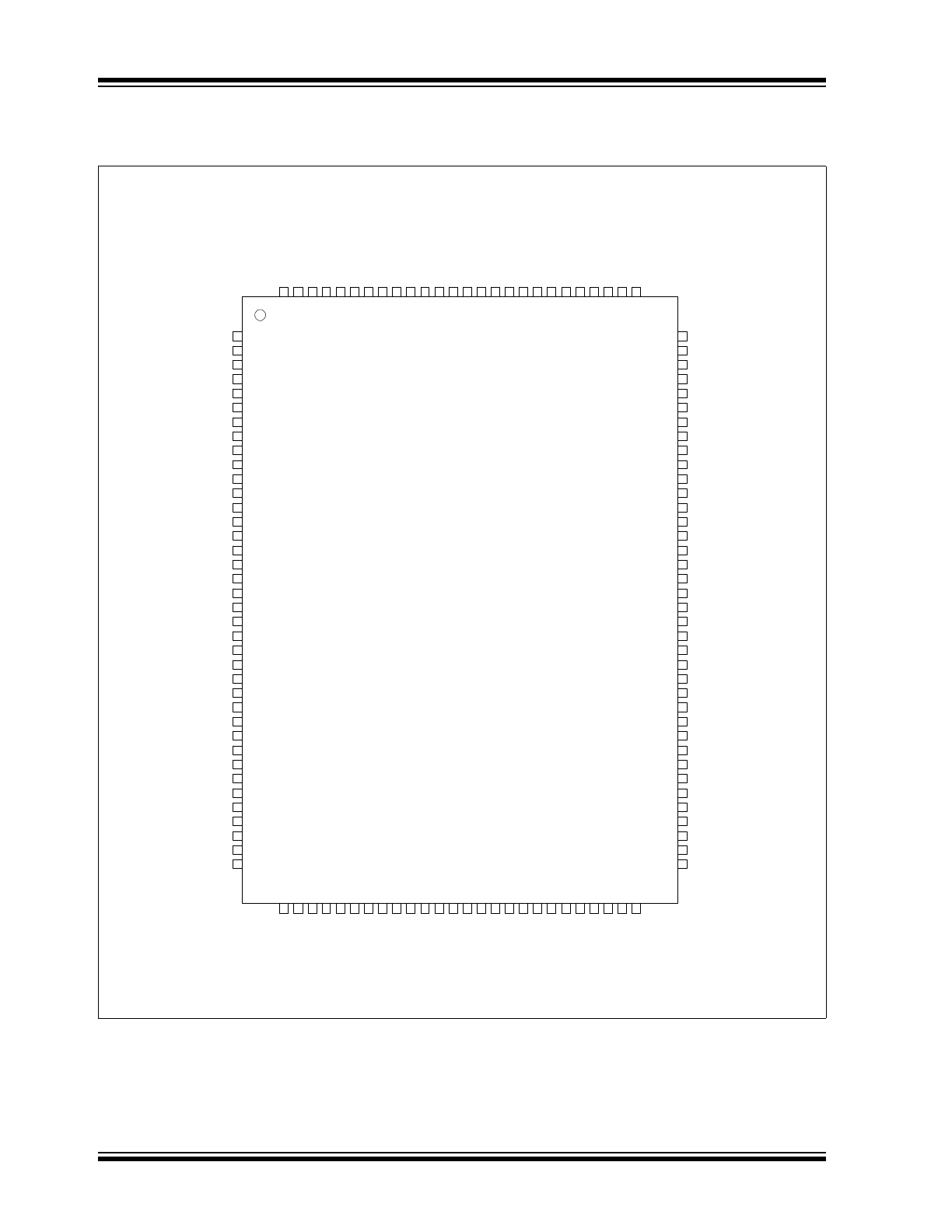
FIGURE 2-2:
PIN CONFIGURATION - LAN91C111-FEAST 128-PIN QFP
1
2
3
4
5
6
7
8
9
10
11
12
13
14
15
16
17
18
19
20
21
22
23
24
25
26
27
28
29
30
31
32
33
34
35
36
37
38
128
127
126
125
124
123
122
121
120
119
118
117
116
115
114
113
112
111
110
109
108
107
106
105
104
103
102
101
100
99
98
97
96
95
94
93
92
91
90
89
88
87
86
85
84
83
82
81
80
79
78
77
76
75
74
73
72
71
70
69
68
67
66
65
39
40
41
42
43
44
45
46
47
48
49
50
51
52
53
54
55
56
57
58
59
60
61
62
63
64
LAN91C111-
FEAST
TM
128 PIN QFP
XTAL1
XTAL2
VDD
nCSOUT
IOS0
IOS1
IOS2
ENEEP
EEDO
EEDI
EESK
EECS
AVDD
RBIAS
AGND
TPO+
TPO-
AVDD
TPI+
TPI-
AGND
nLNK
LBK
nLEDA
nLEDB
GND
MDI
MDO
MCLK
nCNTRL
INTR0
RESET
nRD
nWR
VDD
nDATACS
nCYCLE
W/nR
RX_ER
RX_DV
RXD0
RXD1
RXD2
RXD3
VDD
CRS100
RX25
GND
TXD0
TXD1
TXD2
TXD3
COL
100
TXEN100
VDD
TX2
5
GND
D0
D1
D2
D3
GND
D4
D5
D6
D7
VDD
nBE3
nBE2
nBE1
nBE0
GND
A15
A14
A13
A12
A11
A10
A9
A8
A7
A6
A5
A4
A3
A2
A1
VDD
D8
D9
D10
D11
GND
D12
D13
D14
D15
GND
D16
D17
D18
D19
nADS
ARDY
GND
nVLBUS
AEN
LCLK
nSRDY
VDD
nLDEV
nRDYRTN
X25OUT
D31
D30
D29
D28
GND
D27
D26
D25
D24
GND
D23
D22
D21
D20
VDD
2011-2016 Microchip Technology Inc.
DS00002276A-page 7
LAN91C111
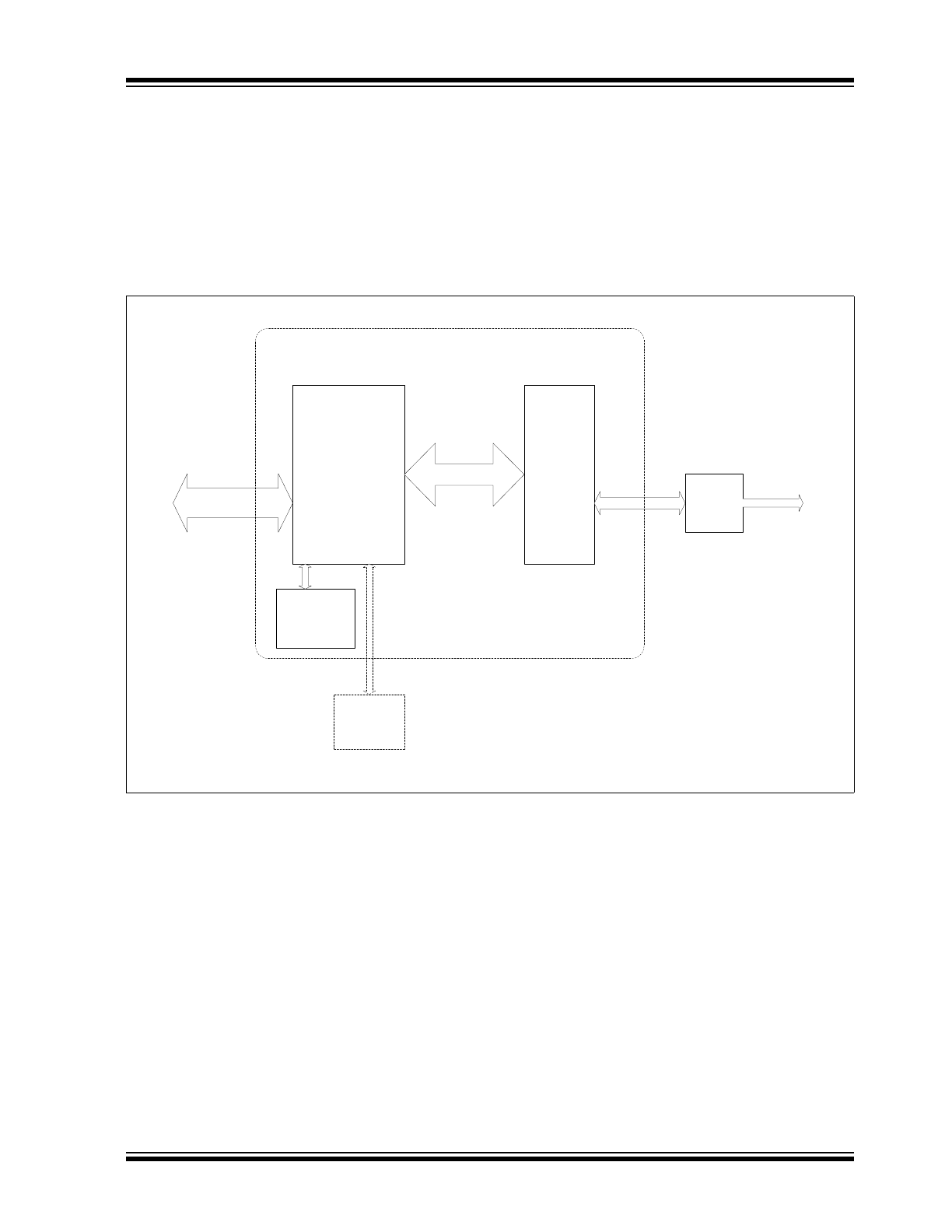
3.0
BLOCK DIAGRAMS
The diagram shown in
Figure 3-1, "Basic Functional Block Diagram"
, describes the device basic functional blocks. The
Microchip LAN91C111 is a single chip solution for embedded designs with minimal Host and external supporting devices
required to implement 10/100 Ethernet connectivity solutions.
The optional Serial EEPROM is used to store information relating to default IO offset parameters as well as which of the
Interrupt line are used by the host.
FIGURE 3-1:
BASIC FUNCTIONAL BLOCK DIAGRAM
PHY
Core
Ethernet
MAC
LAN91C111
Internal IEEE 802.3 MII (Media
Independent Interface)
Serial
EEProm
(Optional)
ISA,Embedded
Processor
Transformer
RJ45
Minimal LAN91C111
Configuration
Host System
TX/RX Buffer (8K)
LAN91C111
DS00002276A-page 8
2011-2016 Microchip Technology Inc.
The diagram shown in
Figure 3-2
describes the supported Host interfaces, which include ISA or Generic Embedded.
The Host interface is an 8, 16 or 32 bit wide address / data bus with extensions for 32, 16 and 8 bit embedded RISC
and ARM processors.
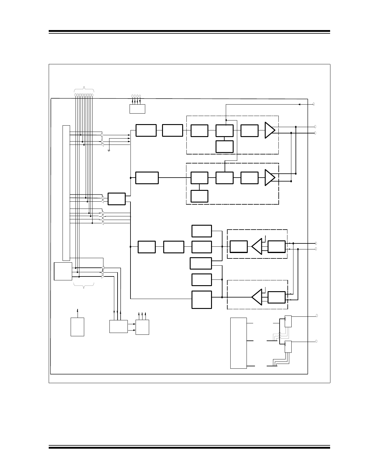
The figure shown next page describes the Microchip LAN91C111 functional blocks required to integrate a 10/100 Ether-
net Physical layer framer to the internal MAC.
FIGURE 3-2:
BLOCK DIAGRAM
8-32 bit
Bus
Interface
Unit
Arbiter
DMA
MMU
Ethernet
Protocol
Handler
(EPH)
10/100
PHY
8K Byte
Dynamically
Allocated
SRAM
WR
FIFO
RD
FIFO
Control
RX Data
TX Data
Control
Control
MII
Address
Data
Control
Control
RXD[0-3]
TXD[0-3]
Control
TX/RX
FIFO
Pointer
TPI
TPO
Control
EEPROM
INTERFACE
32-bit Data
32-bit Data
2011-2016 Microchip Technology Inc.
DS00002276A-page 9
LAN91C111
FIGURE 3-3:
LAN91C111 PHYSICAL LAYER TO INTERNAL MAC BLOCK DIAGRAM
COLLISION
4B5B
DECODER
DESCRAMBL
ER
CLOCK &
DATA
RECOVERY
AUTO
NEGOTIATION
& LINK
SQUELCH
CLOCK &
DATA
Recovery
(Manchester
Decoder)
LP
FILTER
ROM
DAC
+
-
10BASE-T
TRANSMITTER
CLOCK
GEN
(PLL)
MANCHESTER
4B5B
ENCODER
SCRAMBLER
TPO+
SWITCHED
CURRENT
SOURCE
+
-
100BASE-TX
TRANSMITTER
CLOCK
GEN
(PLL)
TPO-
LP
FILTER
TPI+
TPI-
LP
FILTER
+
-
+/- Vth
+
10BASE-T
RECEIVER
MLT3
ENCODER
ADAPTIVE
EQUALIZER
+
+/- Vth
+
100BASE-TX
RECEIVER
MLT
ENCODER
SQUELCH
RBIAS
CSM
A
/CD
S
1
S
8
D
C
1
EN
B
C
3
C
2
Multiplexer
S
1
S
8
D
C
1
EN
B
C
3
C
2
LS[2-0]B
LEDA
LEDB
nPLED[0-5]
LS[2-0]A
LED
Control
Power
On
Reset
PHY
CONTROLS
TXD[3:0]
TX_ER
TXEN100
TX25
CRS100
COL100
RXD[3:0]
RX_ER
RX_DV
RX25
MCLK
MDO
EE
CS
EE
SK
EED
O
To
M
II
E
x
ternal
S
ignals
MII
AUTONEG
LOGIC
EEPROM
CONTROL
MDI
MII
SERIAL
Manage
-ment
MII External
Signals
EED
I
Multiplexer
-

LAN91C111
DS00002276A-page 10
2011-2016 Microchip Technology Inc.
4.0
SIGNAL DESCRIPTIONS
TABLE 4-1:
LAN91C111 PIN REQUIREMENTS (128 PIN QFP AND 1.0MM TQFP PACKAGE)
Function
Pin Symbols
Number of Pins
System Address Bus
A1-A15, AEN, nBE0-nBE3
20
System Data Bus
D0-D31
32
System Control Bus
RESET, nADS, LCLK, ARDY,
nRDYRTN, nSRDY, INTR0, nLDEV,
nRD, nWR, nDATACS, nCYCLE, W/nR,
nVLBUS
14
Serial EEPROM
EEDI, EEDO, EECS, EESK, ENEEP,
IOS0-IOS2
8
LEDs
nLEDA, nLEDB
2
PHY
TPO+, TPO-, TPI+, TPI-, nLNK, LBK,
nCNTRL, RBIAS
8
Crystal Oscillator
XTAL1, XTAL2
2
Power
VDD, AVDD
10
Ground
GND, AGND
12
Physical Interface (MII)
TXEN100, CRS100, COL100, RX_DV,
RX_ER, TXD0-TXD3, RXD0-RXD3,
MDI, MDO, MCLK, RX25, TX25
18
MISC
nCSOUT, X25OUT
2
TOTAL
128