

SMSC LAN91C110 Rev. B
Page 1
Revision 1.0 (11-04-08)
DATASHEET
LAN91C110 REV. B
FEAST Fast Ethernet
Controller for
PCMCIA and Generic
16-Bit Applications
Product Features
Dual Speed CSMA/CD Engine (10 Mbps and 100
Mbps)
Compliant with IEEE 802.3 100BASE-T
Specification
Supports 100BASE-TX, 100BASE-T4
16 Bit Wide Data Path (into Packet Buffer Memory)
Generic 16-bit System Level Interface Easily
Adaptable to ISA, PCMCIA (16-bit CardBus), and
Various CPU System Interfaces
Support for 16 and 8 Bit CPU Accesses
Asynchronous Bus Interface
128 Kbyte External Memory
Built-in Transparent Arbitration for Slave Sequential
Access Architecture
Flat MMU Architecture with Symmetric Transmit
and Receive Structures and Queues
IEEE-802.3 MII (Media Independent Interface)
Compliant MAC-PHY Interface Running at Nibble
Rate
MII Management Serial Interface
IEEE-802.3u Full Duplex Capability
144 Pin TQFP lead-free RoHS Compliant package
(1.0 Millimeter Height)
ORDER NUMBER(S):
LAN91C110-PU for 144 pin TQFP lead-free RoHS Compliant package

FEAST Fast Ethernet Controller
for PCMCIA and Generic 16-Bit Applications
Datasheet
SMSC LAN91C110 Rev. B
Page 2
Revision 1.0 (11-04-08)
DATASHEET
80 ARKAY DRIVE, HAUPPAUGE, NY 11788 (631) 435-6000, FAX (631) 273-3123
Copyright © 2008 SMSC or its subsidiaries. All rights reserved.
Circuit diagrams and other information relating to SMSC products are included as a means of illustrating typical applications. Consequently, complete
information sufficient for construction purposes is not necessarily given. Although the information has been checked and is believed to be accurate, no
responsibility is assumed for inaccuracies. SMSC reserves the right to make changes to specifications and product descriptions at any time without
notice. Contact your local SMSC sales office to obtain the latest specifications before placing your product order. The provision of this information does
not convey to the purchaser of the described semiconductor devices any licenses under any patent rights or other intellectual property rights of SMSC
or others. All sales are expressly conditional on your agreement to the terms and conditions of the most recently dated version of SMSC's standard
Terms of Sale Agreement dated before the date of your order (the "Terms of Sale Agreement"). The product may contain design defects or errors
known as anomalies which may cause the product's functions to deviate from published specifications. Anomaly sheets are available upon request.
SMSC products are not designed, intended, authorized or warranted for use in any life support or other application where product failure could cause
or contribute to personal injury or severe property damage. Any and all such uses without prior written approval of an Officer of SMSC and further
testing and/or modification will be fully at the risk of the customer. Copies of this document or other SMSC literature, as well as the Terms of Sale
Agreement, may be obtained by visiting SMSC’s website at http://www.smsc.com. SMSC is a registered trademark of Standard Microsystems
Corporation (“SMSC”). Product names and company names are the trademarks of their respective holders.
SMSC DISCLAIMS AND EXCLUDES ANY AND ALL WARRANTIES, INCLUDING WITHOUT LIMITATION ANY AND ALL IMPLIED WARRANTIES
OF MERCHANTABILITY, FITNESS FOR A PARTICULAR PURPOSE, TITLE, AND AGAINST INFRINGEMENT AND THE LIKE, AND ANY AND
ALL WARRANTIES ARISING FROM ANY COURSE OF DEALING OR USAGE OF TRADE. IN NO EVENT SHALL SMSC BE LIABLE FOR ANY
DIRECT, INCIDENTAL, INDIRECT, SPECIAL, PUNITIVE, OR CONSEQUENTIAL DAMAGES; OR FOR LOST DATA, PROFITS, SAVINGS OR
REVENUES OF ANY KIND; REGARDLESS OF THE FORM OF ACTION, WHETHER BASED ON CONTRACT; TORT; NEGLIGENCE OF SMSC
OR OTHERS; STRICT LIABILITY; BREACH OF WARRANTY; OR OTHERWISE; WHETHER OR NOT ANY REMEDY OF BUYER IS HELD TO
HAVE FAILED OF ITS ESSENTIAL PURPOSE, AND WHETHER OR NOT SMSC HAS BEEN ADVISED OF THE POSSIBILITY OF SUCH
DAMAGES.

FEAST Fast Ethernet Controller
for PCMCIA and Generic 16-Bit Applications
Datasheet
SMSC LAN91C110 Rev. B
Page 3
Revision 1.0 (11-04-08)
DATASHEET
Table Of Contents
Chapter 1
General Description............................................................................................................................5
Chapter 2
Pin Configuration ...............................................................................................................................6
Chapter 3
Description of Pin Functions..............................................................................................................7
Chapter 4
Functional Description .....................................................................................................................11
4.1
Description of Blocks......................................................................................................................... 11
4.1.1
Clock Generator Block ................................................................................................................ 11
4.2
CSMA/CD Block ................................................................................................................................ 11
4.2.1
DMA Block .................................................................................................................................. 11
4.2.2
Arbiter Block................................................................................................................................ 11
4.2.3
MMU Block.................................................................................................................................. 12
4.2.4
BIU Block .................................................................................................................................... 12
4.2.5
MAC-PHY Interface Block .......................................................................................................... 12
4.2.6
MII Management Interface Block ................................................................................................ 13
Chapter 5
Data Structures and Registers .........................................................................................................15
5.1
Packet Format in Buffer Memory ...................................................................................................... 15
5.2
Typical Flow of Events for Transmit (Auto Release = 0)................................................................... 37
5.3
Typical Flow of Events for Transmit (Auto Release = 1)................................................................... 38
5.4
Typical Flow of Events for Receive ................................................................................................... 40
5.5
Memory Partitioning .......................................................................................................................... 46
5.6
Interrupt Generation .......................................................................................................................... 46
Chapter 6
Operational Description...................................................................................................................49
6.1
Maximum Guaranteed Ratings* ........................................................................................................ 49
6.2
DC Electrical Characteristics............................................................................................................. 49
Chapter 7
Timing Diagrams ..............................................................................................................................51
Chapter 8
Package Outline ................................................................................................................................56
List of Figures
Figure 2.1 – Pin Configuration ...................................................................................................................... 6
Figure 3.1 - LAN91C110 Block Diagram..................................................................................................... 10
Figure 3.2 - LAN91C110 System Diagram ................................................................................................. 10
Figure 4.1 - LAN91C110 Internal Block Diagram with Data Path ............................................................... 14
Figure 5.1 – Data Packet Format................................................................................................................ 15
Figure 5.2 – Interrupt Structure ................................................................................................................... 33
Figure 5.3 – Interrupt Service Routine ........................................................................................................ 41
Figure 5.4 - RX INTR .................................................................................................................................. 42
Figure 5.5 - TX INTR................................................................................................................................... 43
Figure 5.6 - TXEMPTY INTR (Assumes auto release option selected)...................................................... 44
Figure 5.7 - Drive Send and Allocate Routines........................................................................................... 45
Figure 5.8 – Interrupt Generation for Transmit, Receive, MMU.................................................................. 48
Figure 7.1 - Asynchronous Cycle - nADS=0 ............................................................................................... 51
Figure 7.2 - Asynchronous Cycle - USING nADS....................................................................................... 51
Figure 7.3 – Address Latching for All Modes .............................................................................................. 52

FEAST Fast Ethernet Controller
for PCMCIA and Generic 16-Bit Applications
Datasheet
SMSC LAN91C110 Rev. B
Page 4
Revision 1.0 (11-04-08)
DATASHEET
Figure 7.4 - SRAM Interface ....................................................................................................................... 53
Figure 7.5 - MII Interface............................................................................................................................. 55
Figure 8.1 - 144 Pin TQFP Package Outlines............................................................................................. 56
List of Tables
Table 5.1 - Internal I/O Space Mapping........................................................................................................ 18
Table 8.1 – 144 Pin TQFP Package Parameters ....................................................................................... 56

FEAST Fast Ethernet Controller
for PCMCIA and Generic 16-Bit Applications
Datasheet
SMSC LAN91C110 Rev. B
Page 5
Revision 1.0 (11-04-08)
DATASHEET
Chapter 1
General Description
The LAN91C110 is designed to facilitate the implementation of second generation Fast Ethernet PC Card
adapters and other non-PCI connectivity products. The LAN91C110 is a digital device that implements the
Media Access Control (MAC) portion of the CSMA/CD protocol at 10 and 100 Mbps, and couples it with a lean
and fast data and control path system architecture to ensure that the CPU to packet RAM data movement
does not cause a bottleneck at 100 Mbps.
The LAN91C110 implements a generic 16-bit host interface which is adaptable to a wide range of system
buses and CPUs. This makes the LAN91C110 ideal for 10/100 Fast Ethernet implementations in systems
based on system buses other than PCI.
Total memory size is 128 Kbytes, equivalent to a total chip storage (transmit plus receive) of 64 outstanding
packets. The LAN91C110 is software compatible with the LAN9000 family of products in the default mode and
can use existing LAN9000 drivers (ODI, IPX, and NDIS) with minor modifications in 16 and 32 bit Intel X86
based environments.
Memory management is handled using a unique patented MMU (Memory Management Unit) architecture
and an internal 32-bit wide data path. This I/O mapped architecture can sustain back-to-back frame
transmission and reception for superior data throughput and optimal performance. It also dynamically
allocates buffer memory in an efficient buffer utilization scheme, reducing software tasks and relieving the
host CPU from performing these housekeeping functions. The total memory size is 128 Kbytes (external),
equivalent to a total chip storage (transmit and receive) of 64 outstanding packets.
FEAST provides a flexible slave interface for easy connectivity with industry-standard buses. The host
interface is “ISA-like” and is easily adapted to a wide range of system and CPU buses such as ISA,
PCMCIA, etc.
An IEEE-802.3 compliant Media Independent Interface (MII) provided on the network side of the LAN91C110.
The MII interface allows the use of a wide range of MII compliant Physical Layer (PHY) devices to be used with
the LAN91C110. The LAN91C110 also provides an interface to the two-line MII serial management protocol.
FEAST Fast Ethernet Controller
for PCMCIA and Generic 16-Bit Applications
Datasheet
SMSC LAN91C110 Rev. B
Page 6
Revision 1.0 (11-04-08)
DATASHEET
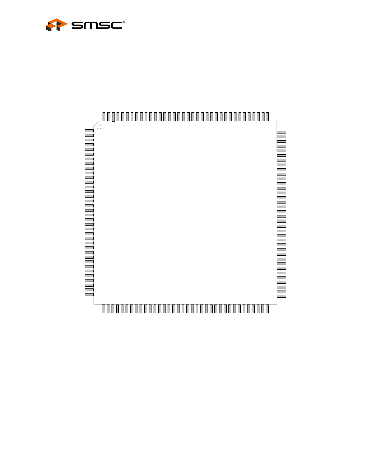
Chapter 2
Pin Configuration
LAN91C110
144 Pin TQFP
28
29
30
31
32
33
34
35
36
1
2
3
4
5
6
7
8
9
10
11
12
13
14
15
16
17
18
19
20
21
22
23
24
25
26
27
VDD
GND
XTAL2
XTAL1
VDD
nCSOUT
TX25
RX_ER
RX_DV
GND
RX25
COL100
CRS100
RXD0
RXD1
RXD2
RXD3
TXD0
TXD1
TXD2
TXD3
TXEN100
nRWE0
RD7
RD6
RD5
RD4
GND
RD3
RD2
RD1
VDD
RD0
RD15
RD14
nLNK
VDD
GND
RD8
RA1
2
RA4
RA3
GND
nR
W
E
3
RA2
RD2
4
RD2
5
RD2
6
RD2
7
RD2
8
RD2
9
nR
W
E
2
RD3
0
RD3
1
VDD
RD1
6
RD1
7
RD1
8
RD1
9
RD2
0
GND
RD2
1
RD2
2
RD2
3
RD1
3
RD1
2
GND
RD1
1
RD1
0
VDD
RD9
nR
W
E
1
45
46
47
48
49
50
51
52
53
54
55
56
57
58
59
60
61
62
63
64
65
66
67
68
69
70
71
72
37
38
39
40
41
42
43
44
A9
A8
A7
A6
A5
A4
A3
A2
A1
GND
D8
D9
VDD
D10
D11
D12
D13
D14
GND
D15
nADS
VDD
RA16
RA14
RA15
RA9
RA10
RA8
RA11
VDD
nROE
RA7
GND
RA13
RA5
RA6
108
107
106
105
104
103
102
101
100
99
98
97
96
95
94
93
92
91
90
89
73
74
75
76
77
78
79
80
81
82
83
84
85
86
87
88
nW
R
RESET
GND
MC
LK
AEN
AUI
SEL
MD
O
MD
I
AGND
N/C
AVDD
A1
0
VDD
nR
D
INT
0
GND
ARDY
D0
D1
D2
D3
GND
D4
D5
D6
nLD
E
V
D7
n
BE1
n
BE0
GND
A1
5
A1
4
A1
3
A1
2
VDD
A1
1
144
143
142
141
140
139
138
137
136
135
134
133
132
131
130
129
128
127
126
125
124
123
122
121
120
119
118
117
116
115
114
113
112
111
110
109
Figure 2.1 – Pin Configuration
FEAST Fast Ethernet Controller
for PCMCIA and Generic 16-Bit Applications
Datasheet
SMSC LAN91C110 Rev. B
Page 7
Revision 1.0 (11-04-08)
DATASHEET
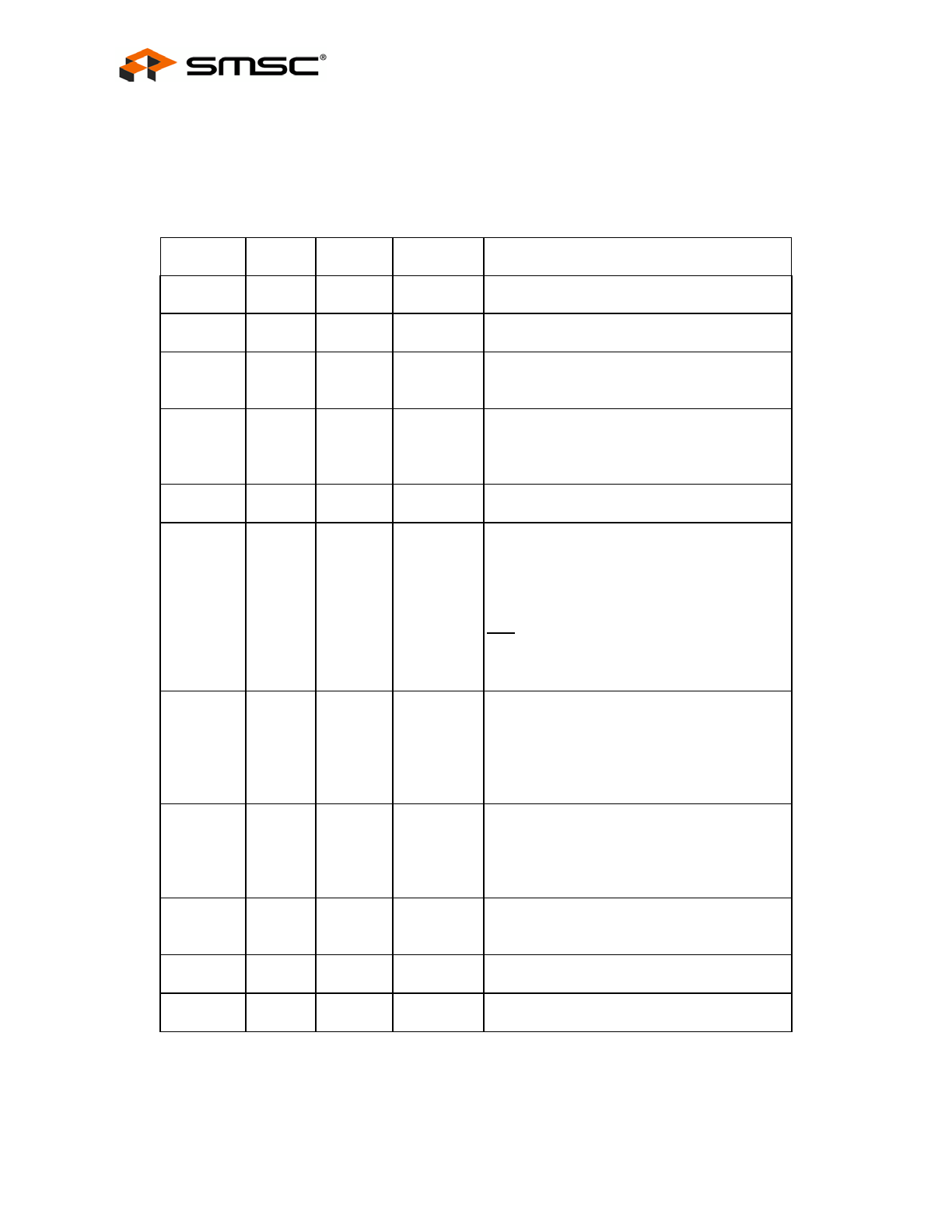
Chapter 3
Description of Pin Functions
144 TQFP
PIN NO.
NAME
SYMBOL
BUFFER
TYPE
DESCRIPTION
115-112,
110-100
Address
A[15:1]
I
Input. Used by LAN91C110 for internal register
selection.
138 Address
Enable
AEN
I
Input. Used as an address qualifier. Address
decoding is only enabled when AEN is low.
118, 117
nBE[1:0]
I
Input. Used during LAN91C110 register accesses
to determine the width of the access and the
register(s) being accessed.
89, 91-95,
97-98, 119,
121-123,
125-128
Data Bus D[15:0]
I/O8
Bidirectional. 16-bit data bus used to access the
LAN91C110’s internal registers. Data bus has
weak internal pullups. Supports direct connection
to the system bus without external buffering.
135
Reset
RESET
IS
Input. This input is not considered active unless it
is active for at least 100ns to filter narrow glitches.
129 Asynchro-
nous
Ready
ARDY
OD16
Open drain output. ARDY may be used when
interfacing asynchronous buses to extend
accesses. Its rising (access completion) edge is
controlled by the XTAL1 clock and, therefore,
asynchronous to the host CPU or bus clock.
Note: Asserted for 100 to 150ns for the
appropriate NO WAIT bit state in the Configuration
register. See the NO WAIT bit description for
complete information.
120 Local
Device
nLDEV
O16
Output. Local Device. This active low output is
asserted when AEN is low and A4-A15 decode to
the LAN91C110 address programmed into the
high byte of the Base Address Register. nLDEV*
is a combinatorial decode of unlatched address
and AEN signals.
88 nAddress
Strobe
nADS
IS
Input. Address strobe. For systems that require
address latching. The rising edge of nADS
indicates the latching moment of A[1:15] and AEN.
All LAN91C110 internal functions of A[1:15] and
AEN are latched.
131
Interrupt
INTR0
O4
Output. The interrupt output is enabled by
selecting the appropriate routing bits (INT SEL 1-
0) in the Configuration Register.
132 nRead
Strobe
nRD
IS
Input. Used in asynchronous bus interfaces.
134 nWrite
Strobe
nWR
IS
Input. Used in asynchronous bus interfaces.
FEAST Fast Ethernet Controller
for PCMCIA and Generic 16-Bit Applications
Datasheet
SMSC LAN91C110 Rev. B
Page 8
Revision 1.0 (11-04-08)
DATASHEET
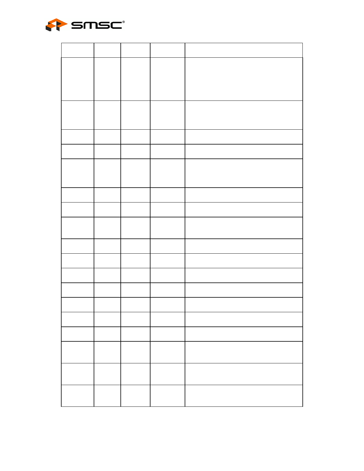
144 TQFP
PIN NO.
NAME
SYMBOL
BUFFER
TYPE
DESCRIPTION
56-57, 60-
65, 46-48,
50-54, 35-
38, 40-42,
45, 25-28,
30-32, 34
RAM Data
Bus
RD[31:0] I/O4
with
pullups
Bidirectional. Carries the local buffer memory
read and write data. Reads are always 32 bits
wide. Writes are controlled individually at the byte
level.
86,84,85,
75,72,80, 82-
83,81, 77,74-
73, 71-70,67
RAM
Address
Bus
RA[16:2]
O4
Outputs. This bus specifies the buffer RAM
doubleword being accessed by the LAN91C110.
78
nROE
O4
Output. Active low signal used to read a
doubleword from buffer RAM.
24,44,58, 68
nRWE[3:0]
O4
Outputs. Active low signals used to write any
byte, word or dword in RAM.
2
3
Crystal 1
Crystal 2
XTAL1
XTAL2
Iclk
An external 25 MHz crystal is connected across
these pins. If a TTL clock is supplied instead, it
should be connected to XTAL1 and XTAL2 should
be left open.
1 nLink
Status
nLNK
I with pullup Input. General purpose input port used to convey
LINK status (EPHSR bit 14).
139
AUI Select AUISEL
O4
Output. Non volatile output pin. Driven by AUI
SELECT (CONFIG bit 8).
23 Transmit
Enable
MII
TXEN100
O12
Output to MII PHY. Envelope to 100 Mbps
transmission.
12 Carrier
Sense MII
CRS100 I
with
pulldown
Input from MII PHY. Envelope of packet reception
used for deferral and backoff purposes.
8 Receive
Data Valid
RX_DV I
with
pulldown
Input from MII PHY. Envelope of data valid
reception. Used for receive data framing.
11 Collision
Detect MII
COL100 I
with
pulldown
Input from MII PHY. Collision detection input.
18,19,21, 22 Transmit
Data
TXD[3:0]
O12
Outputs. Transmit Data nibble to MII PHY.
6 Transmit
Clock
TX25
I with pullup Input. Transmit clock input from MII. Nibble rate
clock (25 MHz).
10 Receive
Clock
RX25
I with pullup Input. Receive clock input from MII PHY. Nibble
rate clock.
16-13 Receive
Data
RXD[3:0]
I
Inputs. Received Data nibble from MII PHY.
141 Manage-
ment Data
Input
MDI
I with
pulldown
MII management data input.
140 Manage-
ment Data
Output
MDO
O4
MII management data output.
137 Manage-
ment
Clock
MCLK O4
MII
management
clock.
FEAST Fast Ethernet Controller
for PCMCIA and Generic 16-Bit Applications
Datasheet
SMSC LAN91C110 Rev. B
Page 9
Revision 1.0 (11-04-08)
DATASHEET
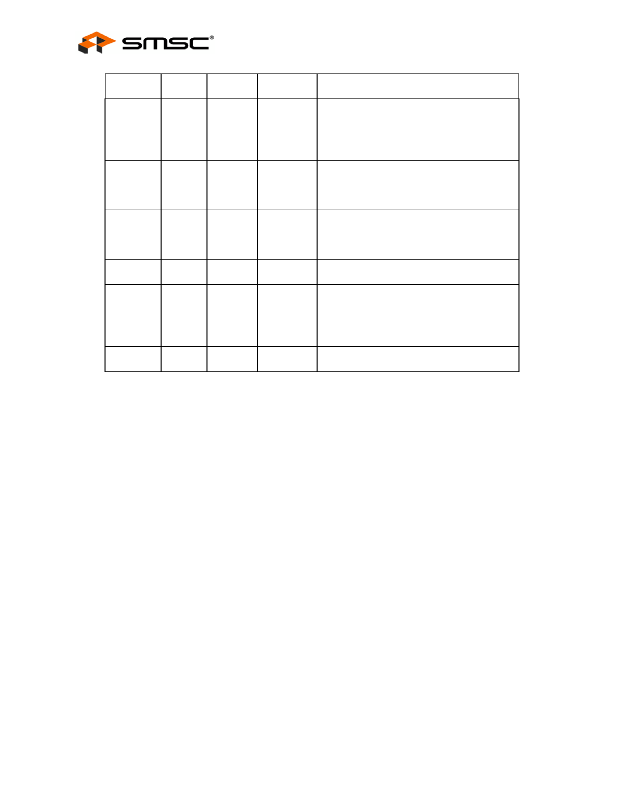
144 TQFP
PIN NO.
NAME
SYMBOL
BUFFER
TYPE
DESCRIPTION
7 Receive
Error
RX_ER I
with
pulldown
Input. Indicates a code error detected by PHY.
Used by the LAN91C110 to discard the packet
being received. The error indication reported for
this event is the same as a bad CRC (Receive
Status Word bit 13).
5 nChip
Select
Output
nCSOUT
O4
Output. Chip Select provided for mapping of PHY
functions into LAN91C110 decoded space. Active
on accesses to LAN91C110’s eight lower
addresses when the BANK SELECTED is 7.
4,20,33,43,5
5,66,79,
87,96,111,13
3
Power
VDD
+5V power supply pins.
144 Analog
Power
AVDD
+5V analog power supply pins.
9,17,29,39,4
9,59,69,
76,90,99,
116,124,
130,136,
Ground GND
Ground
pins.
142 Analog
Ground
AGND
Analog ground pin.
BUFFER TYPES
O4 O
UTPUT BUFFER WITH
2
M
A
SOURCE AND
4
M
A
SINK
O12
Output buffer with 6mA source and 12mA sink
OD16
Open drain buffer with 16mA sink
I/O4 Bidirectional
buffer with 2mA source and 4mA sink
I/O8 Bidirectional
buffer with 4mA source and 8mA sink
IS
Schmitt Trigger (Hysteresis: 250mV)
I with pullup
Rated at 30mA
I with pulldown
Rated at 30mA
FEAST Fast Ethernet Controller
for PCMCIA and Generic 16-Bit Applications
Datasheet
SMSC LAN91C110 Rev. B
Page 10
Revision 1.0 (11-04-08)
DATASHEET
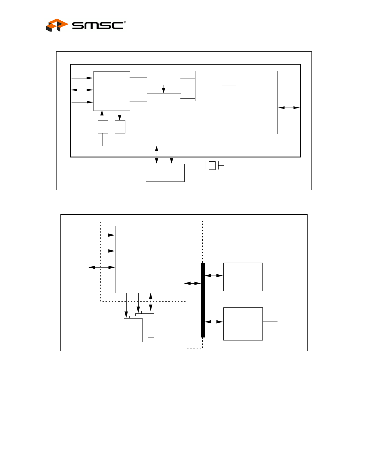
Figure 3.1 - LAN91C110 Block Diagram
Figure 3.2 - LAN91C110 System Diagram
ADDRESS
CONTROL
DATA
ADDRESS
CONTROL
DATA
SYSTEM BUS
MII
RD0-31
OE,WE
RA
SRAM
32kx8
1
2
3 4
LAN91C110
FEAST
100BASE-T4
INTERFACE
CHIP
100BASE-T4
100BASE-TX
INTERFACE
LOGIC/
10BASE-T
100BASE-TX/
10BASE-T
OR
BUS
INTERFACE
UNIT
ARBITER
MEMORY
MANAGEMENT
UNIT
DIRECT
MEMORY
ACCESS
MEDIA
ACCESS
CONTROL
RD
FIFO
WR
FIFO
Address
Data
Control
RAM
25 MHz
10/100 Mb/s
Media
Independent
Interface