

SMSC LAN91C100FD Rev. D
Page 1
Revision 1.0 (09-22-08)
DATASHEET
LAN91C100FD REV. D
FEAST Fast Ethernet
Controller with Full
Duplex Capability
Datasheet
Product Features
Dual Speed CSMA/CD Engine (10 Mbps and 100
Mbps)
Compliant with IEEE 802.3 100BASE-T
Specification
Supports 100BASE-TX, 100BASE-T4, and
10BASE-T Physical Interfaces
32 Bit Wide Data Path (into Packet Buffer
Memory)
Support for 32 and 16 Bit Buses
Support for 32, 16 and 8 Bit CPU Accesses
Synchronous, Asynchronous and Burst DMA
Interface Mode Options
128 Kbyte External Memory
Built-In Transparent Arbitration for Slave
Sequential Access Architecture
Flat MMU Architecture with Symmetric
Transmit and Receive Structures and
Queues
MII (Media Independent Interface) Compliant
MAC-PHY Interface Running at Nibble Rate
MII Management Serial Interface
Seven Wire Interface to 10 Mbps ENDEC
EEPROM-Based
Setup
Full Duplex Capability
ORDER NUMBER(S):
LAN91C100-FD for 208-pin QFP package
LAN91C100-FD-SS for 208-pin QFP lead-free RoHS compliant package
LAN91C100-FD for 208-pin TQFP package
LAN91C100-FD-ST for 208-pin TQFP lead-free RoHS compliant package

FEAST Fast Ethernet Controller with Full Duplex Capability
Revision 1.0 (09-22-08)
Page 2
SMSC LAN91C100FD Rev. D
DATASHEET
80 ARKAY DRIVE, HAUPPAUGE, NY 11788 (631) 435-6000, FAX (631) 273-3123
Copyright © 2008 SMSC or its subsidiaries. All rights reserved.
Circuit diagrams and other information relating to SMSC products are included as a means of illustrating typical applications. Consequently, complete
information sufficient for construction purposes is not necessarily given. Although the information has been checked and is believed to be accurate, no
responsibility is assumed for inaccuracies. SMSC reserves the right to make changes to specifications and product descriptions at any time without
notice. Contact your local SMSC sales office to obtain the latest specifications before placing your product order. The provision of this information does
not convey to the purchaser of the described semiconductor devices any licenses under any patent rights or other intellectual property rights of SMSC
or others. All sales are expressly conditional on your agreement to the terms and conditions of the most recently dated version of SMSC's standard
Terms of Sale Agreement dated before the date of your order (the "Terms of Sale Agreement"). The product may contain design defects or errors
known as anomalies which may cause the product's functions to deviate from published specifications. Anomaly sheets are available upon request.
SMSC products are not designed, intended, authorized or warranted for use in any life support or other application where product failure could cause
or contribute to personal injury or severe property damage. Any and all such uses without prior written approval of an Officer of SMSC and further
testing and/or modification will be fully at the risk of the customer. Copies of this document or other SMSC literature, as well as the Terms of Sale
Agreement, may be obtained by visiting SMSC’s website at http://www.smsc.com. SMSC is a registered trademark of Standard Microsystems
Corporation (“SMSC”). Product names and company names are the trademarks of their respective holders.
SMSC DISCLAIMS AND EXCLUDES ANY AND ALL WARRANTIES, INCLUDING WITHOUT LIMITATION ANY AND ALL IMPLIED WARRANTIES
OF MERCHANTABILITY, FITNESS FOR A PARTICULAR PURPOSE, TITLE, AND AGAINST INFRINGEMENT AND THE LIKE, AND ANY AND
ALL WARRANTIES ARISING FROM ANY COURSE OF DEALING OR USAGE OF TRADE. IN NO EVENT SHALL SMSC BE LIABLE FOR ANY
DIRECT, INCIDENTAL, INDIRECT, SPECIAL, PUNITIVE, OR CONSEQUENTIAL DAMAGES; OR FOR LOST DATA, PROFITS, SAVINGS OR
REVENUES OF ANY KIND; REGARDLESS OF THE FORM OF ACTION, WHETHER BASED ON CONTRACT; TORT; NEGLIGENCE OF SMSC
OR OTHERS; STRICT LIABILITY; BREACH OF WARRANTY; OR OTHERWISE; WHETHER OR NOT ANY REMEDY OF BUYER IS HELD TO
HAVE FAILED OF ITS ESSENTIAL PURPOSE, AND WHETHER OR NOT SMSC HAS BEEN ADVISED OF THE POSSIBILITY OF SUCH
DAMAGES.

FEAST Fast Ethernet Controller with Full Duplex Capability
SMSC LAN91C100FD Rev. D
Page 3
Revision 1.0 (09-22-08)
DATASHEET
Table Of Contents
Chapter 1
General Description ............................................................................................................. 5
Chapter 2
Pin Configuration................................................................................................................. 6
Chapter 3
Description of Pin Functions ............................................................................................... 7
Chapter 4
Functional Description....................................................................................................... 15
4.1
Description of Block........................................................................................................................... 15
4.1.1
Clock Generator Block............................................................................................................................15
4.2
CSMA/CD BLOCK............................................................................................................................. 15
4.2.1
DMA Block ..............................................................................................................................................15
4.2.2
Arbiter Block ...........................................................................................................................................15
4.2.3
MMU Block .............................................................................................................................................16
4.2.4
BIU Block ................................................................................................................................................16
4.2.5
MAC-PHY Interface Block ......................................................................................................................16
4.2.6
MII Management Interface Block ............................................................................................................17
4.2.7
Serial EEPROM Interface .......................................................................................................................17
Chapter 5
Data Structures and Registers .......................................................................................... 19
5.1
Packet Format in Buffer Memory ...................................................................................................... 19
5.2
Typical Flow of Events for Transmit (Auto Release = 0)................................................................... 41
5.3
Typical Flow of Events for Transmit (Auto Release = 1)................................................................... 42
5.4
Typical Flow of Events for Receive ................................................................................................... 43
5.5
Memory Partitioning .......................................................................................................................... 48
5.6
Interrupt Generation .......................................................................................................................... 49
Chapter 6
Board Setup Information .................................................................................................. 52
Chapter 7
Application Considerations ............................................................................................... 55
7.1
Fast Ethernet Slave Adapter ............................................................................................................. 55
7.2
VL Local Bus 32 Bit Systems ............................................................................................................ 55
7.3
High End ISA or Non-Burst EISA Machines...................................................................................... 58
7.4
EISA 32 Bit SLAVEEISA 32 Bit Slave............................................................................................... 60
Chapter 8
Operational Description .................................................................................................... 63
8.1
Maximum Guaranteed Ratings* ........................................................................................................ 63
8.2
DC Electrical Characteristics............................................................................................................. 63
Chapter 9
Timing Diagrams................................................................................................................ 66
Chapter 10
Package Outlines............................................................................................................. 76
List of Figures
Figure 3.1 - LAN91C100FD Block Diagram .................................................................................................................13
Figure 3.2 - LAN91C100FD System Diagram ..............................................................................................................14
Figure 4.1 - LAN91C100FD Internal Bock diagram with Data Path..............................................................................18
Figure 5.1 - Data Packet Format ..................................................................................................................................19
Figure 5.2 - Interrupt Structure .....................................................................................................................................37
Figure 5.3 - Interrupt Service Routine ..........................................................................................................................44
Figure 5.4 - RX INTR ...................................................................................................................................................45
Figure 5.5 - TX INTR....................................................................................................................................................46
Figure 5.6 - TXEMPTY INTR (Assumes Auto release Option Selected) ......................................................................47
Figure 5.7 - Drive Send and Allocate Routines ............................................................................................................48
Figure 5.8 - Interrupt Generation for Transmit, Receive, MMU ....................................................................................51
Figure 6.1 - 64 X 16 Serial EEPROM Map ...................................................................................................................54

FEAST Fast Ethernet Controller with Full Duplex Capability
Revision 1.0 (09-22-08)
Page 4
SMSC LAN91C100FD Rev. D
DATASHEET
Figure 7.1 - LAN91C100FD on VL BUS.......................................................................................................................57
Figure 7.2 - LAN91C100FD on ISA Bus.......................................................................................................................59
Figure 7.3 - LAN91C100FD on EISA Bus ....................................................................................................................62
Figure 9.1 - Asynchronous Cycle - nADS=0.................................................................................................................66
Figure 9.2 - Asynchronous Cycle - Using nADS...........................................................................................................67
Figure 9.3 - Asynchronous Cycle - nADS=0.................................................................................................................68
Figure 9.4 - Burst Write Cycles - nVLBUS=1 ...............................................................................................................69
Figure 9.5 - Burst Read Cycles - nVLBUS=1 ...............................................................................................................70
Figure 9.6 - Address Latching for all Modes.................................................................................................................71
Figure 9.7 - Synchronous Write Cycles - nVLBUS=0 ...................................................................................................71
Figure 9.8 - Synchronous Read Cycle - NVLBUS=0 ....................................................................................................72
Figure 9.9 - SRAM Interface ........................................................................................................................................73
Figure 9.10 - ENDEC Interface - 10 Mbps ...................................................................................................................74
Figure 9.11 - MII Interface............................................................................................................................................75
Figure 10.1 - 208 Pin QFP Package Outline ................................................................................................................76
Figure 10.2 - 208 Pin TQFP Package Outlines ............................................................................................................77
List of Tables
Table 3.1 - LAN91C100FD Pin Requirements
12
Table 5.1 - Internal I/O Space Mapping
22
Table 7.1 - VL Local Bus Signal Connections
55
Table 7.2 - High-End ISA or Non-Burst EISA Machines Signal Connectors
58
Table 7.3 - EISA 32 Bit Slave Signal Connections
60
Table 10.1 - 208 Pin QFP Package Parameters
76
Table 10.2 - 208 Pin TQFP Package Outlines
77

FEAST Fast Ethernet Controller with Full Duplex Capability
SMSC LAN91C100FD Rev. D
Page 5
Revision 1.0 (09-22-08)
DATASHEET
Chapter 1
General Description
The LAN91C100FD is designed to facilitate the implementation of first generation Fast Ethernet adapters
and connectivity products. For this first generation of products, flexibility dominates over integration. The
LAN91C100FD is a digital device that implements the MAC portion of the CSMA/CD protocol at 10 and
100 Mbps, and couples it with a lean and fast data and control path system architecture to ensure the CPU
to packet RAM data movement does not cause a bottleneck at 100 Mbps.
Total memory size is 128 Kbytes, equivalent to a total chip storage (transmit plus receive) of 64 outstanding
packets. The LAN91C100FD is software compatible with the LAN9000 family of products and can use existing
LAN9000 drivers (ODI, IPX, and NDIS) in 16 and 32 bit Intel X86 based environments.
Memory management is handled using a unique MMU (Memory Management Unit) architecture and a 32-
bit wide data path. This I/O mapped architecture can sustain back-to-back frame transmission and
reception for superior data throughput and optimal performance. It also dynamically allocates buffer
memory in an efficient buffer utilization scheme, reducing software tasks and relieving the host CPU from
performing these housekeeping functions. The total memory size is 128 Kbytes (external), equivalent to a
total chip storage (transmit and receive) of 64 outstanding packets.
FEAST provides a flexible slave interface for easy connectivity with industry-standard buses. The Bus
Interface Unit (BIU) can handle synchronous as well as asynchronous buses, with different signals being
used for each one. FEAST's bus interface supports synchronous buses like the VESA local bus, as well
as burst mode DMA for EISA environments. Asynchronous bus support for ISA is supported even though
ISA cannot sustain 100 Mbps traffic. Fast Ethernet could be adopted for ISA-based nodes on the basis of
the aggregate traffic benefits.
Two different interfaces are supported on the network side. The first is a conventional seven wire ENDEC
interface that connects to the LAN83C694 for 10BASE-T and coax 10 Mbps Ethernet networks. The second
interface follows the MII (Media Independent Interface) specification draft standard, consisting of 4 bit wide
data transfers at the nibble rate. This interface is applicable to 10 Mbps or 100 Mbps networks. Three of the
LAN91C100FD’s pins are used to interface to the two-line MII serial management protocol. Four I/O ports
(one input and three output pins) are provided for LAN83C694 configuration.
The LAN91C100FD is based on the LAN91C100 FEAST, functional revision G modified to add full duplex
capability. Also added is a software-controlled option to allow collisions to discard receive packets.
Previously, the LAN91C100 supported a “Diagnostic Full Duplex” mode. Under this mode the transmit
packet is looped internally and received by the MAC. This mode was enabled using the FDUPLX bit in the
TCR. In order to avoid confusion, the new, broader full duplex function of the LAN91C100FD is
designated as Switched Full Duplex, and the TCR bit enabling it is designated as SWFDUP. When the
LAN91C100FD is configured for SWFDUP, it’s transmit and receive paths will operate independently and
some CSMA/CD functions will be disabled. When the controller is not configured for SWFDUP it will follow
the CSMA/CD protocol.
FEAST Fast Ethernet Controller with Full Duplex Capability
Revision 1.0 (09-22-08)
Page 6
SMSC LAN91C100FD Rev. D
DATASHEET
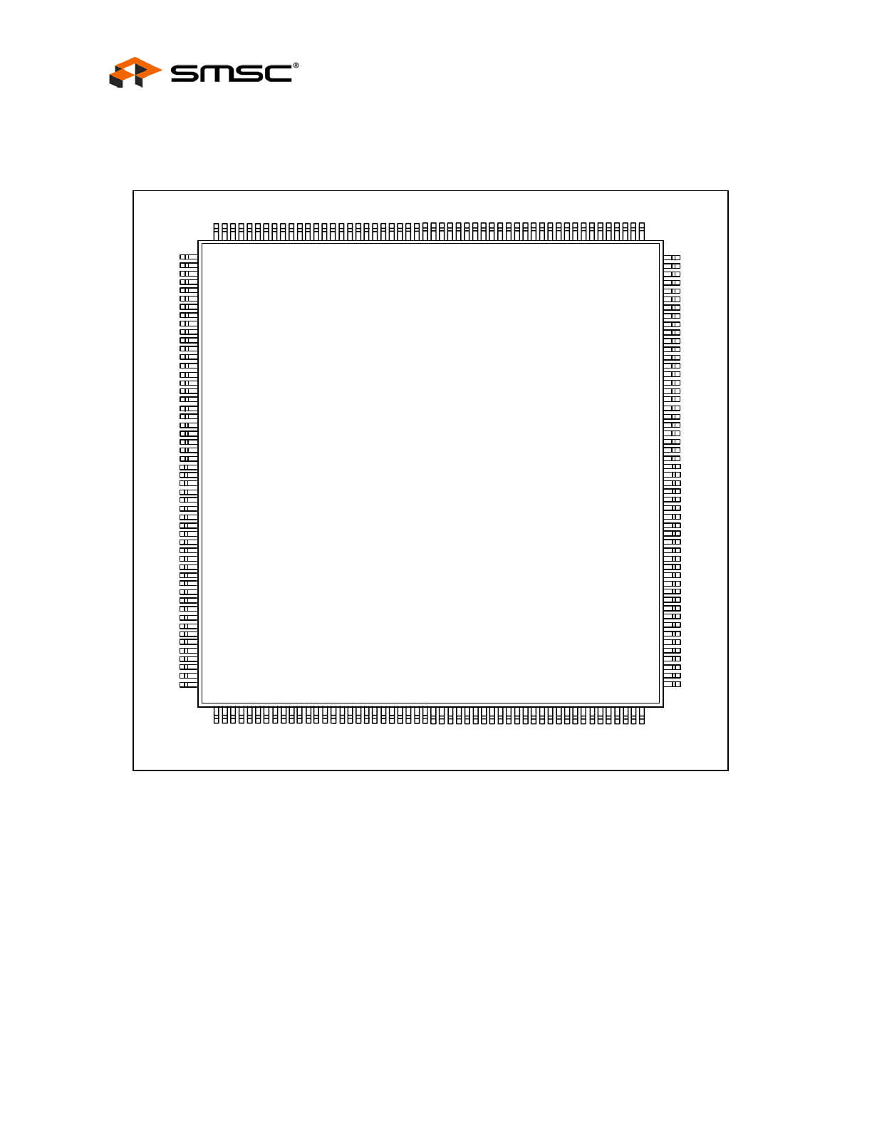
Chapter 2
Pin Configuration
LNK
TXEN
XTAL1
XTAL2
VDD
MIISEL
nCSOUT
nRXDISC
TX25
VDD
RX_ER
RX_DV
IOS0
GND
IOS1
IOS2
RX25
COL100
CRS100
RXD0
RXD1
RXD2
VDD
RXD3
TXD0
TXD1
VDD
TXD2
TXD3
TXEN100
nRWE0
GND
RD7
RD6
RD5
RD4
RDMAH
RD3
RD2
RD1
VDD
RD0
RD15
RD14
RD13
GND
RD12
RD11
RD10
GND
ENEEP
EEDO
1
2
3
4
5
6
7
8
9
10
11
12
13
14
15
16
17
18
19
20
21
22
23
24
25
26
27
28
29
30
31
32
33
34
35
36
37
38
39
40
41
42
43
44
45
46
47
48
49
50
51
52
A12
A11
A10
A9
A8
A7
A6
A5
A4
A3
A2
A1
D8
VDD
D9
D10
D11
D12
GND
D13
D14
D15
GND
D16
VDD
D17
D18
D19
GND
D20
D21
VDD
D22
D23
GND
D24
GND
VDD
D25
D26
GND
D27
D28
D29
D30
GND
D31
nRDYRTN
nLDEV
VDD
nSRDY
LCLK
156
155
154
153
152
151
150
149
148
147
146
145
144
143
142
141
140
139
138
137
136
135
134
133
132
131
130
129
128
127
126
125
124
123
122
121
120
119
118
117
116
115
114
113
112
111
110
109
108
107
106
105
CRS
CO
L
RX
D
AV
D
D
NC
AG
N
D
LB
K
TX
D
GN
D
RX
C
MD
I
TX
C
MD
O
nFSTEP
AU
IS
E
L
AE
N
MC
L
K
VD
D
nD
A
TA
C
S
IN
T
R
3
IN
T
R
2
IN
T
R
1
VD
D
GN
D
W/
nR
nC
Y
C
L
E
RE
S
E
T
nV
LBU
S
GN
D
VD
D
nWR
nR
D
IN
T
R
0
AR
D
Y
GN
D
D0
D1
D2
D3
GN
D
D4
D5
D6
VD
D
D7
nBE3
nB
E
2
nB
E1
nB
E0
A15
A1
4
A1
3
20
8
20
7
20
6
20
5
20
4
20
3
20
2
20
1
20
0
19
9
198
19
7
19
6
19
5
194
19
3
19
2
19
1
19
0
18
9
18
8
18
7
18
6
18
5
18
4
18
3
18
2
18
1
18
0
17
9
17
8
17
7
17
6
17
5
17
4
17
3
17
2
17
1
17
0
16
9
16
8
167
16
6
16
5
16
4
16
3
16
2
16
1
16
0
15
9
15
8
15
7
LAN91C100FD
208 Pin PQFP
and TQFP
53
54
55
56
57
58
59
60
61
62
63
64
65
66
67
68
69
70
71
72
73
74
75
76
77
78
79
80
81
82
83
84
85
86
87
88
89
90
91
92
93
94
95
96
97
98
99
100
101
102
103
104
EEDI
EE
SK
EEC
S
RD9
nR
WE1
NC
RD
8
RD23
RD
2
2
RD
2
1
VD
D
RD
20
RD
1
9
GN
D
RD
18
RD17
RD
1
6
RD
31
RD
30
NC
nR
WE2
VD
D
GN
D
RD2
9
RD
2
8
RD
27
RD
26
RD25
RD
2
4
GN
D
VD
D
RA
2
VD
D
nR
WE
3
RA3
RA4
RA
1
2
RA
5
RA6
RA13
RC
V
D
MA
GN
D
nADS
RA
7
nR
O
E
RA
11
RA8
RA
1
0
RA
9
RA
15
RA1
4
RA
1
6
LAN91C100FD
208 Pin QFP
and TQFP

FEAST Fast Ethernet Controller with Full Duplex Capability
SMSC LAN91C100FD Rev. D
Page 7
Revision 1.0 (09-22-08)
DATASHEET
Chapter 3
Description of Pin Functions
PQFP/TQFP
PIN NO.
NAME SYMBOL
BUFFER
TYPE
DESCRIPTION
148-159 Address A4-A15
I
Input. Decoded by LAN91C100FD to determine
access to its registers.
145-147 Address A1-A3
I
Input. Used by LAN91C100FD for internal
register selection.
193
Address
Enable
AEN I
Input. Used as an address qualifier. Address
decoding is only enabled when AEN is low.
160-163
nByte
Enable
nBE0-
nBE3
I
Input. Used during LAN91C100FD register
accesses to determine the width of the access
and the register(s) being accessed. nBE0-nBE3
are ignored when nDATACS is low (burst
accesses) because 32 bit transfers are
assumed.
173-170,
168-166,
164, 144,
142-139,
137-135,
133,
131-129,
127, 126,
124, 123,
121, 118,
117,
115-112,
110
Data Bus
D0-D31
I/O24
Bidirectional. 32 bit data bus used to access the
LAN91C100FD’s internal registers. Data bus
has weak internal pullups. Supports direct
connection to the system bus without external
buffering. For 16 bit systems, only D0-D15 are
used.
182 Reset RESET
IS Input. This input is not considered active unless
it is active for at least 100ns to filter narrow
glitches.
95
nAddress
Strobe
nADS IS
Input. For systems that require address latching,
the rising edge of nADS indicates the latching
moment for A1-A15 and AEN. All
LAN91C100FD internal functions of A1-A15,
AEN are latched except for nLDEV decoding.
183 nCycle nCYCLE
I Input. This active low signal is used to control
LAN91C100FD EISA burst mode synchronous
bus cycles.
184 Write/
nRead
W/nR IS
Input. Defines the direction of synchronous
cycles. Write cycles when high, read cycles
when low.
181
nVL Bus
Access
nVLBUS
I with
pullup
Input. When low, the LAN91C100FD
synchronous bus interface is configured for VL
Bus accesses. Otherwise, the LAN91C100FD is
configured for EISA DMA burst accesses. Does
not affect the asynchronous bus interface.
105
Local Bus
Clock
LCLK I
Input. Used to interface synchronous buses.
Maximum frequency is 50 MHz. Limited to 8.33
MHz for EISA DMA burst mode.

FEAST Fast Ethernet Controller with Full Duplex Capability
Revision 1.0 (09-22-08)
Page 8
SMSC LAN91C100FD Rev. D
DATASHEET
PQFP/TQFP
PIN NO.
NAME SYMBOL
BUFFER
TYPE
DESCRIPTION
175
Asynchron-
ous Ready
ARDY OD16
Open drain output. ARDY may be used when
interfacing asynchronous buses to extend
accesses. Its rising (access completion) edge is
controlled by the XTAL1 clock and, therefore,
asynchronous to the host CPU or bus clock.
106
nSynchron
-
ous Ready
nSRDY O16
Output. This output is used when interfacing
synchronous buses and nVLBUS=0 to extend
accesses. This signal remains normally inactive,
and its falling edge indicates completion. This
signal is synchronous to the bus clock LCLK.
109
nReady
Return
nRDYRTN I Input. This input is used to complete
synchronous read cycles. In EISA burst mode it
is sampled on falling LCLK edges, and
synchronous cycles are delayed until it is
sampled high.
176,
187-189
Interrupt
INTR0-
INTR3
O24
Outputs. Only one of these interrupts is selected
to be used; the other three are tri-stated. The
selection is determined by the value of INT SEL
1-0 bits in the Configuration Register.
108
nLocal
Device
nLDEV O16
Output. This active low output is asserted when
AEN is low and A4-A15 decode to the
LAN91C100FD address programmed into the
high byte of the Base Address Register. nLDEV
is a combinatorial decode of unlatched address
and AEN signals.
177
nRead
Strobe
nRD
IS
Input. Used in asynchronous bus interfaces.
178
nWrite
Strobe
nWR
IS
Input. Used in asynchronous bus interfaces.
190
nData
Path Chip
Select
nDATACS
I with
pullup
Input. When nDATACS is low, the Data Path
can be accessed regardless of the values of
AEN, A1-A15 and the content of the BANK
SELECT Register. nDATACS provides an
interface for bursting to and from the
LAN91C100FD 32 bits at a time.
54
EEPROM
Clock
EESK O4
Output. 4
μsec clock used to shift data in and
out of the serial EEPROM.
55
EEPROM
Select
EECS O4
Output. Serial EEPROM chip select. Used for
selection and command framing of the serial
EEPROM.
52
EEPROM
Data Out
EEDO O4
Output. Connected to the DI input of the serial
EEPROM.
53
EEPROM
Data In
EEDI
I with
pulldown
Input. Connected to the DO output of the serial
EEPROM.
13, 15, 16
I/O Base
IOS0-
IOS2
I with
pullup
Input. External switches can be connected to
these lines to select between predefined
EEPROM configurations.
51
Enable
EEPROM
ENEEP
I with
pullup
Input. Enables (when high or open)
LAN91C100FD accesses to the serial EEPROM.
Must be grounded if no EEPROM is connected
to the LAN91C100FD.

FEAST Fast Ethernet Controller with Full Duplex Capability
SMSC LAN91C100FD Rev. D
Page 9
Revision 1.0 (09-22-08)
DATASHEET
PQFP/TQFP
PIN NO.
NAME SYMBOL
BUFFER
TYPE
DESCRIPTION
42, 40-38,
36-33
RAM Data
Bus
RD0-RD7
I/O4 with
pullups
Bidirectional. Carries the local buffer memory
read and write data. Reads are always 32 bits
wide. Writes are controlled individually at the
byte level. Floated if FLTST=1 during RECEIVE
FRAME STATUS WORD writes for packet
forwarding information (RA2-RA16=0,
RCVDMA=1, nRWE0-nRWE3=0).
59, 56,
49-47,
45-43,
69-67, 65,
64, 62-60,
81-76, 71,
70
RAM Data
Bus
RD8-
RD31
I/O4 with
pullups
Bidirectional. Carries the local buffer memory
read and write data. Reads are always 32 bits
wide. Writes are controlled individually at the
byte level.
84, 87, 88,
90, 91, 96,
99, 101,
100, 98, 89,
92, 103,
102, 104
RAM
Address
Bus
RA2-RA16 O4 Outputs. This bus specifies the buffer RAM
doubleword being accessed by the
LAN91C100FD.
97
nROE
O4
Output. Active low signal used to read a
doubleword from buffer RAM.
31, 57, 73,
86
nRWE0-
RWE3
O4
Outputs. Active low signals used to write any
byte, word or dword in RAM.
93
Receive
DMA
RCVDMA O4
Output. This pin is active during LAN91C100FD
write memory cycles of receive packets.
3
4
Crystal 1
Crystal 2
XTAL1
XTAL2
Iclk
An external 25 MHz crystal is connected across
these pins. If a TTL clock is supplied instead, it
should be connected to XTAL1 and XTAL2
should be left open.
5, 10, 23,
27, 41, 63,
74, 83, 85,
107, 119,
125, 132,
143, 165,
179, 186,
191
Power
VDD
+5V power supply pins.
205
Analog
Power
AVDD
+5V analog power supply pins.
14, 32, 46,
50, 66, 75,
82, 94, 111,
116, 120,
122, 128,
134, 138,
169, 174,
180, 185,
200
Ground GND
Ground
pins.
203
Analog
Ground
AGND
Analog ground pin.
2
Transmit
Enable
TXEN O4
Output. Used for 10 Mbps ENDEC. This pin
stays low when MIISEL is high.

FEAST Fast Ethernet Controller with Full Duplex Capability
Revision 1.0 (09-22-08)
Page 10
SMSC LAN91C100FD Rev. D
DATASHEET
PQFP/TQFP
PIN NO.
NAME SYMBOL
BUFFER
TYPE
DESCRIPTION
201
Transmit
Data
TXD O4
Output. NRZ Transmit Data for 10 Mbps
ENDEC interface.
208
Carrier
Sense
CRS
I with
pulldown
Input. Carrier sense from 10 Mbps ENDEC
interface. This pin is ignored when MIISEL is
high.
207
Collision
Detect
COL
I with
pulldown
Input. Collision detection indication from 10
Mbps ENDEC interface. This pin is ignored
when MIISEL is high.
206
Receive
Data
RXD
I with
pullup
Input. NRZ Receive Data from 10 Mbps ENDEC
interface. This pin is ignored when MIISEL is
high.
197
Transmit
Clock
TXC
I with
pullup
Input. 10 MHz transmit clock used in 10 Mbps
operation. This pin is ignored when MIISEL is
high.
199
Receive
Clock
RXC
I with
pullup
Input. 10 MHz receive clock recovered by the 10
Mbps ENDEC. This pin is ignored when MIISEL
is high.
202 Loopback
LBK
O4
Output. Active when LOOP bit is set (TCR bit 1).
Independent of port selection (MIISEL=X).
1
nLink
Status
nLNK
I with
pullup
Input. General purpose input port used to
convey LINK status (EPHSR bit 14).
Independent of port selection (MIISEL=X).
195 nFullstep
nFSTEP O4
Output. Non volatile output pin. Driven by
inverse of FULLSTEP (CONFIG bit 10).
Independent of port selection (MIISEL=X).
6 MII
Select
MIISEL O4
Output. Non volatile output pin. Driven by MII
SELECT (CONFIG bit 15). High indicates the
MII port is selected, low indicates the 10 Mbps
ENDEC is selected.
194 AUI
Select
AUISEL O4
Output. Non volatile output pin. Driven by AUI
SELECT (CONFIG bit 8). Independent of port
selection (MIISEL= X).
30
Transmit
Enable
100 Mbps
TXEN100 O12
Output to MII PHY. Envelope to 100 Mbps
transmission. This pin stays low if MIISEL is low.
19
Carrier
Sense 100
Mbps
CRS100
I with
pulldown
Input from MII PHY. Envelope of packet
reception used for deferral and backoff
purposes. This pin is ignored when MIISEL is
low.
12
Receive
Data Valid
RX_DV
I with
pulldown
Input from MII PHY. Envelope of data valid
reception. Used for receive data framing. This
pin is ignored when MIISEL is low.
18
Collision
Detect
100 Mbps
COL100
I with
pulldown
Input from MII PHY. Collision detection input.
This pin is ignored when MIISEL is low.
25, 26, 28,
29
Transmit
Data
TXD0-
TXD3
O12
Outputs. Transmit Data nibble to MII PHY.
9
Transmit
Clock
TX25
I with
pullup
Input. Transmit clock input from MII. Nibble rate
clock (25 MHz). This pin is ignored when
MIISEL is low.
17
Receive
Clock
RX25
I with
pullup
Input. Receive clock input from MII PHY. Nibble
rate clock. This pin is ignored when MIISEL is
low.