

2009-2018 Microchip Technology Inc.
DS00001871D-page 1
Highlights
• Single-Chip Ethernet Physical Layer Transceiver
(PHY)
• Compliant with IEEE 802.3ab (1000BASE-T),
IEEE 802.3u (Fast Ethernet), and ISO 802-3/IEEE
802.3 (10BASE-T)
• HP Auto-MDIX support in accordance with IEEE
802.3ab specification at 10/100/1000 Mbps oper-
ation
• Miniature 56-pin QFN lead-free RoHS compliant
package with RGMII (8 x 8 x 0.85 mm height)
• Implements Reduced Power Operating Modes
Target Applications
• Set-Top Boxes
• Networked Printers and Servers
• Test Instrumentation
• LAN on Motherboard
• Embedded Telecom Applications
• Video Record/Playback Systems
• Cable Modems/Routers
• DSL Modems/Routers
• Digital Video Recorders
• IP and Video Phones
• Wireless Access Points
• Digital Televisions
• Digital Media Adapters/Servers
• Gaming Consoles
• POE Applications
Key Benefits
• High-Performance 10/100/1000 Ethernet Trans-
ceiver
- Compliant with IEEE 802.3ab (1000BASE-T)
- Compliant with IEEE 802.3/802.3u (Fast
Ethernet)
- Compliant with ISO 802-3/IEEE 802.3
(10BASE-T)
- 10BASE-T, 100BASE-TX and 1000BASE-T
support
- Loop-back modes
- Auto-negotiation (NEXT page support)
- Automatic polarity detection and correction
- Link status change wake-up detection
- Vendor specific register functions
- Supports reduced pin count RGMII interface
- Controlled impedance outputs
- Supports RGMII ID mode
- Three status LED outputs
- Compliant with IEEE 802.3-2005 standards
- RGMII pins tolerant to 3.6V
- Integrated DSP implements adaptive equal-
izer, echo cancelers, and crosstalk cancelers
- Efficient digital baseline wander correction
• Power and I/Os
- Various low power modes
- 2.5V I/O supply
• Miscellaneous Features
- IEEE 1149.1 (JTAG) boundary scan
- Multiple clock options - 25MHz crystal or
25MHz single-ended clock
• Packaging
- 56-pin QFN (8x8 mm) RoHS compliant pack-
age with RGMII
• Environmental
- Commercial temperature range
(0°C to +70°C)
- Industrial temperature range (-40°C to
+85°C)
LAN8820/LAN8820i
RGMII 10/100/1000 Ethernet Transceiver
with HP Auto-MDIX Support

LAN8820/LAN8820i
DS00001871D-page 2
2009-2018 Microchip Technology Inc.
TO OUR VALUED CUSTOMERS
It is our intention to provide our valued customers with the best documentation possible to ensure successful use of your Microchip
products. To this end, we will continue to improve our publications to better suit your needs. Our publications will be refined and
enhanced as new volumes and updates are introduced.
If you have any questions or comments regarding this publication, please contact the Marketing Communications Department via
E-mail at
docerrors@microchip.com
. We welcome your feedback.
Most Current Data Sheet
To obtain the most up-to-date version of this data sheet, please register at our Worldwide Web site at:
http://www.microchip.com
You can determine the version of a data sheet by examining its literature number found on the bottom outside corner of any page.
The last character of the literature number is the version number, (e.g., DS30000000A is version A of document DS30000000).
Errata
An errata sheet, describing minor operational differences from the data sheet and recommended workarounds, may exist for cur-
rent devices. As device/documentation issues become known to us, we will publish an errata sheet. The errata will specify the
revision of silicon and revision of document to which it applies.
To determine if an errata sheet exists for a particular device, please check with one of the following:
• Microchip’s Worldwide Web site;
http://www.microchip.com
• Your local Microchip sales office (see last page)
When contacting a sales office, please specify which device, revision of silicon and data sheet (include -literature number) you are
using.
Customer Notification System
Register on our web site at
www.microchip.com
to receive the most current information on all of our products.

2009-2018 Microchip Technology Inc.
DS00001871D-page 3
LAN8820/LAN8820i
Table of Contents
1.0 Introduction ..................................................................................................................................................................................... 4
2.0 Pin Description and Configuration .................................................................................................................................................. 5
3.0 Functional Description .................................................................................................................................................................. 13
4.0 Register Descriptions .................................................................................................................................................................... 34
5.0 Operational Characteristics ........................................................................................................................................................... 60
6.0 Package Outline ............................................................................................................................................................................ 76
Appendix A: Data Sheet Revision History ........................................................................................................................................... 78
The Microchip Web Site ...................................................................................................................................................................... 81
Customer Change Notification Service ............................................................................................................................................... 81
Customer Support ............................................................................................................................................................................... 81
Product Identification System ............................................................................................................................................................. 82
LAN8820/LAN8820i
DS00001871D-page 4
2009-2018 Microchip Technology Inc.
1.0
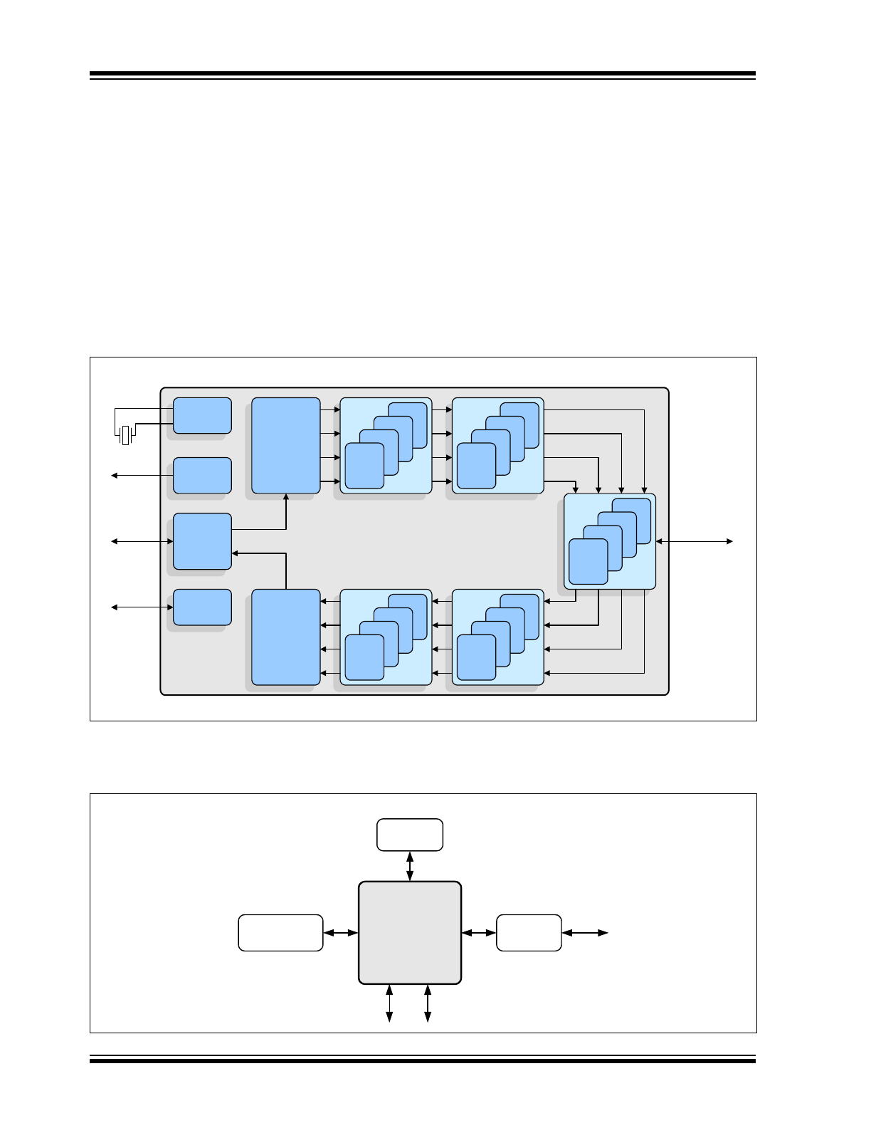
INTRODUCTION
The LAN8820/LAN8820i is a low-power 10BASE-T/100BASE-TX/1000BASE-T Gigabit Ethernet physical layer (PHY)
transceiver that is fully compliant with the IEEE 802.3 and 802.3ab standards.
The LAN8820/LAN8820i can be configured to communicate with an Ethernet MAC via the standard RGMII interface. It
contains a full-duplex transceiver for 1000 Mbps operation on four pairs of category 5 or better balanced twisted pair
cable. Per IEEE 802.3-2005 standards, all digital interface pins are tolerant to 3.6V.
The LAN8820/LAN8820i is configurable via hardware and software, supporting both IEEE 802.3-2005 compliant and
vendor-specific register functions via SMI. The LAN8820/LAN8820i implements Auto-Negotiation to automatically
determine the best possible speed and duplex mode of operation. HP Auto-MDIX support allows the use of direct con-
nect or crossover cables.
An internal block diagram of the LAN8820/LAN8820i is shown in
Figure 1-1
. A typical system-level diagram is shown in
Figure 1-2
.
FIGURE 1-1:
INTERNAL BLOCK DIAGRAM
FIGURE 1-2:
SYSTEM LEVEL BLOCK DIAGRAM
LAN8820/LAN8820i
RGMII
3
2
1
Active
Hybrid
0
10/100/1000
Ethernet
3
2
1
Analog
RX
0
3
2
1
Analog
TX
0
3
2
1
DSP
0
3
2
1
Spectral
Shaper
0
Digital TX
Scrambler
Trellis
4DPAM-5 Encoders
Digital RX
Descrambler
Viterbi Decoder
4DPAM-5 Decoders
3
2
1
0
3
2
1
0
3
2
1
0
3
2
1
0
Physical
Coding
Sublayer
TAP
Controller
LEDs
PLL
LEDs
JTAG
3
2
1
0
3
2
1
0
LAN8820/
LAN8820i
10/100/1000
Ethernet MAC
LED
Status
RGMII
Crystal
MDI
Ethernet
Magnetics
JTAG
Ethernet
2009-2018 Microchip Technology Inc.
DS00001871D-page 5
LAN8820/LAN8820i
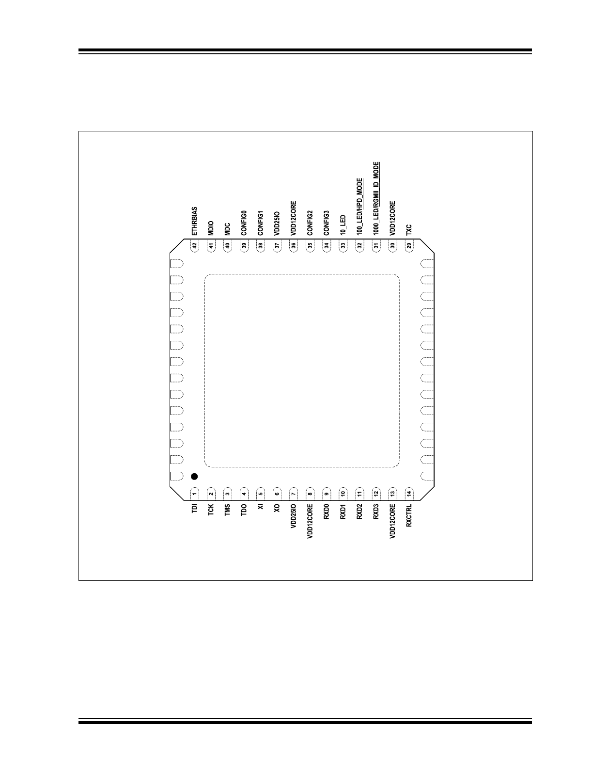
2.0
PIN DESCRIPTION AND CONFIGURATION
FIGURE 2-1:
56-QFN PIN ASSIGNMENTS (TOP VIEW)
VSS
NOTE: Exposed pad (VSS) on bottom of package must be connected to ground
LAN8820/LAN8820i
56 PIN QFN
(TOP VIEW)
TR0N
TXCTRL
15
16
17
18
19
20
21
22
23
24
25
26
27
28
56
55
54
53
52
51
50
49
48
47
46
45
44
43
TR0P
VDD12A
TR1N
TR1P
VDD12A
VDD12BIAS
VDD12PLL
TR2N
TR2P
VDD12A
TR3N
TR3P
VDD12A
TXD0
TXD1
TXD2
VDD25IO
VDD12CORE
TXD3
NC
VDD12CORE
VDD25IO
RXC
IRQ
nRESET
HPD

LAN8820/LAN8820i
DS00001871D-page 6
2009-2018 Microchip Technology Inc.
Note 2-1
Configuration strap values are latched on hardware reset. Configuration straps are identified by an
underlined symbol name. Signals that function as configuration straps must be augmented with an
external resistor when connected to a load. Refer to
Section 3.8, "Configuration," on page 23
for
additional information.
TABLE 2-1:
RGMII INTERFACE PINS
Num
Pins
Name
Symbols
Buffer
Type
Description
1
Transmit Data 0
TXD0
IS
(PD)
The MAC transmits data to the PHY using this
signal.
1
Transmit Data 1
TXD1
IS
(PD)
The MAC transmits data to the PHY using this
signal.
1
Transmit Data 2
TXD2
IS
(PD)
The MAC transmits data to the PHY using this
signal.
1
Transmit Data 3
TXD3
IS
(PD)
The MAC transmits data to the PHY using this
signal.
1
Transmit
Control
TXCTRL
IS
(PD)
Indicates both the transmit data enable (TXEN) and
transmit error (TXER) functions per the RGMII
specification.
1
Transmit Clock
TXC
IS
(PD)
Used to latch data from the MAC into the PHY.
1000BASE-T: 125MHz
100BASE-TX: 25MHz
10BASE-T: 2.5MHz
1
Receive Data 0
RXD0
O6
The PHY transfers data to the MAC using this
signal.
1
Receive Data 1
RXD1
O6
The PHY transfers data to the MAC using this
signal.
1
Receive Data 2
RXD2
O6
The PHY transfers data to the MAC using this
signal.
1
Receive Data 3
RXD3
O6
The PHY transfers data to the MAC using this
signal.
1
Receive Control
RXCTRL
O6
Indicates both the receive data valid (RXDV) and
receive error (RXER) functions per the RGMII
specification.
1
Receive Clock
RXC
O6
Used to transfer data to the MAC.
1000BASE-T: 125 MHz
100BASE-TX: 25 MHz
10BASE-T: 2.5 MHz

2009-2018 Microchip Technology Inc.
DS00001871D-page 7
LAN8820/LAN8820i
TABLE 2-2:
SERIAL MANAGEMENT INTERFACE (SMI) PINS
Num
Pins
Name
Symbols
Buffer
Type
Description
1
SMI Clock
MDC
IS
(PD)
Serial Management Interface clock.
1
SMI Data Input/
Output
MDIO
IS/O8
(PU)
Serial Management Interface data input/output.
TABLE 2-3:
LED & CONFIGURATION PINS
Num
Pins
Name
Symbols
Buffer
Type
Description
1
10BASE-T Link
LED Indicator
10_LED
O8
10BASE-T LED link indication. Refer to
Section
3.9.1, "LEDs," on page 27
for additional
information.
1
100BASE-TX
Link LED
Indicator
100_LED
O8
100BASE-TX LED link indication. Refer to
Section
3.9.1, "LEDs," on page 27
for additional
information.
Hardware
Power Down
(HPD) Mode
Configuration
Strap
HPD_MODE
IS
(PD)
This configuration strap is used to select the
Hardware Power Down (HPD) mode. When pulled-
up, the PLL is not disabled when HPD is asserted.
When pulled-down, the PLL is disabled when HPD
is asserted.
Refer to
Section 3.7.3, "Hardware Power-Down,"
on page 23
for additional information.
See
Note 2-2
for more information on configuration
straps.
1
1000BASE-T
Link LED
Indicator
1000_LED
O8
1000BASE-T LED link indication. Refer to
Section
3.9.1, "LEDs," on page 27
for additional
information.
RGMII ID Mode
Enable
Configuration
Strap
RGMII_ID_MODE
IS
(PD)
This configuration strap is used to configure the
RGMII PHY TXC/RXC delay enable bit defaults.
When pulled-up, the RGMII PHY TXC/RXC delays
are enabled by default. When pulled-down, the
RGMII PHY TXC/RXC delays are disabled be
default.
Refer to
Section 3.3, "RGMII Interface," on page 18
for more information. See
Note 2-2
for more
information on configuration straps.
1
Configuration
Input 0
CONFIG0
IS
(PD)
This pin sets the PHYADD[1:0] bits of the
10/100
Special Modes Register
on reset or power-up. It
must be connected to VSS, 100_LED, 1000_LED,
or VDD25IO. Refer to
Section 3.8.1.2,
"CONFIG[3:0] Configuration Pins," on page 24
for
additional information.
1
Configuration
Input 1
CONFIG1
IS
(PD)
This pin sets the PAUSE bit of the
Auto Negotiation
Advertisement Register
and PHYADD [2] bit of the
10/100 Special Modes Register
on reset or power-
up. It must be connected to VSS, 100_LED,
1000_LED, or VDD25IO. Refer to
Section 3.8.1.2,
"CONFIG[3:0] Configuration Pins," on page 24
for
additional information.

LAN8820/LAN8820i
DS00001871D-page 8
2009-2018 Microchip Technology Inc.
Note 2-2
Configuration strap values are latched on hardware reset. Configuration straps are identified by an
underlined symbol name. Signals that function as configuration straps must be augmented with an
external resistor when connected to a load. Refer to
Section 3.8, "Configuration," on page 23
for
additional information.
1
Configuration
Input 2
CONFIG2
IS
(PD)
This pin sets the MOD[1:0] bits of the
Extended
Mode Control/Status Register
on reset or power-
up. It must be connected to VSS, 100_LED,
1000_LED, or VDD25IO. Refer to
Section 3.8.1.2,
"CONFIG[3:0] Configuration Pins," on page 24
for
additional information.
1
Configuration
Input 3
CONFIG3
IS
(PD)
This pin sets the MOD[3] bit of the
Extended Mode
Control/Status Register
on reset or power-up. It
must be connected to 1000_LED. Refer to
Section
3.8.1.2, "CONFIG[3:0] Configuration Pins," on
page 24
for additional information.
TABLE 2-4:
ETHERNET PINS
Num Pins
Name
Symbol
Buffer
Type
Description
1
Ethernet TX/
RX Positive
Channel 0
TR0P
AIO
Transmit/Receive Positive Channel 0.
1
Ethernet TX/
RX Negative
Channel 0
TR0N
AIO
Transmit/Receive Negative Channel 0.
1
Ethernet TX/
RX Positive
Channel 1
TR1P
AIO
Transmit/Receive Positive Channel 1.
1
Ethernet TX/
RX Negative
Channel 1
TR1N
AIO
Transmit/Receive Negative Channel 1.
1
Ethernet TX/
RX Positive
Channel 2
TR2P
AIO
Transmit/Receive Positive Channel 2.
1
Ethernet TX/
RX Negative
Channel 2
TR2N
AIO
Transmit/Receive Negative Channel 2.
1
Ethernet TX/
RX Positive
Channel 3
TR3P
AIO
Transmit/Receive Positive Channel 3.
1
Ethernet TX/
RX Negative
Channel 3
TR3N
AIO
Transmit/Receive Negative Channel 3.
1
External PHY
Bias Resistor
ETHRBIAS
AI
Used for the internal bias circuits. Connect to an
external 8.06K 1.0% resistor to ground.
TABLE 2-3:
LED & CONFIGURATION PINS (CONTINUED)
Num
Pins
Name
Symbols
Buffer
Type
Description

2009-2018 Microchip Technology Inc.
DS00001871D-page 9
LAN8820/LAN8820i
TABLE 2-5:
JTAG PINS
Num Pins
Name
Symbol
Buffer
Type
Description
1
JTAG Test
Data Out
TDO
O8
JTAG (IEEE 1149.1) data output.
1
JTAG Test
Data Input
TDI
IS
(PU)
JTAG (IEEE 1149.1) data input.
Note:
When not used, tie this pin to VDD25IO.
1
JTAG Test
Clock
TCK
IS
(PD)
JTAG (IEEE 1149.1) test clock.
Note:
When not used, tie this pin to VSS.
1
JTAG Test
Mode Select
TMS
IS
(PU)
JTAG (IEEE 1149.1) test mode select.
Note:
When not used, tie this pin to VDD25IO.
TABLE 2-6:
MISCELLANEOUS PINS
Num Pins
Name
Symbol
Buffer
Type
Description
1
Crystal Input
XI
ICLK
External 25 MHz crystal input.
Note:
This pin can also be driven by a 25 MHz
single-ended clock oscillator. When this
method is used, XO should be left
unconnected. Refer to
Section 5.6,
"Clock Circuit," on page 75
for additional
information.
1
Crystal
Output
XO
OCLK
External 25 MHz crystal output.
1
System Reset
nRESET
IS
(PU)
This active-low pin allows external hardware to
reset the device.
1
Interrupt
Request
IRQ
O6
Programmable interrupt request.
Note:
When used, this pin requires an
external 4.7K pull-up resistor.
1
Hardware
Power Down
HPD
IS
(PD)
When asserted, this pin places the device into
Hardware Power Down (HPD) mode. Refer to
Section 3.7.3, "Hardware Power-Down," on
page 23
for additional information.
1
No Connect
NC
-
This pin must be left floating for normal device
operation.

LAN8820/LAN8820i
DS00001871D-page 10
2009-2018 Microchip Technology Inc.
Note 2-3
Exposed pad on package bottom (
Figure 2-1
).
TABLE 2-7:
POWER PINS
Num Pins
Name
Symbol
Buffer
Type
Description
4
+2.5V
I/O Power
Supply Input
VDD25IO
P
+2.5V I/O power.
Refer to
Section 3.10, "Application Diagrams," on
page 31
and the LAN8820/LAN8820i reference
schematics for connection information.
6
Digital Core
+1.2V Power
Supply Input
VDD12CORE
P
Refer to
Section 3.10, "Application Diagrams," on
page 31
and the LAN8820/LAN8820i reference
schematics for connection information.
4
Ethernet
+1.2V Port
Power Supply
Input For
Channels 0-3
VDD12A
P
Refer to
Section 3.10, "Application Diagrams," on
page 31
and the LAN8820/LAN8820i reference
schematics for connection information.
1
Ethernet
+1.2V Bias
Power Supply
Input
VDD12BIAS
P
Refer to
Section 3.10, "Application Diagrams," on
page 31
and the LAN8820/LAN8820i reference
schematics for connection information.
1
Ethernet PLL
+1.2V Power
Supply Input
VDD12PLL
P
Refer to
Section 3.10, "Application Diagrams," on
page 31
and the LAN8820/LAN8820i reference
schematics for connection information.
Note 2-3
Ground
VSS
P
Common Ground