

2016 Microchip Technology Inc.
DS00002165B-page 1
Highlights
• Single-Chip Ethernet Physical Layer Transceiver
(PHY)
• Comprehensive flexPWR
®
Technology
- Flexible Power Management Architecture
- LVCMOS Variable I/O voltage range: +1.6V
to +3.6V
- Integrated 1.2V regulator
• HP Auto-MDIX support
• Miniature 24-pin QFN/SQFN lead-free RoHS
compliant packages (4 x 4mm).
Target Applications
• Set-Top Boxes
• Networked Printers and Servers
• Test Instrumentation
• LAN on Motherboard
• Embedded Telecom Applications
• Video Record/Playback Systems
• Cable Modems/Routers
• DSL Modems/Routers
• Digital Video Recorders
• IP and Video Phones
• Wireless Access Points
• Digital Televisions
• Digital Media Adapters/Servers
• Gaming Consoles
• POE Applications (Refer to Application Note
17.18)
Key Benefits
• High-Performance 10/100 Ethernet Transceiver
- Compliant with IEEE802.3/802.3u (Fast
Ethernet)
- Compliant with ISO 802-3/IEEE 802.3
(10BASE-T)
- Loop-back modes
- Auto-negotiation
- Automatic polarity detection and correction
- Link status change wake-up detection
- Vendor specific register functions
- Supports the reduced pin count RMII inter-
face
• Power and I/Os
- Various low power modes
- Integrated power-on reset circuit
- Two status LED outputs
- Latch-Up Performance Exceeds 150mA per
EIA/JESD 78, Class II
- May be used with a single 3.3V supply
• Additional Features
- Ability to use a low cost 25Mhz crystal for
reduced BOM
• Packaging
- 24-pin QFN/SQFN (4x4 mm) Lead-Free
RoHS Compliant package with RMII
• Environmental
- Extended commercial temperature range
(0°C to +85°C)
- Industrial temperature range version avail-
able (-40°C to +85°C)
LAN8720A/LAN8720AI
Small Footprint RMII 10/100 Ethernet
Transceiver with HP Auto-MDIX Support

TO OUR VALUED CUSTOMERS
It is our intention to provide our valued customers with the best documentation possible to ensure successful use of your Microchip
products. To this end, we will continue to improve our publications to better suit your needs. Our publications will be refined and
enhanced as new volumes and updates are introduced.
If you have any questions or comments regarding this publication, please contact the Marketing Communications Department via
E-mail at
docerrors@microchip.com
. We welcome your feedback.
Most Current Data Sheet
To obtain the most up-to-date version of this data sheet, please register at our Worldwide Web site at:
http://www.microchip.com
You can determine the version of a data sheet by examining its literature number found on the bottom outside corner of any page.
The last character of the literature number is the version number, (e.g., DS30000000A is version A of document DS30000000).
Errata
An errata sheet, describing minor operational differences from the data sheet and recommended workarounds, may exist for cur-
rent devices. As device/documentation issues become known to us, we will publish an errata sheet. The errata will specify the
revision of silicon and revision of document to which it applies.
To determine if an errata sheet exists for a particular device, please check with one of the following:
• Microchip’s Worldwide Web site;
http://www.microchip.com
• Your local Microchip sales office (see last page)
When contacting a sales office, please specify which device, revision of silicon and data sheet (include -literature number) you are
using.
Customer Notification System
Register on our web site at
www.microchip.com
to receive the most current information on all of our products.
LAN8720A/LAN8720AI
DS00002165B-page 2
2016 Microchip Technology Inc.

2016 Microchip Technology Inc.
DS00002165B-page 3
LAN8720A/LAN8720AI
Table of Contents
1.0 Introduction ..................................................................................................................................................................................... 4
2.0 Pin Description and Configuration .................................................................................................................................................. 6
3.0 Functional Description .................................................................................................................................................................. 14
4.0 Register Descriptions .................................................................................................................................................................... 41
5.0 Operational Characteristics ........................................................................................................................................................... 52
6.0 Package Information ..................................................................................................................................................................... 66
7.0 Application Notes .......................................................................................................................................................................... 71
Appendix A: Data Sheet Revision History ........................................................................................................................................... 73
The Microchip Web Site ...................................................................................................................................................................... 74
Customer Change Notification Service ............................................................................................................................................... 74
Customer Support ............................................................................................................................................................................... 74
Product Identification System ............................................................................................................................................................. 75

LAN8720A/LAN8720AI
DS00002165B-page 4
2016 Microchip Technology Inc.
1.0
INTRODUCTION
1.1
General Terms and Conventions
The following is list of the general terms used throughout this document:
BYTE
8-bits
FIFO
First In First Out buffer; often used for elasticity buffer
MAC
Media Access Controller
RMII™
Reduced Media Independent Interface
TM
N/A
Not Applicable
X
Indicates that a logic state is “don’t care” or undefined.
RESERVED
Refers to a reserved bit field or address. Unless otherwise
noted, reserved bits must always be zero for write opera-
tions. Unless otherwise noted, values are not guaranteed
when reading reserved bits. Unless otherwise noted, do
not read or write to reserved addresses.
SMI
Serial Management Interface
1.2
General Description
The LAN8720A/LAN8720Ai is a low-power 10BASE-T/100BASE-TX physical layer (PHY) transceiver with variable I/O
voltage that is compliant with the IEEE 802.3-2005 standards.
The LAN8720A/LAN8720Ai supports communication with an Ethernet MAC via a standard RMII interface. It contains a
full-duplex 10-BASE-T/100BASE-TX transceiver and supports 10Mbps (10BASE-T) and 100Mbps (100BASE-TX) oper-
ation. The LAN8720A/LAN8720Ai implements auto-negotiation to automatically determine the best possible speed and
duplex mode of operation. HP Auto-MDIX support allows the use of direct connect or cross-over LAN cables.
The LAN8720A/LAN8720Ai supports both IEEE 802.3-2005 compliant and vendor-specific register functions. However,
no register access is required for operation. The initial configuration may be selected via the configuration pins as
described in
Section 3.7, "Configuration Straps," on page 29
. Register-selectable configuration options may be used to
further define the functionality of the transceiver.
Per IEEE 802.3-2005 standards, all digital interface pins are tolerant to 3.6V. The device can be configured to operate
on a single 3.3V supply utilizing an integrated 3.3V to 1.2V linear regulator. The linear regulator may be optionally dis-
abled, allowing usage of a high efficiency external regulator for lower system power dissipation.
The LAN8720A/LAN8720Ai is available in both extended commercial and industrial temperature range versions. A typ-
ical system application is shown in
Figure 1-1
.
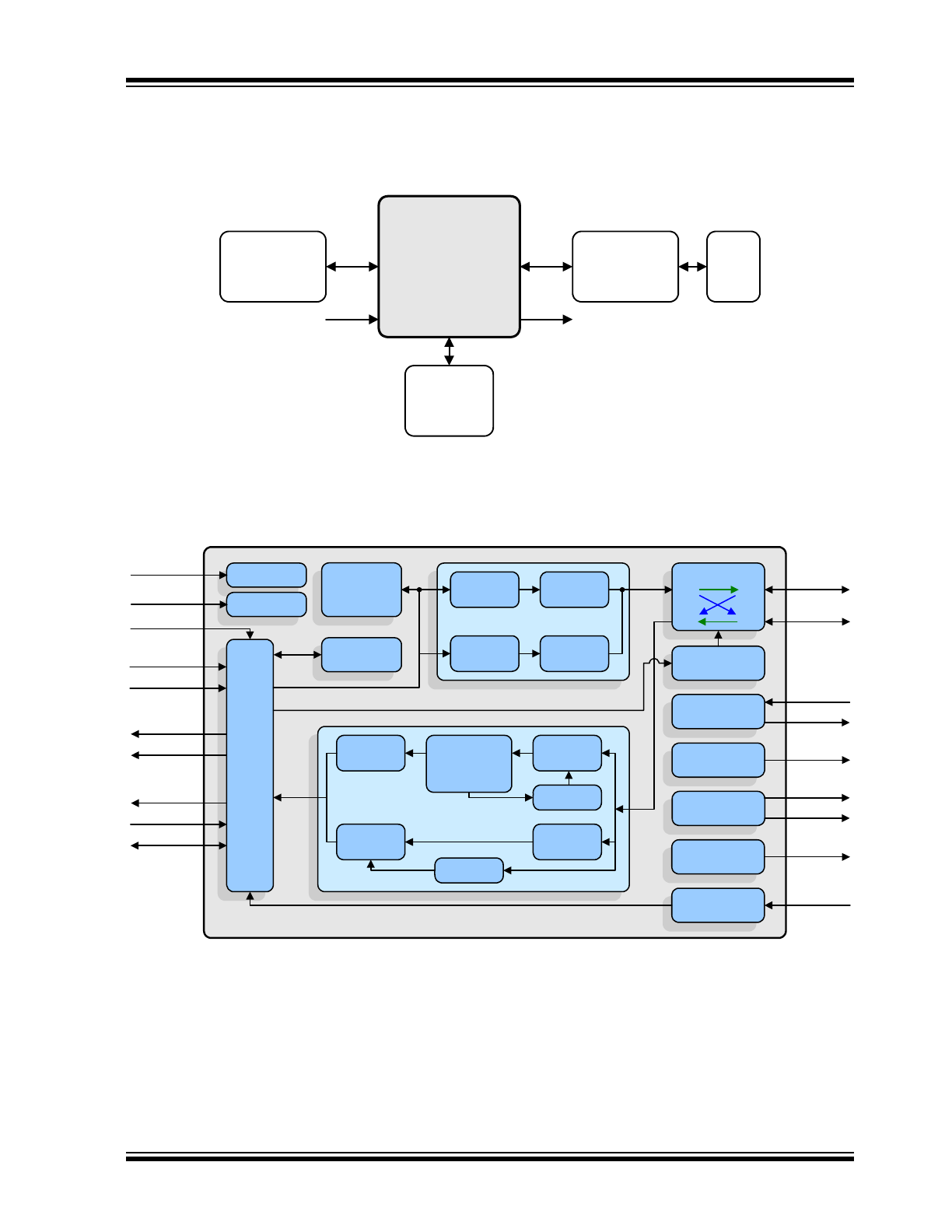
FIGURE 1-1:
SYSTEM BLOCK DIAGRAM
LAN8720A/
LAN8720Ai
10/100
Ethernet
MAC
RMII
Mode
LED
Transformer
Crystal or
Clock
Oscillator
MDI
RJ45
FIGURE 1-2:
ARCHITECTURAL OVERVIEW
R
M
II
Lo
gi
c
Interrupt
Generator
LEDs
PLL
Receiver
DSP System:
Clock
Data Recovery
Equalizer
Squeltch
& Filters
Analog-to-
Digital
10M RX
Logic
100M RX
Logic
100M PLL
10M PLL
Transmitter
10M
Transmitter
100M
Transmitter
10M TX
Logic
100M TX
Logic
Central Bias
PHY Address
Latches
LAN8720A/LAN8720Ai
RBIAS
LED1
nINT
XTAL2
XTAL1/CLKIN
LED2
Management
Control
Mode Control
Reset Control
MDIX
Control
HP Auto-MDIX
RXP/RXN
TXP/TXN
TXD[0:1]
TXEN
RXD[0:1]
RXER
CRS_DV
MDC
MDIO
Auto-
Negotiation
RMIISEL
nRST
MODE[0:2]
SMI
PHYAD0
2016 Microchip Technology Inc.
DS00002165B-page 5
LAN8720A/LAN8720AI
LAN8720A/LAN8720AI
DS00002165B-page 6
2016 Microchip Technology Inc.
2.0
PIN DESCRIPTION AND CONFIGURATION
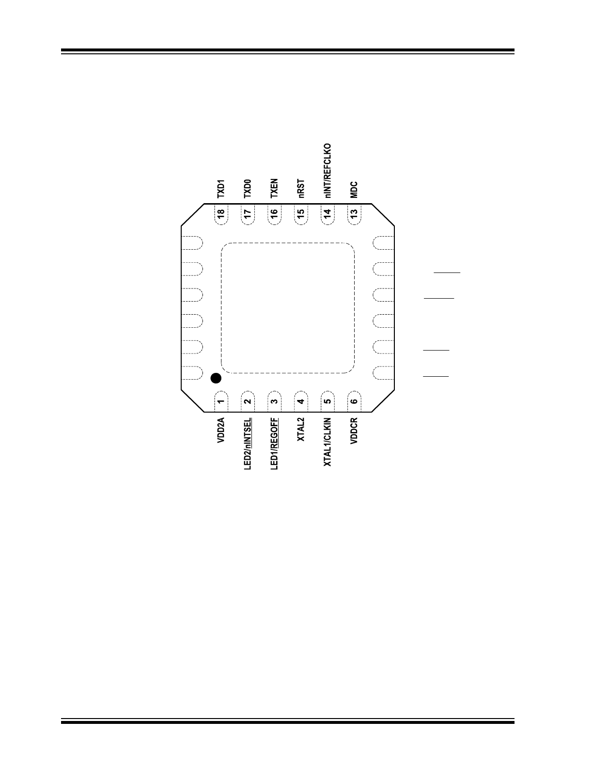
FIGURE 2-1:
24-QFN/SQFN PIN ASSIGNMENTS (TOP VIEW)
VSS
NOTE: Exposed pad (VSS) on bottom of package must be connected to ground
LAN8720A/LAN8720Ai
(TOP VIEW)
MDIO
7
8
9
10
11
12
24
23
22
21
20
19
VDD1A
TXN
TXP
RXN
RXP
RBIAS
CRS_DV/MODE2
RXER/PHYAD0
VDDIO
RXD0/MODE0
RXD1/MODE1
Note 2-1
When a lower case “n” is used at the beginning of the signal name, it indicates that the signal is
active low. For example, nRST indicates that the reset signal is active low.
Note 2-2
The buffer type for each signal is indicated in the BUFFER TYPE column. A description of the buffer
types is provided in
Section 2.2
.

2016 Microchip Technology Inc.
DS00002165B-page 7
LAN8720A/LAN8720AI
TABLE 2-1:
RMII SIGNALS
Num Pins
Name
Symbol
Buffer
Type
Description
1
Transmit
Data 0
TXD0
VIS
The MAC transmits data to the transceiver using
this signal.
1
Transmit
Data 1
TXD1
VIS
The MAC transmits data to the transceiver using
this signal.
1
Transmit
Enable
TXEN
VIS
(PD)
Indicates that valid transmission data is present
on TXD[1:0].
1
Receive
Data 0
RXD0
VO8
Bit 0 of the 2 data bits that are sent by the trans-
ceiver on the receive path.
PHY Operat-
ing Mode 0
Configuration
Strap
MODE0
VIS
(PU)
Combined with MODE1 and MODE2, this config-
uration strap sets the default PHY mode.
See
Note 2-3
for more information on configura-
tion straps.
Note: Refer to
Section 3.7.2, "MODE[2:0]:
Mode Configuration," on page 30
for
additional details.
1
Receive
Data 1
RXD1
VO8
Bit 1 of the 2 data bits that are sent by the trans-
ceiver on the receive path.
PHY Operat-
ing Mode 1
Configuration
Strap
MODE1
VIS
(PU)
Combined with MODE0 and MODE2, this config-
uration strap sets the default PHY mode.
See
Note 2-3
for more information on configura-
tion straps.
Note: Refer to
Section 3.7.2, "MODE[2:0]:
Mode Configuration," on page 30
for
additional details.
1
Receive Error
RXER
VO8
This signal is asserted to indicate that an error
was detected somewhere in the frame presently
being transferred from the transceiver.
PHY Address
0
Configuration
Strap
PHYAD0
VIS
(PD)
This configuration strap sets the transceiver’s SMI
address.
See
Note 2-3
for more information on configura-
tion straps.
Note: Refer to
Section 3.7.1, "PHYAD[0]: PHY
Address Configuration," on page 26
for
additional information.
LAN8720A/LAN8720AI
DS00002165B-page 8
2016 Microchip Technology Inc.
Note 2-3
Configuration strap values are latched on power-on reset and system reset. Configuration straps are
identified by an underlined symbol name. Signals that function as configuration straps must be
augmented with an external resistor when connected to a load. Refer to
Section 3.7, "Configuration
Straps," on page 29
for additional information.
1
Carrier Sense
/ Receive
Data Valid
CRS_DV
VO8
This signal is asserted to indicate the receive
medium is non-idle. When a 10BASE-T packet is
received, CRS_DV is asserted, but RXD[1:0] is
held low until the SFD byte (10101011) is
received.
Note: Per the RMII standard, transmitted data is
not looped back onto the receive data
pins in 10BASE-T half-duplex mode.
PHY Operat-
ing Mode 2
Configuration
Strap
MODE2
VIS
(PU)
Combined with MODE0 and MODE1, this config-
uration strap sets the default PHY mode.
See
Note 2-3
for more information on configura-
tion straps.
Note: Refer to
Section 3.7.2, "MODE[2:0]:
Mode Configuration," on page 27
for
additional details.
TABLE 2-2:
LED PINS
NUM PINS
NAME
SYMBOL
BUFFER
TYPE
DESCRIPTION
1
LED 1
LED1
O12
Link activity LED Indication. This pin is driven
active when a valid link is detected and blinks
when activity is detected.
Note: Refer to
Section 3.8.1, "LEDs," on
page 32
for additional LED information.
Regulator Off
Configuration
Strap
REGOFF
IS
(PD)
This configuration strap is used to disable the
internal 1.2V regulator. When the regulator is dis-
abled, external 1.2V must be supplied to VDDCR.
• When REGOFF is pulled high to VDD2A with
an external resistor, the internal regulator is
disabled.
• When REGOFF is floating or pulled low, the
internal regulator is enabled (default).
See
Note 2-4
for more information on configura-
tion straps.
Note: Refer to
Section 3.7.4, "REGOFF:
Internal +1.2V Regulator Configuration,"
on page 32
for additional details.
TABLE 2-1:
RMII SIGNALS (CONTINUED)
Num Pins
Name
Symbol
Buffer
Type
Description
2016 Microchip Technology Inc.
DS00002165B-page 9
LAN8720A/LAN8720AI
Note 2-4
Configuration strap values are latched on power-on reset and system reset. Configuration straps are
identified by an underlined symbol name. Signals that function as configuration straps must be
augmented with an external resistor when connected to a load. Refer to
Section 3.7, "Configuration
Straps," on page 29
for additional information.
TABLE 2-3:
SERIAL MANAGEMENT INTERFACE (SMI) PINS
Num PINs
NAME
SYMBOL
BUFFER
TYPE
DESCRIPTION
1
SMI Data
Input/Output
MDIO
VIS/
VOD8
Serial Management Interface data input/output
1
SMI Clock
MDC
VIS
Serial Management Interface clock
1
LED 2
LED2
O12
Link Speed LED Indication. This pin is driven
active when the operating speed is 100Mbps. It is
inactive when the operating speed is 10Mbps or
during line isolation.
Note: Refer to
Section 3.8.1, "LEDs," on
page 32
for additional LED information.
nINT/
REFCLKO
Function
Select
Configuration
Strap
nINTSEL
IS
(PU)
This configuration strap selects the mode of the
nINT/REFCLKO pin.
• When nINTSEL is floated or pulled to
VDD2A, nINT is selected for operation on the
nINT/REFCLKO pin (default).
• When nINTSEL is pulled low to VSS, REF-
CLKO is selected for operation on the nINT/
REFCLKO pin.
See
Note 2-4
for more information on configura-
tion straps.
Note: Refer to See
Section 3.8.1.2, "nINTSEL
and LED2 Polarity Selection," on page 33
for additional information.
TABLE 2-4:
ETHERNET PINS
Num PINs
NAME
SYMBOL
BUFFER
TYPE
DESCRIPTION
1
Ethernet TX/
RX Positive
Channel 1
TXP
AIO
Transmit/Receive Positive Channel 1
1
Ethernet TX/
RX Negative
Channel 1
TXN
AIO
Transmit/Receive Negative Channel 1
TABLE 2-2:
LED PINS (CONTINUED)
NUM PINS
NAME
SYMBOL
BUFFER
TYPE
DESCRIPTION

LAN8720A/LAN8720AI
DS00002165B-page 10
2016 Microchip Technology Inc.
1
Ethernet TX/
RX Positive
Channel 2
RXP
AIO
Transmit/Receive Positive Channel 2
1
Ethernet TX/
RX Negative
Channel 2
RXN
AIO
Transmit/Receive Negative Channel 2
TABLE 2-5:
MISCELLANEOUS PINS
Num PINs
NAME
SYMBOL
BUFFER
TYPE
DESCRIPTION
1
External
Crystal
Input
XTAL1
ICLK
External crystal input
External
Clock Input
CLKIN
ICLK
Single-ended clock oscillator input.
Note: When using a single ended clock
oscillator, XTAL2 should be left
unconnected.
1
External
Crystal Out-
put
XTAL2
OCLK
External crystal output
1
External
Reset
nRST
VIS
(PU)
System reset. This signal is active low.
1
Interrupt Out-
put
nINT
VOD8
(PU)
Active low interrupt output. Place an external
resistor pull-up to VDDIO.
Note: Refer to
Section 3.6, "Interrupt
Management," on page 24
for additional
details on device interrupts.
Note: Refer to
Section 3.8.1.2, "nINTSEL and
LED2 Polarity Selection," on page 32
for
details on how the nINTSEL configuration
strap is used to determine the function of
this pin.
Reference
Clock Output
REFCLKO
VO8
This optional 50MHz clock output is derived from
the 25MHz crystal oscillator. REFCLKO is select-
able via the nINTSEL configuration strap.
Note: Refer
Section 3.7.4.2, "REF_CLK Out
Mode," on page 29
for additional details.
Note: Refer to
Section 3.8.1.2, "nINTSEL and
LED2 Polarity Selection," on page 32
for
details on how the nINTSEL configuration
strap is used to determine the function of
this pin.
TABLE 2-4:
ETHERNET PINS (CONTINUED)
Num PINs
NAME
SYMBOL
BUFFER
TYPE
DESCRIPTION
2016 Microchip Technology Inc.
DS00002165B-page 1
Highlights
• Single-Chip Ethernet Physical Layer Transceiver
(PHY)
• Comprehensive flexPWR
®
Technology
- Flexible Power Management Architecture
- LVCMOS Variable I/O voltage range: +1.6V
to +3.6V
- Integrated 1.2V regulator
• HP Auto-MDIX support
• Miniature 24-pin QFN/SQFN lead-free RoHS
compliant packages (4 x 4mm).
Target Applications
• Set-Top Boxes
• Networked Printers and Servers
• Test Instrumentation
• LAN on Motherboard
• Embedded Telecom Applications
• Video Record/Playback Systems
• Cable Modems/Routers
• DSL Modems/Routers
• Digital Video Recorders
• IP and Video Phones
• Wireless Access Points
• Digital Televisions
• Digital Media Adapters/Servers
• Gaming Consoles
• POE Applications (Refer to Application Note
17.18)
Key Benefits
• High-Performance 10/100 Ethernet Transceiver
- Compliant with IEEE802.3/802.3u (Fast
Ethernet)
- Compliant with ISO 802-3/IEEE 802.3
(10BASE-T)
- Loop-back modes
- Auto-negotiation
- Automatic polarity detection and correction
- Link status change wake-up detection
- Vendor specific register functions
- Supports the reduced pin count RMII inter-
face
• Power and I/Os
- Various low power modes
- Integrated power-on reset circuit
- Two status LED outputs
- Latch-Up Performance Exceeds 150mA per
EIA/JESD 78, Class II
- May be used with a single 3.3V supply
• Additional Features
- Ability to use a low cost 25Mhz crystal for
reduced BOM
• Packaging
- 24-pin QFN/SQFN (4x4 mm) Lead-Free
RoHS Compliant package with RMII
• Environmental
- Extended commercial temperature range
(0°C to +85°C)
- Industrial temperature range version avail-
able (-40°C to +85°C)
LAN8720A/LAN8720AI
Small Footprint RMII 10/100 Ethernet
Transceiver with HP Auto-MDIX Support
TO OUR VALUED CUSTOMERS
It is our intention to provide our valued customers with the best documentation possible to ensure successful use of your Microchip
products. To this end, we will continue to improve our publications to better suit your needs. Our publications will be refined and
enhanced as new volumes and updates are introduced.
If you have any questions or comments regarding this publication, please contact the Marketing Communications Department via
E-mail at
docerrors@microchip.com
. We welcome your feedback.
Most Current Data Sheet
To obtain the most up-to-date version of this data sheet, please register at our Worldwide Web site at:
http://www.microchip.com
You can determine the version of a data sheet by examining its literature number found on the bottom outside corner of any page.
The last character of the literature number is the version number, (e.g., DS30000000A is version A of document DS30000000).
Errata
An errata sheet, describing minor operational differences from the data sheet and recommended workarounds, may exist for cur-
rent devices. As device/documentation issues become known to us, we will publish an errata sheet. The errata will specify the
revision of silicon and revision of document to which it applies.
To determine if an errata sheet exists for a particular device, please check with one of the following:
• Microchip’s Worldwide Web site;
http://www.microchip.com
• Your local Microchip sales office (see last page)
When contacting a sales office, please specify which device, revision of silicon and data sheet (include -literature number) you are
using.
Customer Notification System
Register on our web site at
www.microchip.com
to receive the most current information on all of our products.
LAN8720A/LAN8720AI
DS00002165B-page 2
2016 Microchip Technology Inc.
2016 Microchip Technology Inc.
DS00002165B-page 3
LAN8720A/LAN8720AI
Table of Contents
1.0 Introduction ..................................................................................................................................................................................... 4
2.0 Pin Description and Configuration .................................................................................................................................................. 6
3.0 Functional Description .................................................................................................................................................................. 14
4.0 Register Descriptions .................................................................................................................................................................... 41
5.0 Operational Characteristics ........................................................................................................................................................... 52
6.0 Package Information ..................................................................................................................................................................... 66
7.0 Application Notes .......................................................................................................................................................................... 71
Appendix A: Data Sheet Revision History ........................................................................................................................................... 73
The Microchip Web Site ...................................................................................................................................................................... 74
Customer Change Notification Service ............................................................................................................................................... 74
Customer Support ............................................................................................................................................................................... 74
Product Identification System ............................................................................................................................................................. 75
LAN8720A/LAN8720AI
DS00002165B-page 4
2016 Microchip Technology Inc.
1.0
INTRODUCTION
1.1
General Terms and Conventions
The following is list of the general terms used throughout this document:
BYTE
8-bits
FIFO
First In First Out buffer; often used for elasticity buffer
MAC
Media Access Controller
RMII™
Reduced Media Independent Interface
TM
N/A
Not Applicable
X
Indicates that a logic state is “don’t care” or undefined.
RESERVED
Refers to a reserved bit field or address. Unless otherwise
noted, reserved bits must always be zero for write opera-
tions. Unless otherwise noted, values are not guaranteed
when reading reserved bits. Unless otherwise noted, do
not read or write to reserved addresses.
SMI
Serial Management Interface
1.2
General Description
The LAN8720A/LAN8720Ai is a low-power 10BASE-T/100BASE-TX physical layer (PHY) transceiver with variable I/O
voltage that is compliant with the IEEE 802.3-2005 standards.
The LAN8720A/LAN8720Ai supports communication with an Ethernet MAC via a standard RMII interface. It contains a
full-duplex 10-BASE-T/100BASE-TX transceiver and supports 10Mbps (10BASE-T) and 100Mbps (100BASE-TX) oper-
ation. The LAN8720A/LAN8720Ai implements auto-negotiation to automatically determine the best possible speed and
duplex mode of operation. HP Auto-MDIX support allows the use of direct connect or cross-over LAN cables.
The LAN8720A/LAN8720Ai supports both IEEE 802.3-2005 compliant and vendor-specific register functions. However,
no register access is required for operation. The initial configuration may be selected via the configuration pins as
described in
Section 3.7, "Configuration Straps," on page 29
. Register-selectable configuration options may be used to
further define the functionality of the transceiver.
Per IEEE 802.3-2005 standards, all digital interface pins are tolerant to 3.6V. The device can be configured to operate
on a single 3.3V supply utilizing an integrated 3.3V to 1.2V linear regulator. The linear regulator may be optionally dis-
abled, allowing usage of a high efficiency external regulator for lower system power dissipation.
The LAN8720A/LAN8720Ai is available in both extended commercial and industrial temperature range versions. A typ-
ical system application is shown in
Figure 1-1
.
FIGURE 1-1:
SYSTEM BLOCK DIAGRAM
LAN8720A/
LAN8720Ai
10/100
Ethernet
MAC
RMII
Mode
LED
Transformer
Crystal or
Clock
Oscillator
MDI
RJ45
FIGURE 1-2:
ARCHITECTURAL OVERVIEW
R
M
II
Lo
gi
c
Interrupt
Generator
LEDs
PLL
Receiver
DSP System:
Clock
Data Recovery
Equalizer
Squeltch
& Filters
Analog-to-
Digital
10M RX
Logic
100M RX
Logic
100M PLL
10M PLL
Transmitter
10M
Transmitter
100M
Transmitter
10M TX
Logic
100M TX
Logic
Central Bias
PHY Address
Latches
LAN8720A/LAN8720Ai
RBIAS
LED1
nINT
XTAL2
XTAL1/CLKIN
LED2
Management
Control
Mode Control
Reset Control
MDIX
Control
HP Auto-MDIX
RXP/RXN
TXP/TXN
TXD[0:1]
TXEN
RXD[0:1]
RXER
CRS_DV
MDC
MDIO
Auto-
Negotiation
RMIISEL
nRST
MODE[0:2]
SMI
PHYAD0
2016 Microchip Technology Inc.
DS00002165B-page 5
LAN8720A/LAN8720AI
LAN8720A/LAN8720AI
DS00002165B-page 6
2016 Microchip Technology Inc.
2.0
PIN DESCRIPTION AND CONFIGURATION
FIGURE 2-1:
24-QFN/SQFN PIN ASSIGNMENTS (TOP VIEW)
VSS
NOTE: Exposed pad (VSS) on bottom of package must be connected to ground
LAN8720A/LAN8720Ai
(TOP VIEW)
MDIO
7
8
9
10
11
12
24
23
22
21
20
19
VDD1A
TXN
TXP
RXN
RXP
RBIAS
CRS_DV/MODE2
RXER/PHYAD0
VDDIO
RXD0/MODE0
RXD1/MODE1
Note 2-1
When a lower case “n” is used at the beginning of the signal name, it indicates that the signal is
active low. For example, nRST indicates that the reset signal is active low.
Note 2-2
The buffer type for each signal is indicated in the BUFFER TYPE column. A description of the buffer
types is provided in
Section 2.2
.
2016 Microchip Technology Inc.
DS00002165B-page 7
LAN8720A/LAN8720AI
TABLE 2-1:
RMII SIGNALS
Num Pins
Name
Symbol
Buffer
Type
Description
1
Transmit
Data 0
TXD0
VIS
The MAC transmits data to the transceiver using
this signal.
1
Transmit
Data 1
TXD1
VIS
The MAC transmits data to the transceiver using
this signal.
1
Transmit
Enable
TXEN
VIS
(PD)
Indicates that valid transmission data is present
on TXD[1:0].
1
Receive
Data 0
RXD0
VO8
Bit 0 of the 2 data bits that are sent by the trans-
ceiver on the receive path.
PHY Operat-
ing Mode 0
Configuration
Strap
MODE0
VIS
(PU)
Combined with MODE1 and MODE2, this config-
uration strap sets the default PHY mode.
See
Note 2-3
for more information on configura-
tion straps.
Note: Refer to
Section 3.7.2, "MODE[2:0]:
Mode Configuration," on page 30
for
additional details.
1
Receive
Data 1
RXD1
VO8
Bit 1 of the 2 data bits that are sent by the trans-
ceiver on the receive path.
PHY Operat-
ing Mode 1
Configuration
Strap
MODE1
VIS
(PU)
Combined with MODE0 and MODE2, this config-
uration strap sets the default PHY mode.
See
Note 2-3
for more information on configura-
tion straps.
Note: Refer to
Section 3.7.2, "MODE[2:0]:
Mode Configuration," on page 30
for
additional details.
1
Receive Error
RXER
VO8
This signal is asserted to indicate that an error
was detected somewhere in the frame presently
being transferred from the transceiver.
PHY Address
0
Configuration
Strap
PHYAD0
VIS
(PD)
This configuration strap sets the transceiver’s SMI
address.
See
Note 2-3
for more information on configura-
tion straps.
Note: Refer to
Section 3.7.1, "PHYAD[0]: PHY
Address Configuration," on page 26
for
additional information.
LAN8720A/LAN8720AI
DS00002165B-page 8
2016 Microchip Technology Inc.
Note 2-3
Configuration strap values are latched on power-on reset and system reset. Configuration straps are
identified by an underlined symbol name. Signals that function as configuration straps must be
augmented with an external resistor when connected to a load. Refer to
Section 3.7, "Configuration
Straps," on page 29
for additional information.
1
Carrier Sense
/ Receive
Data Valid
CRS_DV
VO8
This signal is asserted to indicate the receive
medium is non-idle. When a 10BASE-T packet is
received, CRS_DV is asserted, but RXD[1:0] is
held low until the SFD byte (10101011) is
received.
Note: Per the RMII standard, transmitted data is
not looped back onto the receive data
pins in 10BASE-T half-duplex mode.
PHY Operat-
ing Mode 2
Configuration
Strap
MODE2
VIS
(PU)
Combined with MODE0 and MODE1, this config-
uration strap sets the default PHY mode.
See
Note 2-3
for more information on configura-
tion straps.
Note: Refer to
Section 3.7.2, "MODE[2:0]:
Mode Configuration," on page 27
for
additional details.
TABLE 2-2:
LED PINS
NUM PINS
NAME
SYMBOL
BUFFER
TYPE
DESCRIPTION
1
LED 1
LED1
O12
Link activity LED Indication. This pin is driven
active when a valid link is detected and blinks
when activity is detected.
Note: Refer to
Section 3.8.1, "LEDs," on
page 32
for additional LED information.
Regulator Off
Configuration
Strap
REGOFF
IS
(PD)
This configuration strap is used to disable the
internal 1.2V regulator. When the regulator is dis-
abled, external 1.2V must be supplied to VDDCR.
• When REGOFF is pulled high to VDD2A with
an external resistor, the internal regulator is
disabled.
• When REGOFF is floating or pulled low, the
internal regulator is enabled (default).
See
Note 2-4
for more information on configura-
tion straps.
Note: Refer to
Section 3.7.4, "REGOFF:
Internal +1.2V Regulator Configuration,"
on page 32
for additional details.
TABLE 2-1:
RMII SIGNALS (CONTINUED)
Num Pins
Name
Symbol
Buffer
Type
Description
2016 Microchip Technology Inc.
DS00002165B-page 9
LAN8720A/LAN8720AI
Note 2-4
Configuration strap values are latched on power-on reset and system reset. Configuration straps are
identified by an underlined symbol name. Signals that function as configuration straps must be
augmented with an external resistor when connected to a load. Refer to
Section 3.7, "Configuration
Straps," on page 29
for additional information.
TABLE 2-3:
SERIAL MANAGEMENT INTERFACE (SMI) PINS
Num PINs
NAME
SYMBOL
BUFFER
TYPE
DESCRIPTION
1
SMI Data
Input/Output
MDIO
VIS/
VOD8
Serial Management Interface data input/output
1
SMI Clock
MDC
VIS
Serial Management Interface clock
1
LED 2
LED2
O12
Link Speed LED Indication. This pin is driven
active when the operating speed is 100Mbps. It is
inactive when the operating speed is 10Mbps or
during line isolation.
Note: Refer to
Section 3.8.1, "LEDs," on
page 32
for additional LED information.
nINT/
REFCLKO
Function
Select
Configuration
Strap
nINTSEL
IS
(PU)
This configuration strap selects the mode of the
nINT/REFCLKO pin.
• When nINTSEL is floated or pulled to
VDD2A, nINT is selected for operation on the
nINT/REFCLKO pin (default).
• When nINTSEL is pulled low to VSS, REF-
CLKO is selected for operation on the nINT/
REFCLKO pin.
See
Note 2-4
for more information on configura-
tion straps.
Note: Refer to See
Section 3.8.1.2, "nINTSEL
and LED2 Polarity Selection," on page 33
for additional information.
TABLE 2-4:
ETHERNET PINS
Num PINs
NAME
SYMBOL
BUFFER
TYPE
DESCRIPTION
1
Ethernet TX/
RX Positive
Channel 1
TXP
AIO
Transmit/Receive Positive Channel 1
1
Ethernet TX/
RX Negative
Channel 1
TXN
AIO
Transmit/Receive Negative Channel 1
TABLE 2-2:
LED PINS (CONTINUED)
NUM PINS
NAME
SYMBOL
BUFFER
TYPE
DESCRIPTION
LAN8720A/LAN8720AI
DS00002165B-page 10
2016 Microchip Technology Inc.
1
Ethernet TX/
RX Positive
Channel 2
RXP
AIO
Transmit/Receive Positive Channel 2
1
Ethernet TX/
RX Negative
Channel 2
RXN
AIO
Transmit/Receive Negative Channel 2
TABLE 2-5:
MISCELLANEOUS PINS
Num PINs
NAME
SYMBOL
BUFFER
TYPE
DESCRIPTION
1
External
Crystal
Input
XTAL1
ICLK
External crystal input
External
Clock Input
CLKIN
ICLK
Single-ended clock oscillator input.
Note: When using a single ended clock
oscillator, XTAL2 should be left
unconnected.
1
External
Crystal Out-
put
XTAL2
OCLK
External crystal output
1
External
Reset
nRST
VIS
(PU)
System reset. This signal is active low.
1
Interrupt Out-
put
nINT
VOD8
(PU)
Active low interrupt output. Place an external
resistor pull-up to VDDIO.
Note: Refer to
Section 3.6, "Interrupt
Management," on page 24
for additional
details on device interrupts.
Note: Refer to
Section 3.8.1.2, "nINTSEL and
LED2 Polarity Selection," on page 32
for
details on how the nINTSEL configuration
strap is used to determine the function of
this pin.
Reference
Clock Output
REFCLKO
VO8
This optional 50MHz clock output is derived from
the 25MHz crystal oscillator. REFCLKO is select-
able via the nINTSEL configuration strap.
Note: Refer
Section 3.7.4.2, "REF_CLK Out
Mode," on page 29
for additional details.
Note: Refer to
Section 3.8.1.2, "nINTSEL and
LED2 Polarity Selection," on page 32
for
details on how the nINTSEL configuration
strap is used to determine the function of
this pin.
TABLE 2-4:
ETHERNET PINS (CONTINUED)
Num PINs
NAME
SYMBOL
BUFFER
TYPE
DESCRIPTION