

2016-2017 Microchip Technology Inc.
DS00002112B-page 1
Target Applications
• Industrial Ethernet Applications that Employ IEEE
802.3-Compliant MACs. (Ethernet/IP, Profinet,
MODBUS TCP, etc.)
• VoIP Phone
• Set-Top/Game Box
• Automotive
• Industrial Control
• IPTV POF
• SOHO Residential Gateway with Full-Wire Speed
of Four LAN Ports
• Broadband Gateway/Firewall/VPN
• Integrated DSL/Cable Modem
• Wireless LAN Access Point + Gateway
• Standalone 10/100 Switch
• Networked Measurement and Control Systems
Features
• Management Capabilities
- The KSZ8795CLX Includes All the Functions
of a 10/100BASE-T/TX Switch System Which
Combines a Switch Engine, Frame Buffer
Management, Address Look-Up Table,
Queue Management, MIB Counters, Media
Access Controllers (MAC), and PHY Trans-
ceivers
- Non-Blocking Store-and-Forward Switch
Fabric Assures Fast Packet Delivery by Uti-
lizing a 1024-Entries Forwarding Table
- Port Mirroring/Monitoring/Sniffing: Ingress
and/or Egress Traffic to Any Port
- MIB Counters for Fully-Compliant Statistics
Gathering (36 Counters per Port)
- Support Hardware for Port-Based Flush and
Freeze Command in MIB Counter.
- Multiple Loopback of Remote, PHY, and MAC
Modes Support for the Diagnostics
- Rapid Spanning Tree Support (RSTP) for
Topology Management and Ring/Linear
Recovery
• Robust PHY Ports
- Four Integrated IEEE 802.3/802.3u-Compli-
ant Ethernet Transceivers Supporting
10BASE-T and 100BASE-TX
-
- 802.1az EEE Supported
- On-Chip Termination Resistors and Internal
Biasing for Differential Pairs to Reduce
Power
- HP Auto MDI/MDI-X Crossover Support Elim-
inates the Need to Differentiate Between
Straight or Crossover Cables in Applications
• MAC and GMAC Ports
- Four Internal Media Access Control (MAC1 to
MAC4) Units and One Internal Gigabit Media
Access Control (GMAC5) Unit
- GMII, RGMII, MII or RMII Interfaces Support
for the Port 5 GMAC5 with Uplink
- 2 KByte Jumbo Packet Support
- Tail Tagging Mode (One Byte Added Before
FCS) Support on Port 5 to Inform the Proces-
sor in which the Ingress Port Receives the
Packet and its Priority
- Supports Reduced Media Independent Inter-
face (RMII) with 50 MHz Reference Clock
Output
- Supports Media Independent Interface (MII)
in Either PHY Mode or MAC Mode on Port 5
- LinkMD
®
Cable Diagnostic Capabilities for
Determining Cable Opens, Shorts, and
Length
• Advanced Switch Capabilities
- Non-Blocking Store-and-Forward Switch
Fabric Assures Fast Packet Delivery by Uti-
lizing 1024 Entry Forwarding Table
- 64 KB Frame Buffer RAM
- IEEE 802.1q VLAN Support for up to 128
Active VLAN Groups (Full-Range 4096 of
VLAN IDs)
- IEEE 802.1p/Q Tag Insertion or Removal on
a Per Port Basis (Egress)
- VLAN ID Tag/Untag Options on Per Port
Basis
- Fully Compliant with IEEE 802.3/802.3u
Standards
- IEEE 802.3x Full-Duplex with Force-Mode
Option and Half-Duplex Back-Pressure Colli-
sion Flow Control
- IEEE 802.1w Rapid Spanning Tree Protocol
Support
KSZ8795CLX
Integrated 5-Port 10/100-Managed Ethernet
Switch with Gigabit GMII/RGMII and MII/
RMII Interfaces

KSZ8795CLX
2016-2017 Microchip Technology Inc.
DS00002112B-page 2
- IGMP v1/v2/v3 Snooping for Multicast Packet
Filtering
- QoS/CoS Packets Prioritization Support:
802.1p, DiffServ-Based and Re-Mapping of
802.1p Priority Field Per Port Basis on Four
Priority Levels
- IPv4/IPv6 QoS Support
- IPV6 Multicast Listener Discovery (MLD)
Snooping
- Programmable Rate Limiting at the Ingress
and Egress Ports on a Per Port Basis
- Jitter-Free Per Packet Based Rate Limiting
Support
- Tail Tag Mode (1 byte Added before FCS)
Support on Port 5 to Inform the Processor
which Ingress Port Receives the Packet
- Broadcast Storm Protection with Percentage
Control (Global and Per Port Basis)
- 1K Entry Forwarding Table with 64 KB Frame
Buffer
- 4 Priority Queues with Dynamic Packet Map-
ping for IEEE 802.1P, IPV4 TOS (DIFF-
SERV), IPv6 Traffic Class, etc.
- Supports WoL Using AMD’s Magic Packet
- VLAN and Address Filtering
- Supports 802.1x Port-Based Security,
Authentication and MAC-Based Authentica-
tion via Access Control Lists (ACL)
- Provides Port-Based and Rule-Based ACLs
to Support Layer 2 MAC SA/DA Address,
Layer 3 IP Address and IP Mask, Layer 4
TCP/UDP Port Number, IP Protocol, TCP
Flag and Compensation for the Port Security
Filtering
- Ingress and Egress Rate Limit Based on Bit
per Second (bps) and Packet-Based Rate
Limiting (pps)
• Configuration Registers Access
- High-Speed SPI (4-Wire, up to 50 MHz) Inter-
face to Access All Internal Registers
- MII Management (MIIM, MDC/MDIO 2-Wire)
Interface to Access All PHY Registers per
Clause 22.2.4.5 of the IEEE 802.3 Specifica-
tion
- I/O Pin Strapping Facility to Set Certain Reg-
ister Bits from I/O Pins During Reset Time
- Control Registers Configurable On-the-Fly
• Power and Power Management
- Full-Chip Software Power-Down (All Register
Values are Not Saved and Strap-In value Will
Re-Strap after it Releases the Power-Down)
- Per-Port Software Power-Down
- Energy Detect Power-Down (EDPD), which
Disables the PHY Transceiver When Cables
are Removed
- Supports IEEE P802.3az Energy Efficient
Ethernet (EEE) to Reduce Power Consump-
tion in Transceivers in LPI State Even
Though Cables are Not Removed
- Dynamic Clock Tree Control to Reduce
Clocking in Areas that are Not in Use
- Low Power Consumption without Extra
Power Consumption on Transformers
- Voltages: Using External LDO Power Sup-
plies
- Analog V
DDAT
3.3V or 2.5V
- V
DDIO
Support 3.3V, 2.5V, and 1.8V
- Low 1.2V Voltage for Analog and Digital Core
Power
- WoL Support with Configurable Packet Con-
trol
• Additional Features
- Single 25 MHz +50 ppm Reference Clock
Requirement
- Comprehensive Programmable Two-LED
Indicator Support for Link, Activity, Full-/Half-
Duplex, and 10/100 Speed
• Packaging and Environmental
- Commercial Temperature Range: 0°C to
+70°C
- Industrial Temperature Range: –40°C to
+85°C
- Package Available in an 80-Pin LQFP, Lead-
Free (RoHS-Compliant) Package
- Supports Human Body Model (HBM) ESD
Rating of 5 kV
- 0.065 µm CMOS Technology for Lower
Power Consumption

2016-2017 Microchip Technology Inc.
DS00002112B-page 3
KSZ8795CLX
TO OUR VALUED CUSTOMERS
It is our intention to provide our valued customers with the best documentation possible to ensure successful use of your Microchip
products. To this end, we will continue to improve our publications to better suit your needs. Our publications will be refined and
enhanced as new volumes and updates are introduced.
If you have any questions or comments regarding this publication, please contact the Marketing Communications Department via
E-mail at
docerrors@microchip.com
. We welcome your feedback.
Most Current Data Sheet
To obtain the most up-to-date version of this data sheet, please register at our Worldwide Web site at:
http://www.microchip.com
You can determine the version of a data sheet by examining its literature number found on the bottom outside corner of any page.
The last character of the literature number is the version number, (e.g., DS30000000A is version A of document DS30000000).
Errata
An errata sheet, describing minor operational differences from the data sheet and recommended workarounds, may exist for cur-
rent devices. As device/documentation issues become known to us, we will publish an errata sheet. The errata will specify the
revision of silicon and revision of document to which it applies.
To determine if an errata sheet exists for a particular device, please check with one of the following:
• Microchip’s Worldwide Web site;
http://www.microchip.com
• Your local Microchip sales office (see last page)
When contacting a sales office, please specify which device, revision of silicon and data sheet (include -literature number) you are
using.
Customer Notification System
Register on our web site at
www.microchip.com
to receive the most current information on all of our products.

KSZ8795CLX
DS00002112B-page 4
2016-2017 Microchip Technology Inc.
Table of Contents
1.0 Introduction ..................................................................................................................................................................................... 5
2.0 Pin Description and Configuration ................................................................................................................................................... 6
3.0 Functional Description ................................................................................................................................................................... 14
4.0 Device Registers ........................................................................................................................................................................... 47
5.0 Operational Characteristics ......................................................................................................................................................... 113
6.0 Electrical Characteristics ............................................................................................................................................................. 114
7.0 Timing Diagrams ......................................................................................................................................................................... 116
8.0 Reset Circuit ................................................................................................................................................................................ 126
9.0 Selection of Isolation Transformer .............................................................................................................................................. 127
10.0 Selection of Reference Crystal .................................................................................................................................................. 127
11.0 Package Outlines ...................................................................................................................................................................... 128
Appendix A: Data Sheet Revision History ......................................................................................................................................... 129
The Microchip Web Site .................................................................................................................................................................... 130
Customer Change Notification Service ............................................................................................................................................. 130
Customer Support ............................................................................................................................................................................. 130
Product Identification System ............................................................................................................................................................ 131
2016-2017 Microchip Technology Inc.
DS00002112B-page 5
KSZ8795CLX
1.0
INTRODUCTION
1.1
General Description
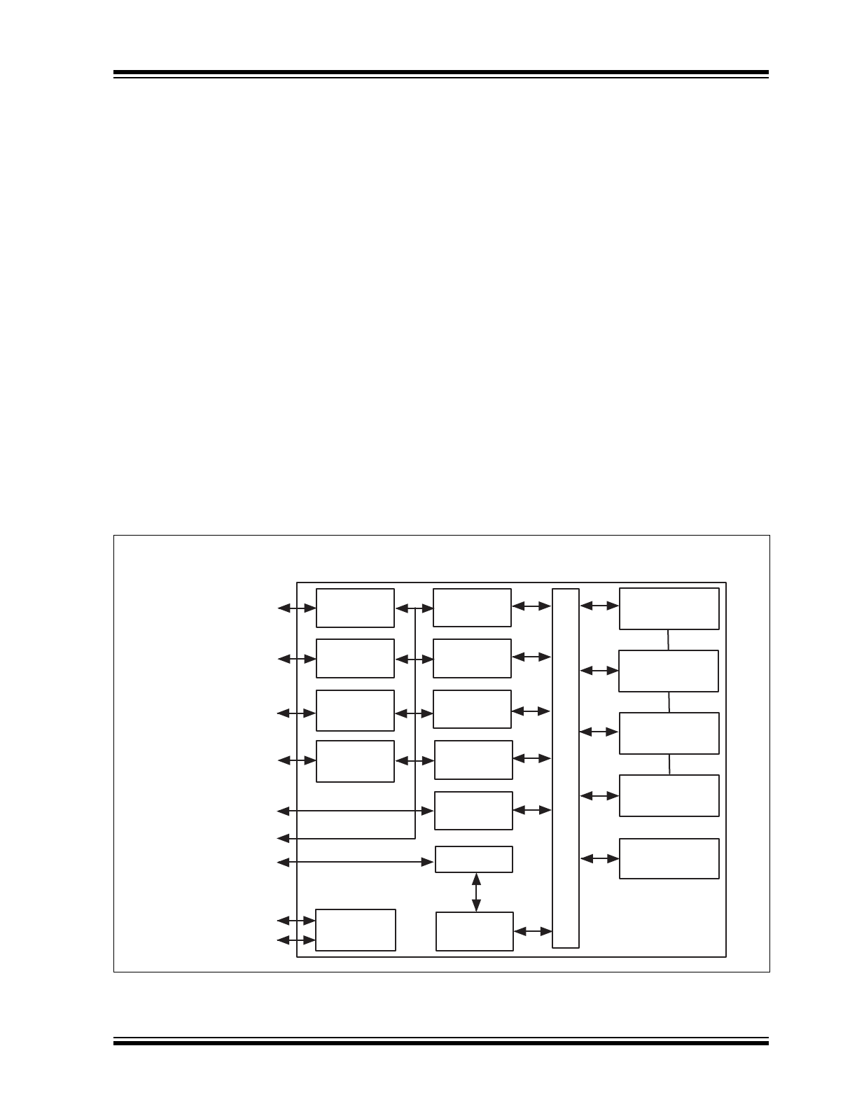
The KSZ8795CLX is a highly integrated, Layer 2-managed, 5-port switch with numerous features designed to reduce
system cost. It is intended for cost-sensitive applications requiring four 10/100 Mbps copper ports and one 10/100/
1000 Mbps Gigabit uplink port. The KSZ8795CLX incorporates a small package outline, lowest power consumption with
internal biasing, and on-chip termination. Its extensive features set includes enhanced power management, program-
mable rate limiting and priority ratio, tagged and port-based VLAN, port-based security and ACL rule-based packet fil-
tering technology, quality-of-service (QoS) priority with four queues, management interfaces, enhanced MIB counters,
high-performance memory bandwidth, and a shared memory-based switch fabric with non-blocking support. The
KSZ8795CLX provides support for multiple CPU data interfaces to effectively address both current and emerging fast
Ethernet and Gigabit Ethernet applications where the port 5 GMAC can be configured to any of GMII, RGMII, MII and
RMII modes.
The KSZ8795CLX is built upon industry-leading Ethernet analog and digital technology, with features designed to off-
load host processing and streamline the overall design.
• Four integrated 10/100BASE-T/TX MAC/PHYs
• One integrated 10/100/1000BASE-T/TX GMAC with selectable GMII, RGMII, MII, and RMII interfaces
• Small 80-pin LQFP package
A robust assortment of power-management features including Energy Efficient Ethernet (EEE), PME, and Wake-on-
LAN (WoL) have been designed-in to satisfy energy-efficient environments.
KSZ8795CLX supports two management interface modes of SPI and MIIM only, SPI access all registers, MIIM mode
access all PHYs registers through MDC/MDIO interface.
FIGURE 1-1:
FUNCTIONAL BLOCK DIAGRAM
AUTO MDI/MDIX
AUTO MDI/MDIX
AUTO MDI/MDIX
AUTO MDI/MDIX
SW5-GMII/RGMII/MII/RMII
MDC, MDI/O FOR MIIM
CONTROL REG SPI I/F
LED0 [4:1]
LED1 [4:1]
KSZ8795
10/100
T/TX
EEE PHY1
10/100
T/TX
EEE PHY2
10/100
T/TX
EEE PHY3
10/100
T/TX
EEE PHY4
LED I/F
10/100
MAC 1
10/100
MAC 2
10/100
MAC 3
10/100
MAC 4
10/100/1000
GMAC 5
SPI
CONTROL
REGISTERS
1K LOOK-UP
ENGINE
QUEUE
MANAGEMENT
BUFFER
MANAGEMENT
FRAME
BUFFER
MIB
COUNTERS
FIFO, FLOW CONTROL, VLAN
T
A
GGING, PRIORITY
KSZ8795CLX
DS00002112B-page 6
2016-2017 Microchip Technology Inc.
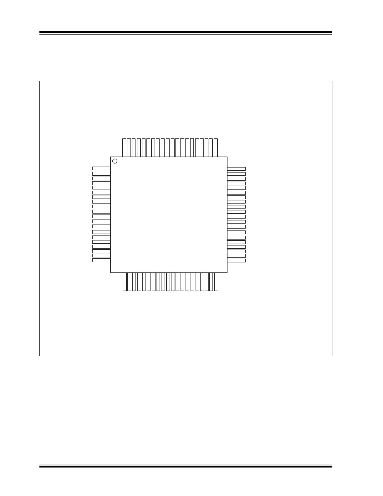
2.0
PIN DESCRIPTION AND CONFIGURATION
FIGURE 2-1:
80-LQFP PIN ASSIGNMENT (TOP VIEW)
XO
XI
GNDA
ISET
VDDA
T33
AT
S
T
NC
VDD12D
RST_N
GNDD
VDDIO
SPIS_N
SDA_MDIO
SCL_MDC
SPIQ
LED1_0
LED1_1
LED2_0
LED2_1
GNDD
GNDA
NC
INTR_N
LED3_1
LED3_0
VDD12D
GNDD
LED4_1
TXEN5/TXDS5_CTL
TXD5_0
LED4_0
TXD5_1
GNDD
VDDIO
TXD5_2
TXD5_3
TXER5
TXD5_4
TXD5_5
TXD5_6
60
59
58
57
56
55
54
53
52
51
50
49
48
47
46
45
44
43
42
41
RXD5_7
RXD5_6
RXD5_5
RXD5_4
PME
REFCLKO
COL5
CRS5
RXER5
RXDV5/CRSDV5/RXD5_CTL
RXD5_3
RXD5_2
VDDIO
GNDD
RXD5_1
RXD5_0
RXC5/GRXC5
TXC5/REFCLKI5/GTXC5
VDD12D
TXD5_7
61
62
63
64
65
66
67
68
69
70
71
72
73
74
75
76
77
78
79
80
21
22
23
24
25
26
27
28
29
30
31
32
33
34
35
36
37
38
39
40
1
2
3
4
5
6
7
8
9
10
11
12
13
14
15
16
17
18
19
20
VDD12A
VDDAT33
GNDA
RXP1
RXM1
TXP1
TXM1
RXP2
RXM2
TXP2
TXM2
VDDAT33
RXP3
RXM3
TXP3
TXM3
RXP4
RXM4
TXP4
TXM4
KSZ8795
(TOP VIEW)

2016-2017 Microchip Technology Inc.
DS00002112B-page 7
KSZ8795CLX
TABLE 2-1:
SIGNALS - KSZ8795CLX
Pin
Number
Pin
Name
Type
Note 2-1
Port
Description
1
VDD12A
P
—
1.2V Core Power
2
VDDAT
P
—
3.3V or 2.5V Analog Power.
3
GNDA
GND
—
Analog Ground.
4
RXP1
I
1
Port 1 Physical Receive Signal + (Differential).
5
RXM1
I
1
Port 1 Physical Receive Signal - (Differential).
6
TXP1
O
1
Port 1 Physical Transmit Signal + (Differential).
7
TXM1
O
1
Port 1 Physical Transmit Signal - (Differential).
8
RXP2
I
2
Port 2 Physical Receive Signal + (Differential).
9
RXM2
I
2
Port 2 Physical Receive Signal - (Differential).
10
TXP2
O
2
Port 2 Physical Transmit Signal + (Differential).
11
TXM2
O
2
Port 2 Physical Transmit Signal - (Differential).
12
VDDAT
P
3.3V or 2.5V Analog Power.
13
RXP3
I
3
Port 3 Physical Receive Signal + (Differential).
14
RXM3
I
3
Port 3 Physical Receive Signal - (Differential).
15
TXP3
O
3
Port 3 Physical Transmit Signal + (Differential).
16
TXM3
O
3
Port 3 Physical Transmit Signal – (Differential).
17
RXP4
I
4
Port 4 Physical Receive Signal + (Differential).
18
RXM4
I
4
Port 4 Physical Receive Signal - (Differential).
19
TXP4
O
4
Port 4 Physical Transmit Signal + (Differential).
20
TXM4
O
4
Port 4 Physical Transmit Signal - (Differential).
21
GNDA
GND
—
Analog Ground.
22
NC
NC
—
No Connect.
23
INTR_N
Opu
—
Interrupt: Active-Low. This pin is open-drain output pin.
Note:
An external pull-up resistor is needed on this pin
when it is in use.
24
LED3_1
Ipu/O
3
Port 3 LED Indicator 1:
See Global Register 11 bits [5:4] for details.
Strap Option: Switch Port 5 GMAC5 interface mode select by
LED3[1:0]
00 = MII for SW5-MII
01 = RMII for SW5-RMII
10 = GMII for SW5-GMII
11 = RGMII for SW5-RGMII (Default)
25
LED3_0
Ipu/O
3
Port 3 LED Indicator 0:
See Global Register 11 bits [5:4] for details.
Strap Option: See LED3_1.

KSZ8795CLX
DS00002112B-page 8
2016-2017 Microchip Technology Inc.
26
VDD12D
P
—
1.2V Core Power.
27
GNDD
GND
—
Digital Ground.
28
LED4_1
Ipu/O
4
Port 4 LED Indicator 1:
See Global Register 11 bits [5:4] for details.
29
TXEN5/
TXD5_CTL
Ipd
5
GMII/MII/RMII: Port 5 Switch transmit enable.
RGMII: Transmit data control.
30
TXD5_0
Ipd
5
GMII/RGMII/MII/RMII: Port 5 switch transmit Bit[0].
31
LED4_0
Ipu/O
4
Port 4 LED Indicator 0:
See Global Register 11 bits [5:4] for details.
32
TXD5_1
Ipd
5
GMII/RGMII/MII/RMII: Port 5 switch transmit Bit[1].
33
GNDD
GND
—
Digital Ground.
34
VDDIO
P
—
3.3V, 2.5V, or 1.8V digital VDD for digital I/O circuitry.
35
TXD5_2
Ipd
5
GMII/RGMII/MII: Port 5 switch transmit Bit[2].
RMII: No connection.
36
TXD5_3
Ipd
5
GMII/RGMII/MII: Port 5 switch transmit Bit[3].
RMII: No connection.
37
TXER5
Ipd
5
GMII/MII: Port 5 switch transmit error.
RGMII/RMII: No connection.
38
TXD5_4
Ipd
5
GMII: Port 5 switch transmit Bit[4].
RGMII/MII/RMII: No connection.
39
TXD5_5
Ipd
5
GMII: Port 5 switch transmit Bit[5].
RGMII/MII/RMII: No connection.
40
TXD5_6
Ipd
5
GMII: Port 5 switch transmit Bit[6].
RGMII/MII/RMII: No connection.
41
TXD5_7
Ipd
5
GMII: Port 5 Switch transmit Bit[7].
RGMII/MII/RMII: No connection.
42
VDD12D
P
—
1.2V Core Power.
43
TXC5/
REFCLKI/
GTXC5
I/O
5
Port 5 Switch GMAC5 Clock Pin:
MII: 2.5/25 MHz clock, PHY mode is output, MAC mode is input.
RMII: Input for receiving 50 MHz clock in normal mode
GMII: Input 125 MHz clock for the transmit
RGMII: Input 125 MHz clock with falling and rising edge to latch
data for the transmit.
44
RXC5/
GRXC5
I/O
5
Port 5 Switch GMAC5 Clock Pin:
MII: 2.5/25 MHz clock, PHY mode is output, MAC mode is input.
RMII: Output 50 MHz reference clock for the receiving/transmit
in the clock mode.
GMII: Output 125 MHz clock for the receiving.
RGMII: Output 125 MHz clock with falling and rising edge to
latch data for the receiving.
TABLE 2-1:
SIGNALS - KSZ8795CLX (CONTINUED)
Pin
Number
Pin
Name
Type
Note 2-1
Port
Description

2016-2017 Microchip Technology Inc.
DS00002112B-page 9
KSZ8795CLX
45
RXD5_0
Ipd/O
5
GMII/RGMII/MII/RMII: Port 5 Switch receive Bit[0].
46
RXD5_1
Ipd/O
5
GMII/RGMII/MII/RMII: Port 5 Switch receive Bit[1].
47
GNDD
GND
—
Digital Ground.
48
VDDIO
P
—
3.3V, 2.5V, or 1.8V digital VDD for digital I/O circuitry.
49
RXD5_2
Ipd/O
5
GMII/RGMII/MII: Port 5 Switch receive Bit[2].
RMII: No connection
50
RXD5_3
Ipd/O
5
GMII/RGMII/MII: Port 5 Switch receive Bit[3].
RMII: No connection
51
RXDV5/
CRSDV5/
RXD5_CTL
Ipd/O
5
GMII/MII: RXDV5 is for Port 5 switch GMII/MII receive data
valid.
RMII: CRSDV5 is for Port 5 RMII carrier sense/receive data
valid output.
RGMII: RXD5_CTL is for Port 5 RGMII receive data control
52
RXER5
Ipd/O
5
GMII/MII: Port 5 Switch receive error.
RGMII/RMII: No connection.
53
CRS5
Ipd/O
5
GMII/MII: Port 5 Switch MII modes carrier sense.
RGMII/RMII: No connection.
54
COL5
Ipd/O
5
GMII/MII: Port 5 Switch MII collision detect.
RGMII/RMII: No connection.
55
REFCLKO
Ipu/O
—
25 MHz Clock Output (Option)
Controlled by the strap pin LED2_0 and the Global Register 11
Bit[1]. Default is enabled; it is better to disable it if it’s not being
used.
56
PME_N
I/O
—
Power Management Event
This output signal indicates that a WoL event has been detected
as a result of a wake-up frame being detected. The KSZ8795-
CLX is requesting the system to wake up from low power mode.
Its assertion polarity is programmable with the default polarity to
be active-low.
57
RXD5_4
Ipd/O
5
GMII: Port 5 switch receive Bit[4].
RGMII/MI/RMII: No connection.
58
RXD5_5
Ipd/O
5
GMII: Port 5 switch receive Bit[5].
RGMII/MII/RMII: No connection.
59
RXD5_6
Ipd/O
5
GMII: Port 5 switch receive Bit[6].
RGMII/MII/RMII: No connection.
60
RXD5_7
Ipd/O
5
GMII: Port 5 switch receive Bit[7].
RGMII/MII/RMII: No connection.
61
GNDD
GND
—
Digital Ground.
TABLE 2-1:
SIGNALS - KSZ8795CLX (CONTINUED)
Pin
Number
Pin
Name
Type
Note 2-1
Port
Description

KSZ8795CLX
DS00002112B-page 10
2016-2017 Microchip Technology Inc.
62
LED2_1
Ipu/O
2
Port 2 LED Indicator 1:
See Global Register 11 bits [5:4] for details.
Strap Option: Port 5 GMII/MII and RMII mode select
When Port 5 is GMII/MII mode:
PU = GMII/MII is in GMAC/MAC mode. (Default)
PD = GMII/MII is in GPHY/PHY mode.
Note:
When set GMAC5 GMII to GPHY mode, the CRS
and COL pins will change from the input to output.
When set MII to PHY mode, the CRS, COL, RXC
and TXC pins will change from the input to output.
When Port 5 is RMII mode:
PU = Clock mode in RMII, using 25MHz OSC clock and provide
50 MHz RMII clock from pin RXC5.
PD = Normal mode in RMII, the TXC5/REFCLKI5 pin on the
port 5 RMII will receive an external 50 MHz clock
Note:
Port 5 also can use either an internal or external
clock in RMII mode based on this strap pin or the set-
ting of the Register 86 (0x56) bit[7].
63
LED2_0
Ipu/O
2
Port 2 LED Indicator 0:
See Global Register 11 bits [5:4] for details.
Strap Option: REFCLKO enable
PU = REFCLK_O (25 MHz) is enabled. (Default)
PD = REFCLK_O is disabled.
Note:
It is better to disable this 25 MHz clock if not provid-
ing an extra 25 MHz clock for the system.
64
LED1_1
Ipu/O
1
Port 1 LED Indicator 1:
See Global Register 11 bits [5:4] for details.
Strap Option: PLL Clock source select
PU = Still use 25 MHz clock from XI/XO pin even though it is in
Port 5 RMII normal mode.
PD = Use external clock from pin TXC5 in Port 5 RMII normal
mode.
Note:
If received clock in Port 5 RMII normal mode has
large clock jitter, one can select the 25 MHz crystal/
oscillator as the switch’s clock source.
65
LED1_0
Ipu/O
1
Port 1 LED Indicator 0:
See Global Register 11 bits [5:4] for details.
Strap Option: Speed select in GMII/RGMII
PU = 1Gbps in GMII/RGMII.(Default)
PD = 10/100Mbps in GMII/RGMII.
Note:
Programmable through internal registers also.
66
SPIQ
Ipd/O
All
SPI Serial Data Output in SPI Slave Mode:
Strap Option: Serial bus configuration.
PD = SPI slave mode.
PU = MDC/MDIO mode.
Note:
An external pull-up or pull-down resistor is required.
TABLE 2-1:
SIGNALS - KSZ8795CLX (CONTINUED)
Pin
Number
Pin
Name
Type
Note 2-1
Port
Description