

2017 - 2018 Microchip Technology Inc.
DS00002328D-page 1
Highlights
• Non-blocking wire-speed Ethernet switching fabric
• Full-featured forwarding and filtering control, includ-
ing Access Control List (ACL) filtering
• Full VLAN and QoS support
• Five ports with integrated 10/100BASE-T PHY trans-
ceivers with optional Quiet-WIRE® EMC filtering
• Two ports with 10/100/1000 Ethernet MACs and con-
figurable RGMII/MII/RMII interfaces
• IEEE 1588v2 Precision Time Protocol (PTP) support
• IEEE 802.1AS/Qav Audio Video Bridging (AVB)
• IEEE 802.3az Energy Efficient Ethernet (EEE)
• IEEE 802.1X access control support
• EtherGreen™ power management features,
including low power standby
• Flexible management interface options: SPI, I
2
C,
MIIM, and in-band management via any port
• Industrial/Extended Auto temperature range support
• 128-pin TQFP-EP (14 x 14mm) RoHS compliant pkg
Target Applications
• Industrial Ethernet (Profinet, MODBUS, Ethernet/IP)
• Real-time Ethernet networks
• IEC 61850 networks w/ power substation automation
• Industrial control/automation switches
• Networked measurement and control systems
• Test and measurement equipment
Features
• Switch Management Capabilities
- 10/100Mbps Ethernet switch basic functions: frame
buffer management, address look-up table, queue
management, MIB counters
- Non-blocking store-and-forward switch fabric assures
fast packet delivery by utilizing 4096 entry forwarding
table with 256kByte frame buffer
- Jumbo packet support up to 9000 bytes
- Port mirroring/monitoring/sniffing:
ingress and/or egress traffic to any port
- Rapid spanning tree protocol (RSTP) support for topol-
ogy management and ring/linear recovery
- Multiple spanning tree protocol (MSTP) support
• Two Configurable External MAC Ports
- Reduced Gigabit Media Independent Interface
(RGMII) v2.0
- Reduced Media Independent Interface (RMII) v1.2
with 50MHz reference clock input/output option
- Media Independent Interface (MII) in PHY/MAC mode
• Five Integrated PHY Ports
- 100BASE-TX/10BASE-T/Te IEEE 802.3
- Fast Link-up option significantly reduces link-up time
- Auto-negotiation and Auto-MDI/MDI-X support
- Energy-Efficient Ethernet (EEE) support with low-
power idle mode and clock stoppage
- On-chip termination resistors and internal biasing for
differential pairs to reduce power
• Advanced Switch Capabilities
- IEEE 802.1Q VLAN support for 128 active VLAN
groups and the full range of 4096 VLAN IDs
- IEEE 802.1p/Q tag insertion/removal on per port basis
- VLAN ID on per port or VLAN basis
- IEEE 802.3x full-duplex flow control and half-duplex
back pressure collision control
- IEEE 802.1X access control (Port and MAC address)
- IGMP v1/v2/v3 snooping for multicast packet filtering
- IPv6 multicast listener discovery (MLD) snooping
- IPv4/IPv6 QoS support, QoS/CoS packet prioritization
- 802.1p QoS packet classification with 4 priority queues
- Programmable rate limiting at ingress/egress ports
• IEEE 1588v2 PTP and Clock Synchronization
- Transparent Clock (TC) with auto correction update
- Master and slave Ordinary Clock (OC) support
- End-to-end (E2E) or peer-to-peer (P2P)
- PTP multicast and unicast message support
- PTP message transport over IPv4/v6 and IEEE 802.3
- IEEE 1588v2 PTP packet filtering
- Synchronous Ethernet support via recovered clock
• Audio Video Bridging (AVB)
- Compliant with IEEE 802.1BA/AS/Qat/Qav standards
- Priority queuing, Low latency cut-through mode
- gPTP time synchronization, credit-based traffic shaper
- Time aware traffic scheduler per port
• Comprehensive Configuration Registers Access
- High-speed 4-wire SPI (up to 50MHz), I
2
C interfaces
provide access to all internal registers
- MII Management (MIIM, MDC/MDIO 2-wire) Interface
provides access to all PHY registers
- In-band management via any of the data ports
- I/O pin strapping facility to set certain register bits from
I/O pins at reset time
• Power Management
- IEEE 802.3az Energy Efficient Ethernet (EEE)
- Energy detect power-down mode on cable disconnect
- Dynamic clock tree control
- Unused ports can be individually powered down
- Full-chip software power-down
- Wake-on-LAN (WoL) standby power mode with PME
interrupt output for system wake upon triggered events
KSZ8567R
7-Port 10/100 Ethernet Switch
with Audio Video Bridging and Two RGMII/MII/RMII Interfaces

KSZ8567R
DS00002328D-page 2
2017 - 2018 Microchip Technology Inc.
TO OUR VALUED CUSTOMERS
It is our intention to provide our valued customers with the best documentation possible to ensure successful use of your Microchip
products. To this end, we will continue to improve our publications to better suit your needs. Our publications will be refined and
enhanced as new volumes and updates are introduced.
If you have any questions or comments regarding this publication, please contact the Marketing Communications Department via
E-mail at
docerrors@microchip.com
. We welcome your feedback.
Most Current Documentation
To obtain the most up-to-date version of this documentation, please register at our Worldwide Web site at:
http://www.microchip.com
You can determine the version of a data sheet by examining its literature number found on the bottom outside corner of any page.
The last character of the literature number is the version number, (e.g., DS30000000A is version A of document DS30000000).
Errata
An errata sheet, describing minor operational differences from the data sheet and recommended workarounds, may exist for cur-
rent devices. As device/documentation issues become known to us, we will publish an errata sheet. The errata will specify the
revision of silicon and revision of document to which it applies.
To determine if an errata sheet exists for a particular device, please check with one of the following:
• Microchip’s Worldwide Web site;
http://www.microchip.com
• Your local Microchip sales office (see last page)
When contacting a sales office, please specify which device, revision of silicon and data sheet (include -literature number) you are
using.
Customer Notification System
Register on our web site at
www.microchip.com
to receive the most current information on all of our products.

2017 - 2018 Microchip Technology Inc.
DS00002328D-page 3
KSZ8567R
Table of Contents
1.0 Preface ............................................................................................................................................................................................ 4
2.0 Introduction ..................................................................................................................................................................................... 8
3.0 Pin Descriptions and Configuration ................................................................................................................................................. 9
4.0 Functional Description .................................................................................................................................................................. 18
5.0 Device Registers ........................................................................................................................................................................... 67
6.0 Operational Characteristics ......................................................................................................................................................... 204
7.0 Design Guidelines ....................................................................................................................................................................... 221
8.0 Package Information ................................................................................................................................................................... 223
Appendix A: Data Sheet Revision History ......................................................................................................................................... 227
The Microchip Web Site .................................................................................................................................................................... 230
Customer Change Notification Service ............................................................................................................................................. 230
Customer Support ............................................................................................................................................................................. 230
Product Identification System ........................................................................................................................................................... 231

KSZ8567R
DS00002328D-page 4
2017 - 2018 Microchip Technology Inc.
1.0
PREFACE
1.1
Glossary of Terms
TABLE 1-1:
GENERAL TERMS
Term
Description
10BASE-T
10 Mbps Ethernet, 3.3V signaling, IEEE 802.3 compliant
10BASE-Te
10 Mbps Ethernet, 2.5V signaling, IEEE 802.3 compliant
100BASE-TX
100 Mbps Fast Ethernet, IEEE 802.3u compliant
ADC
Analog-to-Digital Converter
AN
Auto-Negotiation
AVB
Audio Video Bridging (IEEE 802.1BA, 802.1AS, 802.1Qat, 802.1Qav)
BLW
Baseline Wander
BPDU
Bridge Protocol Data Unit. Messages which carry the Spanning Tree Protocol informa-
tion.
Byte
8 bits
CRC
Cyclic Redundancy Check. A common technique for detection data transmission
errors. CRC for Ethernet is 32 bits long.
CSR
Control and Status Registers
DA
Destination Address
DWORD
32 bits
EEE
Energy Efficient Ethernet
FCS
Frame Check Sequence. The extra checksum characters added to the end of an
Ethernet frame, used for error detection and correction.
FID
Frame or Filter ID. Specifies the frame identifier. Alternately is the filter identifier.
FIFO
First In First Out buffer
FSM
Finite State Machine
GPIO
General Purpose I/O
Host
External system (Includes processor, application software, etc.)
IGMP
Internet Group Management Protocol. Defined by RFC 1112, RFC 2236, and RFC
4604 to establish multicast group membership in IPv4 networks.
IPG
Inter-Packet Gap. A time delay between successive data packets mandated by the
network standard for protocol reasons.
Jumbo Packet
A packet larger than the standard Ethernet packet (1518 bytes). Large packet sizes
allow for more efficient use of bandwidth, lower overhead, less processing, etc..
lsb
Least Significant Bit
LSB
Least Significant Byte
MAC
Media Access Controller. A functional block responsible for implementing the media
access control layer, which is a sublayer of the data link layer.
MDI
Medium Dependent Interface. An Ethernet port connection that allows network hubs or
switches to connect to other hubs or switches without a null-modem, or crossover,
cable.
MDIX
Media Independent Interface with Crossover. An Ethernet port connection that allows
networked end stations (i.e., PCs or workstations) to connect to each other using a
null-modem, or crossover, cable.
MIB
Management Information Base. The MIB comprises the management portion of net-
work devices. This can include monitoring traffic levels and faults (statistical), and can
also change operating parameters in network nodes (static forwarding addresses).

2017 - 2018 Microchip Technology Inc.
DS00002328D-page 5
KSZ8567R
MII
Media Independent Interface. The MII accesses PHY registers as defined in the IEEE
802.3 specification.
MIIM
Media Independent Interface Management
MLD
Multicast Listening Discovery. This protocol is defined by RFC 3810 and RFC 4604 to
establish multicast group membership in IPv6 networks.
MLT-3
Multi-Level Transmission Encoding (3-Levels). A tri-level encoding method where a
change in the logic level represents a code bit “1” and the logic output remaining at the
same level represents a code bit “0”.
msb
Most Significant Bit
MSB
Most Significant Byte
NRZ
Non Return to Zero. A type of signal data encoding whereby the signal does not return
to a zero state in between bits.
NRZI
Non Return to Zero Inverted. This encoding method inverts the signal for a “1” and
leaves the signal unchanged for a “0”
N/A
Not Applicable
NC
No Connect
OUI
Organizationally Unique Identifier
PHY
A device or function block which performs the physical layer interface function in a net-
work.
PLL
Phase Locked Loop. A electronic circuit that controls an oscillator so that it maintains a
constant phase angle (i.e., lock) on the frequency of an input, or reference, signal.
PTP
Precision Time Protocol
RESERVED
Refers to a reserved bit field or address. Unless otherwise noted, reserved bits must
always be zero for write operations. Unless otherwise noted, values are not guaran-
teed when reading reserved bits. Unless otherwise noted, do not read or write to
reserved addresses.
RTC
Real-Time Clock
SA
Source Address
SFD
Start of Frame Delimiter. The 8-bit value indicating the end of the preamble of an
Ethernet frame.
SQE
Signal Quality Error (also known as “heartbeat”)
SSD
Start of Stream Delimiter
TCP
Transmission Control Protocol
UDP
User Datagram Protocol - A connectionless protocol run on top of IP networks
UTP
Unshielded Twisted Pair. Commonly a cable containing 4 twisted pairs of wire.
UUID
Universally Unique IDentifier
VLAN
Virtual Local Area Network
WORD
16 bits
TABLE 1-1:
GENERAL TERMS (CONTINUED)
Term
Description

KSZ8567R
DS00002328D-page 6
2017 - 2018 Microchip Technology Inc.
1.2
Buffer Types
TABLE 1-2:
BUFFER TYPES
Buffer Type
Description
I
Input
IPU
Input with internal pull-up (58 k
±30%)
IPU/O
Input with internal pull-up (58 k
±30%) during power-up/reset;
output pin during normal operation
IPD
Input with internal pull-down (58 k
±30%)
IPD/O
Input with internal pull-down (58 k
±30%) during power-up/reset;
output pin during normal operation
O8
Output with 8 mA sink and 8 mA source
O24
Output with 24 mA sink and 24 mA source
OPU
Output (8mA) with internal pull-up (58 k
±30%)
OPD
Output (8mA) with internal pull-down (58 k
±30%)
A
Analog
AIO
Analog bidirectional
ICLK
Crystal oscillator input pin
OCLK
Crystal oscillator output pin
P
Power
GND
Ground
Note:
Refer to
Section 6.3, "Electrical Characteristics," on page 205
for the electrical characteristics of the vari-
ous buffers.

2017 - 2018 Microchip Technology Inc.
DS00002328D-page 7
KSZ8567R
1.3
Register Nomenclature
1.4
References
• NXP I
2
C-Bus Specification (UM10204, April 4, 2014): www.nxp.com/documents/user_manual/UM10204.pdf
TABLE 1-3:
REGISTER NOMENCLATURE
Register Bit Type Notation
Register Bit Description
R
Read: A register or bit with this attribute can be read.
W
Write: A register or bit with this attribute can be written.
RO
Read only: Read only. Writes have no effect.
RC
Read to Clear: Contents is cleared after the read. Writes have no effect.
WO
Write only: If a register or bit is write-only, reads will return unspecified data.
WC
Write One to Clear: Writing a one clears the value. Writing a zero has no effect.
LL
Latch Low: Applies to certain RO status bits. If a status condition causes this bit to go
low, it will maintain the low state until read, even if the status condition changes. A read
clears the latch, allowing the bit to go high if dictated by the status condition.
LH
Latch High: Applies to certain RO status bits. If a status condition causes this bit to go
high, it will maintain the high state until read, even if the status condition changes. A
read clears the latch, allowing the bit to go low if dictated by the status condition.
SC
Self-Clearing: Contents are self-cleared after the being set. Writes of zero have no
effect. Contents can be read.
RESERVED
Reserved Field: Reserved fields must be written with zeros, unless otherwise indi-
cated, to ensure future compatibility. The value of reserved bits is not guaranteed on a
read.
KSZ8567R
DS00002328D-page 8
2017 - 2018 Microchip Technology Inc.
2.0
INTRODUCTION
2.1
General Description
The KSZ8567R is a highly-integrated, IEEE 802.3 compliant networking device that incorporates a layer-2 managed
high-performance Ethernet switch, five 10BASE-T/Te/100BASE-TX physical layer transceivers (PHYs) and associated
MAC units, and two MAC ports with individually configurable RGMII/MII/RMII interfaces for direct connection to a host
processor/controller, another Ethernet switch, or an Ethernet PHY transceiver.
The KSZ8567R is built upon industry-leading Ethernet technology, with features designed to offload host processing
and streamline the overall design:
• Non-blocking wire-speed Ethernet switch fabric
• Full-featured forwarding and filtering control, including port-based Access Control List (ACL) filtering
• Full VLAN and QoS support
• Traffic prioritization with per-port ingress/egress queues and by traffic classification
• Spanning Tree support
• IEEE 802.1X access control support
The KSZ8567R incorporates full hardware support for the IEEE 1588v2 Precision Time Protocol (PTP), including hard-
ware time-stamping at all PHY-MAC interfaces, and a high-resolution hardware “PTP clock”. IEEE 1588 provides sub-
microsecond synchronization for a range of industrial Ethernet applications.
The KSZ8567R fully supports the IEEE family of Audio Video Bridging (AVB) standards, which provides high Quality of
Service (QoS) for latency sensitive traffic streams over Ethernet. Time-stamping and time-keeping features support
IEEE 802.1AS time synchronization. All ports feature credit based traffic shapers for IEEE 802.1Qav, and a time aware
scheduler as proposed for IEEE 802.1Qbv.
The 100Mbps PHYs feature Quiet-WIRE internal filtering to reduce line emissions and enhance immunity to environ-
mental noise. It is ideal for automotive or industrial applications where stringent radiated emission limits must be met.
A host processor can access all KSZ8567R registers for control over all PHY, MAC, and switch functions. Full register
access is available via the integrated SPI or I
2
C interfaces, and by in-band management via any one of the data ports.
PHY register access is provided by a MIIM interface. Flexible digital I/O voltage allows the MAC port to interface directly
with a 1.8/2.5/3.3V host processor/controller/FPGA.
Additionally, a robust assortment of power-management features including IEEE 802.3az Energy-Efficient Ethernet
(EEE) for power savings with idle link, and Wake-on-LAN (WoL) for low power standby operation, have been designed
to satisfy energy-efficient system requirements.
The KSZ8567R is available in industrial (-40°C to +85°C) and extended automotive (-40°C to +105°C) temperature
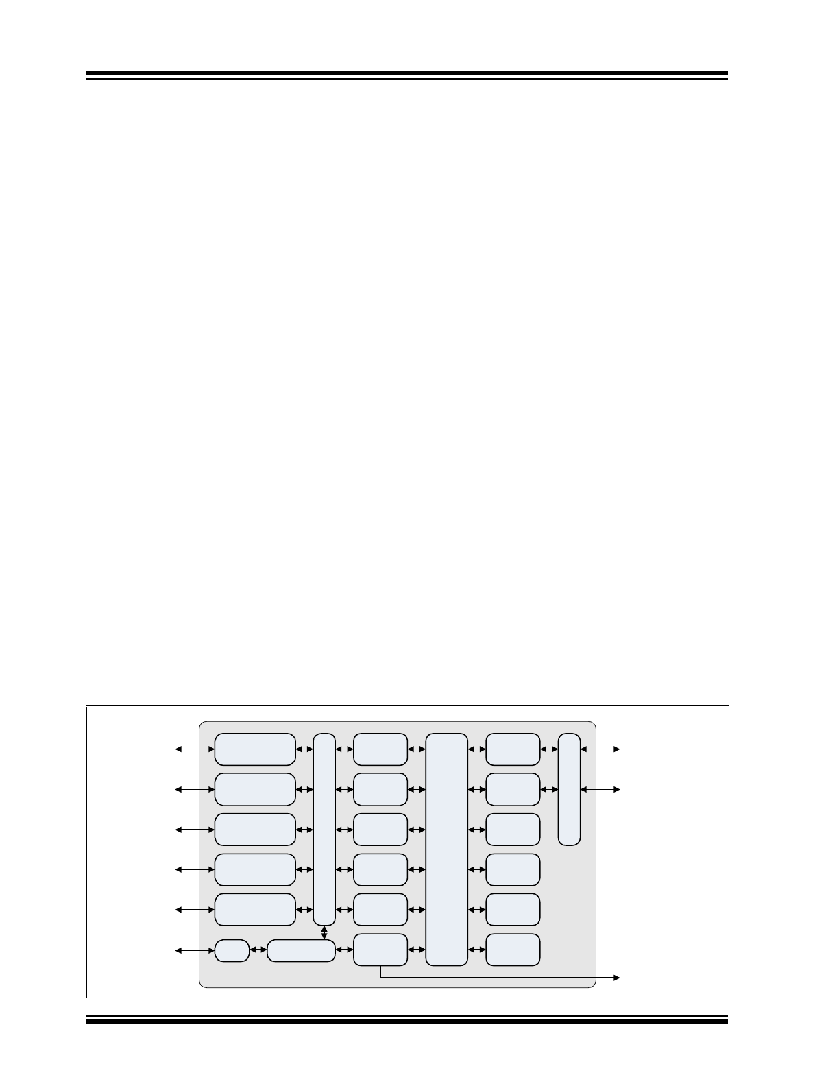
ranges. An internal block diagram of the KSZ8567R is shown in
Figure 2-1
.
FIGURE 2-1:
INTERNAL BLOCK DIAGRAM
KSZ8567R
Port 1
10/100
PHY 1
10/100
PHY 2
10/100
PHY 3
10/100
PHY 4
10/100
PHY 5
Port 2
Port 3
Port 4
Port 5
MAC 1
MAC 2
MAC 3
MAC 4
MAC 5
Sw
it
ch
En
gi
n
e
15
88
&
AV
B
P
roc
e
ss
ing,
Qu
eu
e
Ma
n
ag
e
m
en
t,
QO
S,
Et
c.
Control
Registers
MAC 6
MAC 7
RGMII/MII/RMII
RGMII/MII/RMII
Address
Lookup
MIB
Counters
Frame
Buffers
Queue
Mgmt.
SPI/I
2
C/MIIM
IEEE
15
8
8
/
80
2
.1
A
S
Ti
me
St
am
p
IE
EE
15
8
8
/
80
2
.1
A
S
Ti
m
e
St
a
m
p
IEEE 1588 /
802.1AS Clock
GPIO
Precision
GPIO
2017 - 2018 Microchip Technology Inc.
DS00002328D-page 9
KSZ8567R
3.0
PIN DESCRIPTIONS AND CONFIGURATION
3.1
Pin Assignments
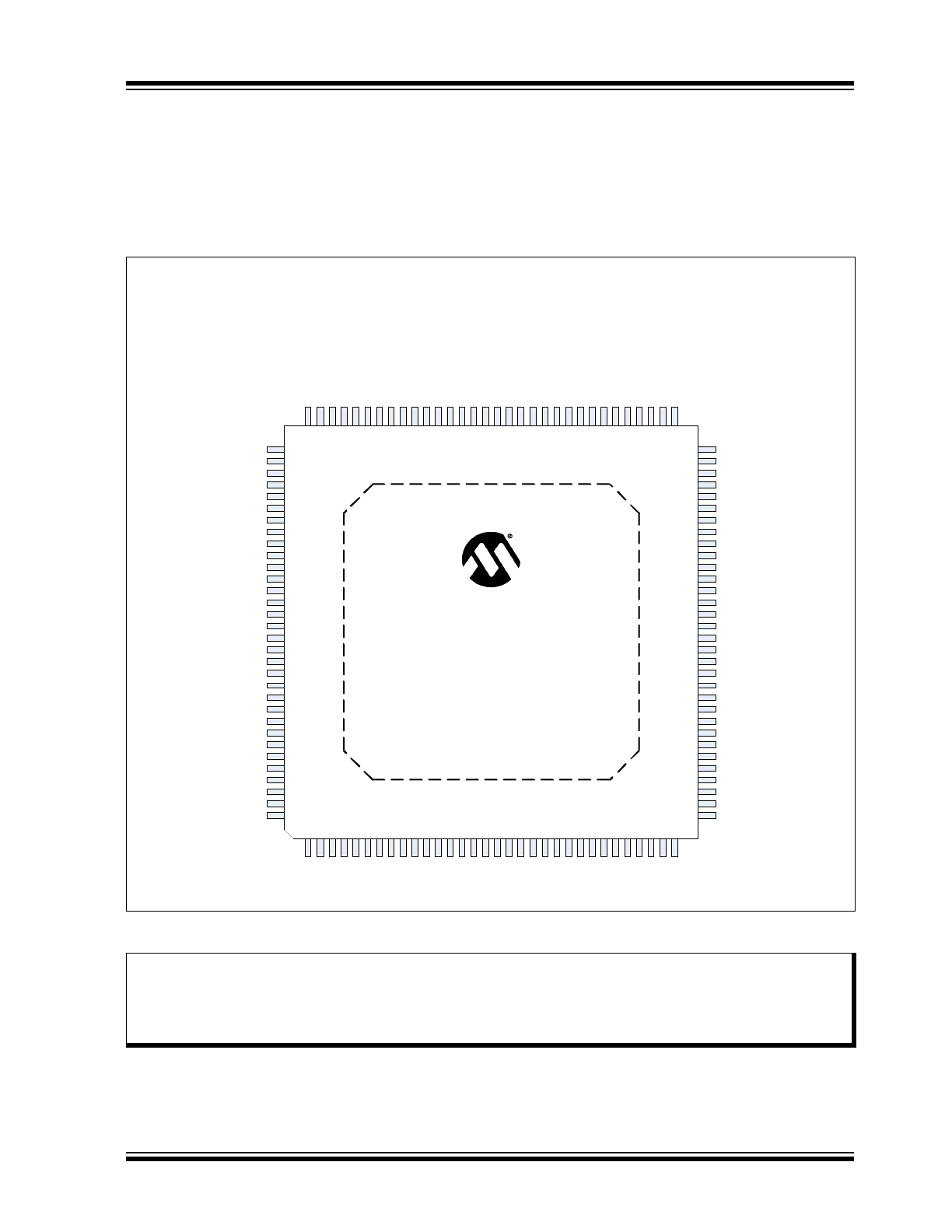
The device pin diagram for the KSZ8567R can be seen in
Figure 3-1
.
Table 3-1
provides a KSZ8567R pin assignment
table. Pin descriptions are provided in
Section 3.2, "Pin Descriptions"
.
FIGURE 3-1:
PIN ASSIGNMENTS (TOP VIEW)
Note:
When an “_N” is used at the end of the signal name, it indicates that the signal is active low. For example,
RESET_N indicates that the reset signal is active low.
The buffer type for each signal is indicated in the “Buffer Type” column of the pin description tables in
Sec-
tion 3.2, "Pin Descriptions"
. A description of the buffer types is provided in
Section 1.2, "Buffer Types"
.
KSZ8567R
128-TQFP-EP
(Top View)
TX
1P
TX
1M
RX
1
P
RX
1
M
NC
NC
NC
NC
TX
2P
TX
2M
AV
DD
L
RX
2
P
RX
2
M
NC
NC
NC
NC
TX
3P
TX
3M
RX
3
P
RX
3
M
NC
NC
NC
NC
R
E
S
ET_N
SY
N
C
L
K
O
IN
T
R
P
_
N
PM
E
_
N
LED
2_1
LED
2_0
GP
IO
_
1
LED
3_1
LED
3_0
LED
4_1
LED
4_0
R
XD7
_
0
R
XD7
_
1
R
XD7
_
2
R
XD7
_
3
CR
S
7
RX
_
E
R
7
R
X
_
D
V
7
/C
RS_
D
V
7
/RX_
C
T
L
7
R
X
_C
LK
7
/R
E
F
C
LK
O
7
TX
D
7_0
TX
D
7_1
TX
D
7_2
TX
D
7_3
CO
L
7
TX
_ER
7
T
X
_
E
N7
/T
X_
C
T
L
7
TX
_C
LK
7/
R
E
F
C
LK
I7
R
XD6
_
0
ISET
XI
XO
GND
NC
NC
AVDDL
NC
NC
RX5M
RX5P
TX5M
TX5P
NC
LED1_1
LED1_0
LED5_1
LED5_0
SCL/MDC
SCS_N
SDI/SDA/MDIO
SDO
TX4P
TX4M
RX4P
RX4M
NC
NC
NC
NC
TX_CLK6/REFCLKI6
TX_EN6/TX_CTL6
TX_ER6
COL6
TXD6_3
TXD6_2
TXD6_1
TXD6_0
RX_CLK6/REFCLKO6
RX_DV6/CRS_DV6/RX_CTL6
RX_ER6
CRS6
RXD6_3
RXD6_2
RXD6_1
33
34
35
36
37
38
39
40
41
42
43
44
45
46
47
48
49
50
51
52
53
54
55
56
57
58
59
60
61
62
63
64
128
127
126
125
124
123
122
121
120
119
118
117
116
115
114
113
112
111
110
109
108
107
106
105
104
103
102
101
100
99
98
97
96
95
94
93
92
91
90
89
88
87
86
85
84
83
82
81
80
79
78
77
76
75
74
73
72
71
70
69
68
67
66
65
1
2
3
4
5
6
7
8
9
10
11
12
13
14
15
16
17
18
19
20
21
22
23
24
25
26
27
28
29
30
31
32
AV
DD
L
AV
DD
L
AV
DD
L
A
VDD
H
AVDDH
AVDDL
AVDDL
AVDDH
A
VDD
H
AVDDH
AVDDL
AVDDH
AVDDH
AVDDL
DVDDL
DVDDL
D
VDD
L
D
VDD
L
DVDDL
DVDDL
GND
GND
GN
D
GND
GND
VDDIO
DV
DD
L
DV
DD
L
VDDIO
V
DDI
O
(Connect exposed pad to ground with a via field)
G N D

KSZ8567R
DS00002328D-page 10
2017 - 2018 Microchip Technology Inc.
Note 3-1
This pin also provides configuration strap functions during hardware/software resets. Refer to
Section
3.2.1, "Configuration Straps"
for additional information.
TABLE 3-1:
PIN ASSIGNMENTS
Pin
Pin Name
Pin
Pin Name
Pin
Pin Name
Pin
Pin Name
1
TX1P
33
AVDDH
65
RXD6_0
(
Note 3-1
)
97
SDO
2
TX1M
34
TX4P
66
TX_CLK7/REFCLKI7
98
SDI/SDA/MDIO
3
AVDDL
35
TX4M
67
TX_EN7/TX_CTL7
99
VDDIO
4
RX1P
36
AVDDL
68
TX_ER7
100
SCS_N
5
RX1M
37
RX4P
69
COL7
101
SCL/MDC
6
NC
38
RX4M
70
TXD7_3
102
LED5_0
7
NC
39
NC
71
TXD7_2
103
LED5_1
(
Note 3-1
)
8
NC
40
NC
72
TXD7_1
104
DVDDL
9
NC
41
AVDDL
73
TXD7_0
105
LED1_0
10
AVDDH
42
NC
74
DVDDL
106
LED1_1
(
Note 3-1
)
11
DVDDL
43
NC
75 RX_CLK7/REFCLKO7 107
GND
12
TX2P
44
AVDDH
76
RX_DV7/CRS_DV7/
RX_CTL7
(
Note 3-1
)
108
NC
13
TX2M
45
DVDDL
77
VDDIO
109
GND
14
AVDDL
46
GND
78
RX_ER7
110
DVDDL
15
RX2P
47
GND
79
CRS7
111
AVDDH
16
RX2M
48
TX_CLK6/REFCLKI6
80
RXD7_3
(
Note 3-1
)
112
TX5P
17
NC
49
TX_EN6/TX_CTL6
81
RXD7_2
(
Note 3-1
)
113
TX5M
18
NC
50
TX_ER6
82
RXD7_1
(
Note 3-1
)
114
AVDDL
19
AVDDL
51
COL6
83
RXD7_0
(
Note 3-1
)
115
RX5P
20
NC
52
TXD6_3
84
GND
116
RX5M
21
NC
53
TXD6_2
85
LED4_0
(
Note 3-1
)
117
NC
22
AVDDH
54
TXD6_1
86
LED4_1
(
Note 3-1
)
118
NC
23
DVDDL
55
TXD6_0
87
DVDDL
119
AVDDL
24
TX3P
56
DVDDL
88
LED3_0
120
NC
25
TX3M
57 RX_CLK6/REFCLKO6 89
LED3_1
(
Note 3-1
)
121
NC
26
RX3P
58
RX_DV6/CRS_DV6/
RX_CTL6
90
GPIO_1
122
AVDDH
27
RX3M
59
RX_ER6
91
LED2_0
(
Note 3-1
)
123
GND
28
NC
60
CRS6
92
LED2_1
(
Note 3-1
)
124
AVDDL
29
NC
61
VDDIO
93
PME_N
125
XO
30
AVDDL
62
RXD6_3
(
Note 3-1
)
94
INTRP_N
126
XI
31
NC
63
RXD6_2
(
Note 3-1
)
95
SYNCLKO
127
ISET
32
NC
64
RXD6_1
(
Note 3-1
)
96
RESET_N
128
AVDDH
Exposed Pad Must be Connected to GND