

2016 Microchip Technology Inc.
DS00002298A-page 1
Features
• Single-Chip 10BASE-T/100BASE-TX IEEE 802.3
Compliant Ethernet Transceiver
• RMII V1.2 Interface Support with a 50 MHz Refer-
ence Clock Output to MAC, and an Option to
Input a 50 MHz Reference Clock
• RMII Back-to-Back Mode Support for a 100 Mbps
Copper Repeater
• MDC/MDIO Management Interface for PHY Reg-
ister Configuration
• Programmable Interrupt Output
• LED Outputs for Link and Activity Status Indica-
tion
• On-Chip Termination Resistors for the Differential
Pairs
• Baseline Wander Correction
• HP Auto MDI/MDI-X to Reliably Detect and Cor-
rect Straight-Through and Crossover Cable Con-
nections with Disable and Enable Option
• Auto-Negotiation to Automatically Select the
Highest Link-Up Speed (10/100 Mbps) and
Duplex (Half/Full)
• Energy Efficient Ethernet (EEE) Support with
Low-Power Idle (LPI) Mode for 100BASE-TX and
Transmit Amplitude Reduction with 10BASE-TE
Option
• Wake-on-LAN (WoL) Support with Either Magic
Packet, Link Status Change, or Robust Custom-
Packet Detection
• LinkMD
®
TDR-Based Cable Diagnostics to Iden-
tify Faulty Copper Cabling
• HBM ESD Rating (6 kV)
• Parametric NAND Tree Support for Fault Detec-
tion Between Chip I/Os and the Board
• Loopback Modes for Diagnostics
• Power-Down and Power-Saving Modes
• Single 3.3V Power Supply with V
DD
I/O Options
for 1.8V, 2.5V, or 3.3V
• Built-In 1.2V Regulator for Core
• Available in 24-Pin (4 mm × 4 mm) QFN Package
Target Applications
• Game Consoles
• IP Phones
• IP Set-Top Boxes
• IP TVs
• LOM
• Printers
KSZ8091RNA/RND
10BASE-T/100BASE-TX PHY
with RMII and EEE Support

KSZ8091RNA/RND
DS00002298A-page 2
2016 Microchip Technology Inc.
TO OUR VALUED CUSTOMERS
It is our intention to provide our valued customers with the best documentation possible to ensure successful use of your Microchip
products. To this end, we will continue to improve our publications to better suit your needs. Our publications will be refined and
enhanced as new volumes and updates are introduced.
If you have any questions or comments regarding this publication, please contact the Marketing Communications Department via
E-mail at
docerrors@microchip.com
. We welcome your feedback.
Most Current Data Sheet
To obtain the most up-to-date version of this data sheet, please register at our Worldwide Web site at:
http://www.microchip.com
You can determine the version of a data sheet by examining its literature number found on the bottom outside corner of any page.
The last character of the literature number is the version number, (e.g., DS30000000A is version A of document DS30000000).
Errata
An errata sheet, describing minor operational differences from the data sheet and recommended workarounds, may exist for cur-
rent devices. As device/documentation issues become known to us, we will publish an errata sheet. The errata will specify the
revision of silicon and revision of document to which it applies.
To determine if an errata sheet exists for a particular device, please check with one of the following:
• Microchip’s Worldwide Web site;
http://www.microchip.com
• Your local Microchip sales office (see last page)
When contacting a sales office, please specify which device, revision of silicon and data sheet (include -literature number) you are
using.
Customer Notification System
Register on our web site at
www.microchip.com
to receive the most current information on all of our products.

2016 Microchip Technology Inc.
DS00002298A-page 3
KSZ8091RNA/RND
Table of Contents
1.0 Introduction ..................................................................................................................................................................................... 4
2.0 Pin Description and Configuration .................................................................................................................................................. 5
3.0 Functional Description .................................................................................................................................................................. 10
4.0 Register Descriptions .................................................................................................................................................................... 29
5.0 Operational Characteristics ........................................................................................................................................................... 45
6.0 Electrical Characteristics ............................................................................................................................................................... 46
7.0 Timing Diagrams ........................................................................................................................................................................... 48
8.0 Reset Circuit ................................................................................................................................................................................. 52
9.0 Reference Circuits — LED Strap-In Pins ...................................................................................................................................... 53
10.0 Reference Clock - Connection and Selection ............................................................................................................................. 54
11.0 Magnetic - Connection and Selection ......................................................................................................................................... 55
12.0 Package Outline .......................................................................................................................................................................... 57
Appendix A: Data Sheet Revision History ........................................................................................................................................... 58
The Microchip Web Site ...................................................................................................................................................................... 59
Customer Change Notification Service ............................................................................................................................................... 59
Customer Support ............................................................................................................................................................................... 59
Product Identification System ............................................................................................................................................................. 60
KSZ8091RNA/RND
DS00002298A-page 4
2016 Microchip Technology Inc.
1.0
INTRODUCTION
1.1
General Description
The KSZ8091RNA is a single-supply 10BASE-T/100BASE-TX Ethernet physical-layer transceiver for transmission and
reception of data over standard CAT-5 unshielded twisted pair (UTP) cable.
The KSZ8091RNA is a highly integrated PHY solution. It reduces board cost and simplifies board layout by using on-
chip termination resistors for the differential pairs and by integrating a low-noise regulator to supply the 1.2V core, and
by offering a flexible 1.8/2.5/3.3V digital I/O interface.
The KSZ8091RNA offers the Reduced Media Independent Interface (RMII) for direct connection with RMII-compliant
Ethernet MAC processors and switches.
As the power-up default, the KSZ8091RNA uses a 25 MHz crystal to generate all required clocks, including the 50 MHz
RMII reference clock output for the MAC. The KSZ8091RND takes in the 50 MHz RMII reference clock as the power-
up default.
Energy Efficient Ethernet (EEE) provides further power saving during idle traffic periods and Wake-On-LAN (WOL) pro-
vides a mechanism for the KSZ8091RNA to wake up a system that is in standby power mode.
The KSZ8091RNA and KSZ8091RND are available in 24-pin, lead-free QFN packages.
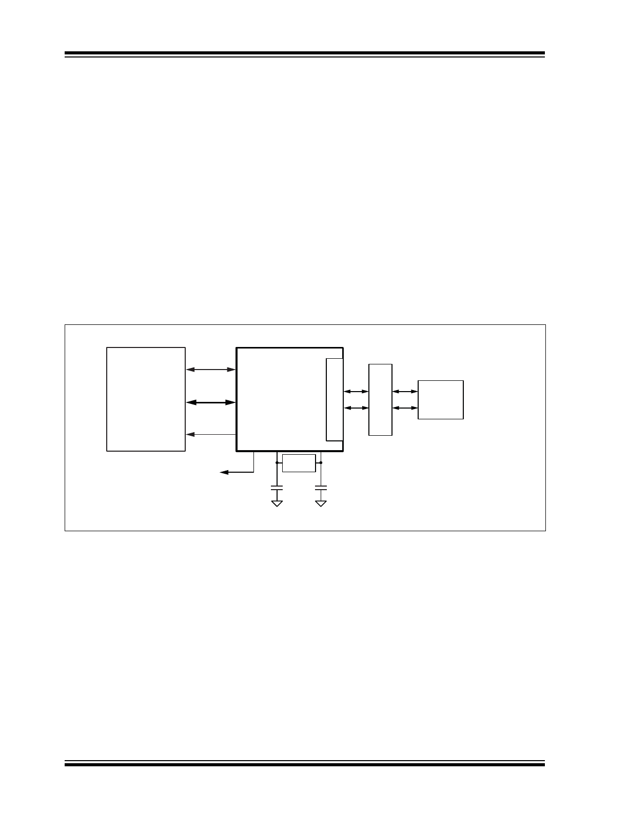
FIGURE 1-1:
SYSTEM BLOCK DIAGRAM
KSZ8091RNA/RND
MAGNETICS
RJ-45
CONNECTOR
MEDIA TYPES:
10BASE-T
100BASE-TX
ON-CHIP TERMINATION
RESISTORS
RMII
MDC/MDIO
MANAGEMENT
XO
XI
25MHz
XTAL
22pF
22pF
10/100Mbps
RMII MAC
50MHz
REF_CLK
PME_N
(SYSTEM
POWER
CIRCUIT)
2016 Microchip Technology Inc.
DS00002275A-page 5
KSZ8091RNA/RND
2.0
PIN DESCRIPTION AND CONFIGURATION
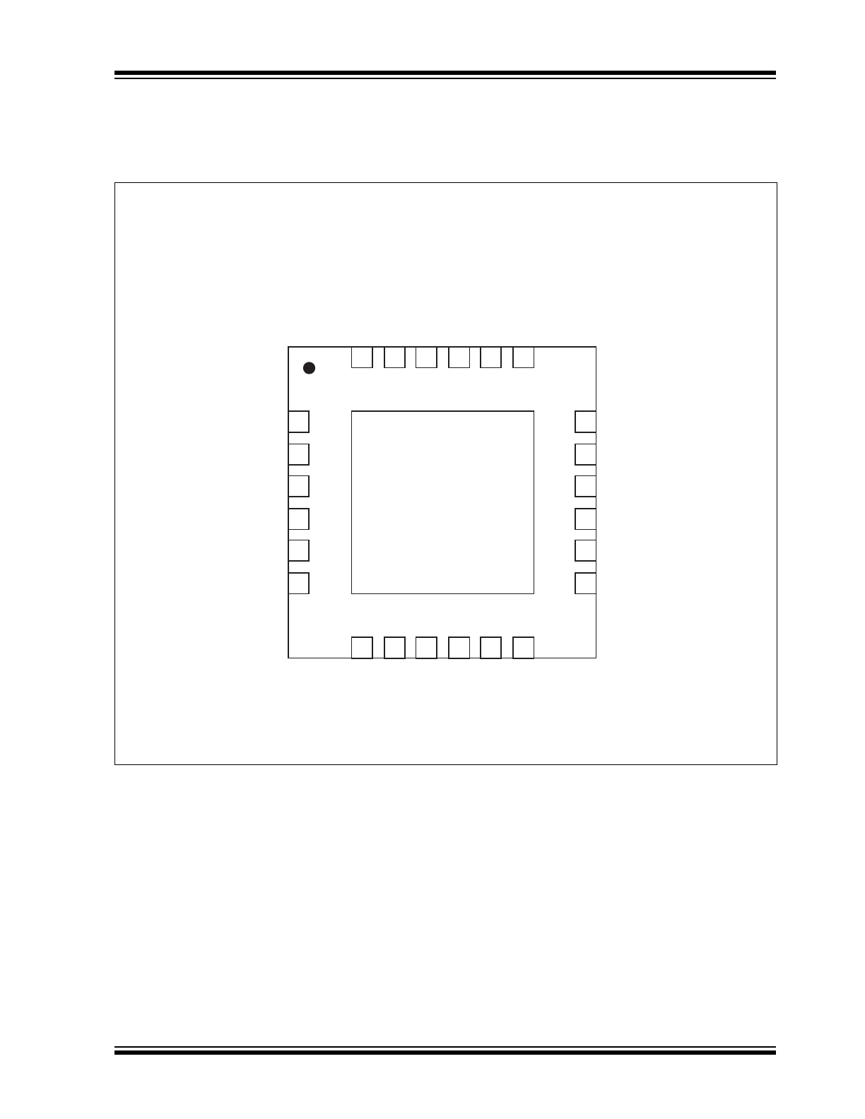
FIGURE 2-1:
24-PIN 4 MM X 4 MM QFN ASSIGNMENT (TOP VIEW)
1
2
3
4
5
6
18
17
16
15
14
13
24
23
22
21
20
19
7
8
9
10
11
12
PADDLE GROUND
(ON BOTTOM OF CHIP)
VDD_1.2
VDDA_3.3
RXM
RXP
TXM
TXP
INTRP/
PME_N2
RXER/
PME_EN
REF_CLK
CRS_DV/
PHYAD[1:0]
VDDIO
RXD0
RST#
LED0/PME_N1
/
ANEN_SPEED
GND
TXD1
TXD0
TXEN
XO
XI
REXT
MDIO
MDC
RXD1

KSZ8091RNA/RND
DS00002275A-page 6
2016 Microchip Technology Inc.
TABLE 2-1:
SIGNALS - KSZ8091RNA/RND
Pin
Number
Pin
Name
Type
Note
2-1
Description
1
VDD_1.2
P
1.2V Core V
DD
(power supplied by KSZ8091RNA/KSZ8091RND). Decouple
with 2.2 µF and 0.1 µF capacitors to ground.
2
VDDA_3.3
P
3.3V analog V
DD
.
3
RXM
I/O
Physical receive or transmit signal (– differential).
4
RXP
I/O
Physical receive or transmit signal (+ differential).
5
TXM
I/O
Physical transmit or receive signal (– differential).
6
TXP
I/O
Physical transmit or receive signal (+ differential).
7
XO
O
Crystal Feedback for 25 MHz Crystal. This pin is a no connect if an oscillator
or external clock source is used.
8
XI
I
RMII – 25 MHz Mode: 25 MHz ±50 ppm Crystal/Oscillator/External Clock
Input
RMII – 50 MHz Mode: 50 MHz ±50 ppm Oscillator/External Clock Input
For unmanaged mode (power-up default setting),
KSZ8091RNA takes in the 25 MHz crystal/clock on this pin.
KSZ8091RND takes in the 50 MHz clock on this pin.
After power-up, both the KSZ8091RNA and KSZ8091RND can be pro-
grammed to either the 25 MHz mode or 50 MHz mode using PHY Register
1Fh, Bit [7].
See REF_CLK (Pin 16).
9
REXT
I
Set PHY Transmit Output Current
Connect a 6.49 kΩ resistor to ground on this pin.
10
MDIO
Ipu/
Opu
Management Interface (MII) Data I/O. This pin has a weak pull-up, is open-
drain, and requires an external 1.0 kΩ pull-up resistor.
11
MDC
Ipu
Management Interface (MII) Clock Input. This clock pin is synchronous to
the MDIO data pin.
12
RXD1
Ipd/O
RMII Receive Data Output[1] (
Note 2-2
).
13
RXD0
Ipu/O
RMII Receive Data Output[0] (
Note 2-2
).
14
VDDIO
P
3.3V, 2.5V, or 1.8V digital V
DD
.
15
CRS_DV /
PHYAD[1:0]
Ipd/O
RMII Mode: Carrier Sense/Receive Data Valid output
Config Mode: The pull-up/pull-down value is latched as PHYAD[1:0] at the
de-assertion of reset.
See the
Strap-In Options - KSZ8091RNA/RND
section for details.

2016 Microchip Technology Inc.
DS00002275A-page 7
KSZ8091RNA/RND
16
REF_CLK
Ipd/O
RMII – 25 MHz Mode: This pin provides the 50 MHz RMII reference clock
output to the MAC.
RMII – 50 MHz Mode: This pin is a no connect.
For unmanaged mode (power-up default setting):
• KSZ8091RNA is in RMII – 25 MHz mode and outputs the 50 MHz RMII
reference clock on this pin.
• KSZ8091RND is in RMII – 50 MHz mode and does not use this pin.
After power-up, both KSZ8091RNA and KSZ8091RND can be programmed
to either 25 MHz mode or 50 MHz mode using PHY Register 1Fh, Bit [7].
See also XI (Pin 8).
17
RXER /
PME_EN
Ipd/O
RMII Mode: RMII Receive Error Output
Config Mode: The pull-up/pull-down value is latched as PME_EN at the de-
assertion of reset. See the
Strap-In Options - KSZ8091RNA/RND
section for
details.
18
INTRP/
PME_N2
Ipu/
Opu
Interrupt Output: Programmable interrupt output, with Register 1Bh as the
Interrupt Control/Status register, for programming the interrupt conditions
and reading the interrupt status. Register 1Fh, Bit [9] sets the interrupt output
to active low (default) or active high.
PME_N Output: Programmable PME_N output (pin option 2). When
asserted low, this pin signals that a WOL event has occurred.
This pin has a weak pull-up and is an open-drain.
For Interrupt (when active low) and PME functions, this pin requires an
external 1.0 kΩ pull-up resistor to V
DDIO
(digital V
DD
).
19
TXEN
I
RMII Transmit Enable Input
20
TXD0
I
RMII Transmit Data Input[0] (
Note 2-3
)
21
TXD1
I/O
RMII Mode: RMII Transmit Data Input[1] (
Note 2-3
)
NAND Tree Mode: NAND Tree Output
22
GND
GND
Ground
TABLE 2-1:
SIGNALS - KSZ8091RNA/RND (CONTINUED)
Pin
Number
Pin
Name
Type
Note
2-1
Description
KSZ8091RNA/RND
DS00002275A-page 8
2016 Microchip Technology Inc.
Note 2-1
P = power supply
GND = ground
I = input
O = output
I/O = bi-directional
Ipu = Input with internal pull-up (see
Electrical Characteristics
for value).
Ipd = Input with internal pull-down (see
Electrical Characteristics
for value).
Ipu/O = Input with internal pull-up (see
Electrical Characteristics
for value) during power-up/reset;
output pin otherwise.
Ipd/O = Input with internal pull-down (see
Electrical Characteristics
for value) during power-up/reset;
output pin otherwise.
Ipu/Opu = Input with internal pull-up (see
Electrical Characteristics
for value) and output with internal
pull-up (see
Electrical Characteristics
for value).
Note 2-2
RMII RX Mode: The RXD[1:0] bits are synchronous with the 50 MHz RMII Reference Clock. For each
clock period in which CRS_DV is asserted, two bits of recovered data are sent by the PHY to the
MAC.
Note 2-3
RMII TX Mode: The TXD[1:0] bits are synchronous with the 50 MHz RMII Reference Clock. For each
clock period in which TXEN is asserted, two bits of data are received by the PHY from the MAC.
23
LED0/
PME_N1/
ANEN_SPEED
Ipu/O
LED Output: Programmable LED0 output
PME_N Output: Programmable PME_N Output (pin option 1). When
asserted low, this pin signals that a WOL event has occurred. In this mode,
this pin has a weak pull-up, is an open-drain, and requires an external
1.0 kΩ pull-up resistor to V
DDIO
(digital V
DD
).
Config Mode: Latched as Auto-Negotiation enable (Register 0h, Bit [12]) and
Speed (Register 0h, Bit [13]) at the de-assertion of reset. See the Strapping
Options section for details.
The LED0 pin is programmable using Register 1Fh, Bits [5:4], and is defined
as follows:
LED Mode = [00]
Link/Activity
Pin State
LED Definition
No Link
High
OFF
Link
Low
ON
Activity
Toggle
Blinking
LED Mode = [01]
Link/Activity
Pin State
LED Definition
No Link
High
OFF
Link
Low
ON
LED Mode = [10], [11]
‘ Reserved
24
RST#
Ipu
Chip Reset (Active Low)
PADDLE
GND
GND
Ground
TABLE 2-1:
SIGNALS - KSZ8091RNA/RND (CONTINUED)
Pin
Number
Pin
Name
Type
Note
2-1
Description

2016 Microchip Technology Inc.
DS00002275A-page 9
KSZ8091RNA/RND
2.1
Strap-In Options - KSZ8091RNA/RND
The PHYAD[1:0] and PME_EN strap-in pins are latched at the de-assertion of reset. In some systems, the RMII MAC
receive input pins may drive high/low during power-up or reset, and consequently cause the PHYAD[1:0] and PME_EN
strap-in pins, shared pin with the RMII CRS_DV and RXER signals respectively, to be latched to the unintended high/
low state. In this case, an external pull-up (4.7 kΩ) or pull-down (1.0 kΩ) should be added on the PHYAD[1:0] and
PME_EN strap-in pins to ensure that the intended value is strapped-in correctly.
Note 2-4
Ipu/O = Input with internal pull-up (see
Electrical Characteristics
for value) during power-up/reset;
output pin otherwise.
Ipd/O = Input with internal pull-down (see
Electrical Characteristics
for value) during power-up/reset;
output pin otherwise.
TABLE 2-2:
STRAP-IN OPTIONS - KSZ8091RNA/RND
Pin Number
Pin Name
Type
Note 2-4
Description
15
PHYAD[1:0]
Ipd/O
The PHY Address is latched at the de-assertion of reset and is con-
figurable to either one of the following two values:
Pull-up = PHY Address is set to 00011b (3h)
Pull-down (default) = PHY Address is set to 00000b (0h)
PHY Address 0 is assigned by default as the broadcast PHY
address, but it can be assigned as a unique PHY address after writ-
ing a ‘1’ to Register 16h, Bit [9].
PHY Address bits [4:2] are set to 000 by default.
17
PME_EN
Ipd/O
PME Output for Wake-On-LAN
Pull-up = Enable
Pull-down (default) = Disable
At the de-assertion of reset, this pin value is latched into Register
16h, Bit [15].
23
ANEN_SPEED
Ipu/O
Auto-Negotiation Enable and Speed Mode
Pull-up (default) = Enable Auto-Negotiation and set 100 Mbps Speed
Pull-down = Disable Auto-Negotiation and set 10 Mbps Speed
At the de-assertion of reset, this pin value is latched into Register 0h,
Bit [12] for Auto-Negotiation enable/disable, Register 0h, Bit [13] for
the Speed select, and Register 4h (Auto-Negotiation Advertisement)
for the Speed capability support.

KSZ8091RNA/RND
DS00002298A-page 10
2016 Microchip Technology Inc.
3.0
FUNCTIONAL DESCRIPTION
The KSZ8091RNA is an integrated single 3.3V supply Fast Ethernet transceiver. It is fully compliant with the IEEE 802.3
Specification, and reduces board cost and simplifies board layout by using on-chip termination resistors for the two dif-
ferential pairs and by integrating the regulator to supply the 1.2V core.
On the copper media side, the KSZ8091RNA supports 10BASE-T and 100BASE-TX for transmission and reception of
data over a standard CAT-5 unshielded twisted pair (UTP) cable, and HP Auto MDI/MDI-X for reliable detection of and
correction for straight-through and crossover cables.
On the MAC processor side, the KSZ8091RNA offers the Reduced Media Independent Interface (RMII) for direct con-
nection with RMII-compliant Ethernet MAC processors and switches
The MII management bus option gives the MAC processor complete access to the KSZ8091RNA control and status
registers. Additionally, an interrupt pin eliminates the need for the processor to poll for PHY status change.
As the power-up default, the KSZ8091RNA uses a 25 MHz crystal to generate all required clocks, including the 50 MHz
RMII reference clock output for the MAC. The KSZ8091RND version uses the 50 MHz RMII reference clock as the
power-up default.
The KSZ8091RNA/RND is used to refer to both KSZ8091RNA and KSZ8091RND versions in this datasheet.
3.1
10BASE-T/100BASE-TX Transceiver
3.1.1
100BASE-TX TRANSMIT
The 100BASE-TX transmit function performs parallel-to-serial conversion, 4B/5B encoding, scrambling, NRZ-to-NRZI
conversion, and MLT3 encoding and transmission.
The circuitry starts with a parallel-to-serial conversion, which converts the MII/RMII data from the MAC into a 125 MHz
serial bit stream. The data and control stream is then converted into 4B/5B coding and followed by a scrambler. The
serialized data is further converted from NRZ-to-NRZI format, and then transmitted in MLT3 current output. The output
current is set by an external 6.49 kΩ 1% resistor for the 1:1 transformer ratio.
The output signal has a typical rise/fall time of 4ns and complies with the ANSI TP-PMD standard regarding amplitude
balance, overshoot, and timing jitter. The wave-shaped 10BASE-T output is also incorporated into the 100BASE-TX
transmitter.
3.1.2
100BASE-TX RECEIVE
The 100BASE-TX receiver function performs adaptive equalization, DC restoration, MLT3-to-NRZI conversion, data and
clock recovery, NRZI-to-NRZ conversion, de-scrambling, 4B/5B decoding, and serial-to-parallel conversion.
The receiving side starts with the equalization filter to compensate for inter-symbol interference (ISI) over the twisted
pair cable. Because the amplitude loss and phase distortion is a function of the cable length, the equalizer must adjust
its characteristics to optimize performance. In this design, the variable equalizer makes an initial estimation based on
comparisons of incoming signal strength against some known cable characteristics, then tunes itself for optimization.
This is an ongoing process and self-adjusts against environmental changes such as temperature variations.
Next, the equalized signal goes through a DC-restoration and data-conversion block. The DC-restoration circuit com-
pensates for the effect of baseline wander and improves the dynamic range. The differential data-conversion circuit con-
verts MLT3 format back to NRZI. The slicing threshold is also adaptive.
The clock-recovery circuit extracts the 125 MHz clock from the edges of the NRZI signal. This recovered clock is then
used to convert the NRZI signal to NRZ format. This signal is sent through the de-scrambler, then the 4B/5B decoder.
Finally, the NRZ serial data is converted to MII/RMII format and provided as the input data to the MAC.
3.1.3
SCRAMBLER/DE-SCRAMBLER (100BASE-TX ONLY)
The scrambler spreads the power spectrum of the transmitted signal to reduce electromagnetic interference (EMI) and
baseline wander. The de-scrambler recovers the scrambled signal.
3.1.4
10BASE-T TRANSMIT
The 10BASE-T drivers are incorporated with the 100BASE-TX drivers to allow for transmission using the same mag-
netic. The drivers perform internal wave-shaping and pre-emphasis, and output 10BASE-T signals with a typical ampli-
tude of 2.5V peak for standard 10BASE-T mode and 1.75V peak for energy-efficient 10BASE-Te mode. The 10BASE-
T/10BASE-Te signals have harmonic contents that are at least 27 dB below the fundamental frequency when driven by
an all-ones Manchester-encoded signal.