

2016-2018 Microchip Technology Inc.
DS00002197E-page 1
Highlights
• Single-Chip Ethernet Physical Layer Transceiver
(PHY)
• Quiet-Wire
®
technology to reduce line emissions
and enhance immunity
• Ultra-Deep Sleep standby mode
• AEC-Q100 Grade 2 Automotive Qualified
Target Applications
• Industrial Control
• Vehicle On-Board Diagnostics (OBD)
• Automotive Gateways
• Camera and Sensor Networking
• Infotainment
Key Benefits
• Quiet-Wire Programmable EMI Filter
• RMII Interface with MDC/MDIO Management
Interface for Register Configuration
• On-Chip Termination Resistors for Differential
Pairs
• LinkMD
®
+ Receive Signal Quality Indicator
• Fast Start-Up and Link
• Ultra Deep Sleep Standby Mode; CPU or Signal
Detect Activated
• Loopback Modes for Diagnostics
• Programmable Interrupt Output
KSZ8061RNB/RND
10BASE-T/100BASE-TX Physical Layer
Transceiver

KSZ8061RNB/RND
DS00002197E-page 2
2016-2018 Microchip Technology Inc.
TO OUR VALUED CUSTOMERS
It is our intention to provide our valued customers with the best documentation possible to ensure successful use of your Microchip
products. To this end, we will continue to improve our publications to better suit your needs. Our publications will be refined and
enhanced as new volumes and updates are introduced.
If you have any questions or comments regarding this publication, please contact the Marketing Communications Department via
E-mail at
docerrors@microchip.com
. We welcome your feedback.
Most Current Data Sheet
To obtain the most up-to-date version of this data sheet, please register at our Worldwide Web site at:
http://www.microchip.com
You can determine the version of a data sheet by examining its literature number found on the bottom outside corner of any page.
The last character of the literature number is the version number, (e.g., DS30000000A is version A of document DS30000000).
Errata
An errata sheet, describing minor operational differences from the data sheet and recommended workarounds, may exist for cur-
rent devices. As device/documentation issues become known to us, we will publish an errata sheet. The errata will specify the
revision of silicon and revision of document to which it applies.
To determine if an errata sheet exists for a particular device, please check with one of the following:
• Microchip’s Worldwide Web site;
http://www.microchip.com
• Your local Microchip sales office (see last page)
When contacting a sales office, please specify which device, revision of silicon and data sheet (include -literature number) you are
using.
Customer Notification System
Register on our web site at
www.microchip.com
to receive the most current information on all of our products.

2016-2018 Microchip Technology Inc.
DS00002197E-page 3
KSZ8061RNB/RND
Table of Contents
1.0 Introduction ..................................................................................................................................................................................... 4
2.0 Pin Description and Configuration .................................................................................................................................................. 5
3.0 Functional Description .................................................................................................................................................................... 9
4.0 Register Map ................................................................................................................................................................................. 25
5.0 Operational Characteristics ........................................................................................................................................................... 38
6.0 Electrical Characteristics ............................................................................................................................................................... 39
7.0 Timing Diagrams ........................................................................................................................................................................... 42
8.0 Reset Circuit ................................................................................................................................................................................. 46
9.0 Reference Clock Connection and Selection - KSZ8061RNB ........................................................................................................ 47
10.0 Reference Clock Connection - KSZ8061RND ............................................................................................................................ 48
11.0 Package Outlines ........................................................................................................................................................................ 49
Appendix A: Data Sheet Revision History ........................................................................................................................................... 51
The Microchip Web Site ...................................................................................................................................................................... 52
Customer Change Notification Service ............................................................................................................................................... 52
Customer Support ............................................................................................................................................................................... 52
Product Identification System ............................................................................................................................................................. 53
KSZ8061RNB/RND
DS00002197E-page 4
2016-2018 Microchip Technology Inc.
1.0
INTRODUCTION
1.1
General Description
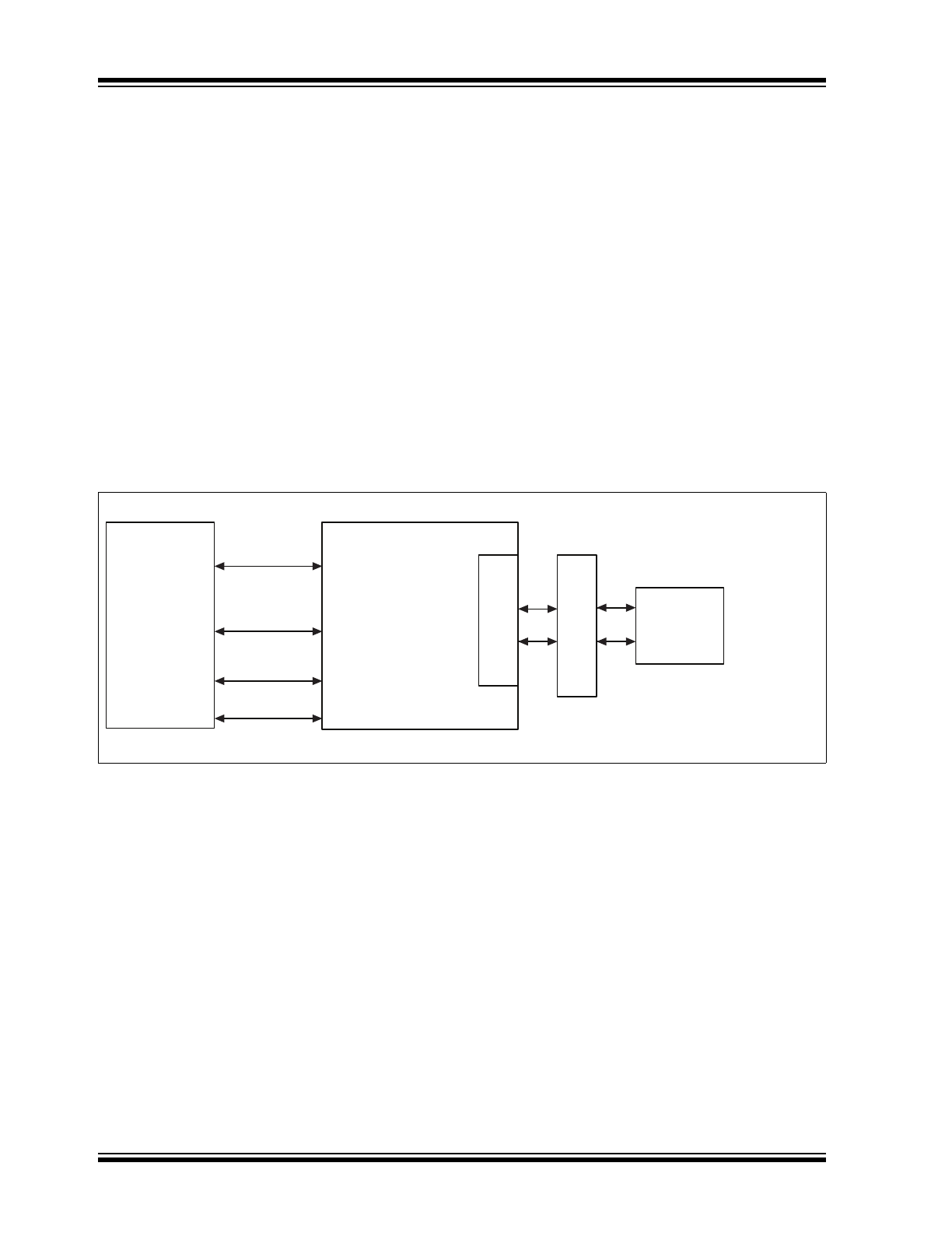
The KSZ8061RNB/RND is a single-chip 10BASE-T/100BASE-TX Ethernet physical layer transceiver for transmission
and reception of data over an unshielded twisted pair (UTP) cable.
The KSZ8061RNB/RND features Quiet-Wire
®
internal filtering to reduce line emissions. It is ideal for applications, such
as automotive or industrial networks, where stringent radiated emission limits must be met. Quiet-Wire can utilize low-
cost unshielded cable, where previously only shielded cable solutions were possible. The KSZ8061RNB/RND also fea-
tures enhanced immunity to environmental EM noise.
The KSZ8061RNB/RND features a Reduced Media Independent Interface (RMII) for direct connection with RMII-com-
pliant Ethernet MAC processors and switches.
The KSZ8061RNB generates a 50-MHz RMII reference clock for use by the connected MAC device. In contrast, the
KSZ8061RND receives the 50-MHz RMII reference clock as an input.
The KSZ8061RNB/RND meets Automotive AEC-Q100 and EMC requirements, with an extended temperature range of
-40°C to +105°C. It is supplied in 32-pin, 5 mm × 5 mm QFN and WQFN packages.
The KSZ8061MNX and KSZ8061MNG devices have an MII interface and are described in a separate data sheet.
FIGURE 1-1:
SYSTEM BLOCK DIAGRAM
Quiet-WIRE
®
FIL
TERING
KSZ8061
MAGNETICS
RJ-45
CONNECTOR
MEDIA TYPES:
10BASE-T
100BASE-TX
10/100 Mbps
RMII MAC
RMII
MDC/MDIO
MANAGEMENT
INTRP
SIGNAL DETECT
2016-2018 Microchip Technology Inc.
DS00002197E-page 5
KSZ8061RNB/RND
2.0
PIN DESCRIPTION AND CONFIGURATION
FIGURE 2-1:
32-QFN PIN ASSIGNMENT (TOP VIEW)
TABLE 2-1:
SIGNALS
Pin Number
Name
Buffer
Type
Note
Description
1
XI
I
KSZ8061RNB: 25-MHz Crystal/Oscillator/External Clock Input. This
input references the AVDDH power supply.
KSZ8061RND: 50-MHz RMII Reference Clock Input. This input refer-
ences the AVDDH power supply.
2
XO
O
KSZ8061RNB: Crystal feedback for 25-MHz crystal. This pin is a no
connect if oscillator or external clock source is used.
KSZ8061RND: This pin is unused. Leave it unconnected.
3
AVDDH
PWR
3.3V Supply for analog TX drivers and XI/XO oscillator circuit.
4
TXP
I/O
Physical transmit or receive signal (+ differential)
Transmit when in MDI mode; Receive when in MDI-X mode.
5
TXM
I/O
Physical transmit or receive signal (– differential)
Transmit when in MDI mode; Receive when in MDI-X mode.
6
RXP
I/O
Physical receive or transmit signal (+ differential)
Receive when in MDI mode; Transmit when in MDI-X mode.
7
RXM
I/O
Physical receive or transmit signal (‒ differential)
Receive when in MDI mode; Transmit when in MDI-X mode.
8
AVDDL
PWR
1.2V (nominal) supply for analog core
9
VDDL
PWR
1.2V (nominal) supply for digital core
10
MDIO
IPU/OPU
Management Interface (MIIM) Data I/O
This pin has a weak pull-up, is open-drain like, and requires an external
1-kΩ pull-up resistor.
XI
XO
AVDDH
TXP
TXM
RXP
RXM
AVDDL
CRS_DV
RXER
MDC
MDIO
VDDL
PHY
A
D0
VDDIO
PHY
A
D1
Bottom paddle is GND
1
2
3
4
5
6
7
8
9
10 11 12 13 14 15 16
24
23
22
21
20
19
18
17
32 31 30 29 28 27 26 25
LED0
TXD1
TXD0
TXEN
LED1
REF_CLK
RXD0
RXD1
RESET#
INTRP
VDDL
REXT
SIGDET
CONFIG1
DNU
DNU

KSZ8061RNB/RND
DS00002197E-page 6
2016-2018 Microchip Technology Inc.
11
MDC
IPU
Management Interface (MIIM) Clock Input
This clock pin is synchronous to the MDIO data pin.
12
RXER / QWF
IPD/O
RMII Receive Error Output
Config Mode: The pull-up or pull-down value is latched as QWF at the
deassertion of reset. See
Table 2-2, "Strap-in Options"
for details.
13
CRS_DV /
CONFIG2
IPD/O
RMII Carrier Sense/Receive Data Valid Output
Config Mode: The pull-up or pull-down value is latched as CONFIG2 at
the deassertion of reset. See
Table 2-2, "Strap-in Options"
for details.
14
PHYAD0
IPU/O
No function during normal operation
Config Mode: The pull-up or pull-down value is latched as PHYADDR[0]
at the deassertion of reset. See
Table 2-2, "Strap-in Options"
for details.
15
VDDIO
PWR
3.3V or 2.5V supply for digital I/O
16
PHYAD1
IPD/O
No function during normal operation
Config Mode: The pull-up or pull-down value is latched as PHYADDR[1]
at the deassertion of reset. See
Table 2-2, "Strap-in Options"
for details.
17
RXD1 /
PHYAD2
IPD/O
RMII Receive Data Output[1] (
Note 2-2
)
Config Mode: The pull-up or pull-down value is latched as PHYADDR[2]
at the deassertion of reset. See
Table 2-2, "Strap-in Options"
for details.
18
RXD0 /
AUTONEG
IPU/O
RMII Receive Data Output[0] (
Note 2-2
)
Config Mode: The pull-up or pull-down value is latched as AUTONEG at
the deassertion of reset. See
Table 2-2, "Strap-in Options"
for details.
19
REF_CLK /
CONFIG0
IPD/O
KSZ8061RNB: RMII 50-MHz Reference Clock Output to the MAC
Config Mode: The pull-up or pull-down value is latched as CONFIG0 at
the deassertion of reset. See
Table 2-2, "Strap-in Options"
for details.
KSZ8061RND: This pin is unused during normal operation. Leave it
unconnected except as required for Config Mode.
Config Mode: The pull-up or pull-down value is latched as CONFIG0 at
the deassertion of reset. See
Table 2-2, "Strap-in Options"
for details.
20
LED1
O
LED1 Output
Active low. Its function is programmable; by default it indicates link
speed.
21
TXEN
I
PMII Transmit Enable Input
22
TXD0
I
RMII Transmit Data Input[0 (
Note 2-3
)
23
TXD1
I
RMII Transmit Data Input[1] (
Note 2-3
)
24
LED0
IPD/O
LED0 Output
Active low. Its function is programmable; by default it indicates link/
activity.
25
DNU
I
Do Not Use. This unused input must be pulled to a logic-low level.
26
DNU
I
Do Not Use. This unused input should be pulled to a logic-low level.
27
CONFIG1
IPD/O
No function during normal operation
Config Mode: The pull-up or pull-down value is latched as CONFIG1 at
the deassertion of reset. See
Table 2-2, "Strap-in Options"
for details.
28
RESET#
IPU
Chip Reset (active-low)
29
INTRP /
NAND_TREE#
IPU/O
Programmable Interrupt Output (active-low [default] or active-high)
This pin has a weak pull-up, is open-drain like, and requires an external
1.0-kΩ pull-up resistor.
Config Mode: The pull-up or pull-down value is latched as NAND_Tree#
at the deassertion of reset. See
Table 2-2, "Strap-in Options"
for details.
30
VDDL
PWR
1.2V (nominal) supply for digital (and analog)
TABLE 2-1:
SIGNALS (CONTINUED)
Pin Number
Name
Buffer
Type
Note
Description

2016-2018 Microchip Technology Inc.
DS00002197E-page 7
KSZ8061RNB/RND
Note 2-1
Pwr = Power supply
Gnd = Ground
I = Input
O = Output
I/O = Bi-directional
Ipu = Input with internal pull-up (see
Electrical Characteristics
for value)
Ipd = Input with internal pull-down (see
Electrical Characteristics
for value)
Ipu/O = Input with internal pull-up (see
Electrical Characteristics
for value) during power-up or reset;
output pin otherwise.
Ipd/O = Input with internal pull-down (see
Electrical Characteristics
for value) during power-up or
reset; output pin otherwise.
Ipu/Opu = Input and output with internal pull-up (see
Electrical Characteristics
for value)
Note 2-2
RMII Mode: The RXD[3:0] bits are synchronous with RXC. When RXDV is asserted, RXD[3:0]
presents valid data to the MAC device.
Note 2-3
RMII Mode: The TXD[3:0] bits are synchronous with TXC. When TXEN is asserted, TXD[3:0] accepts
valid data from the MAC device.
31
REXT
I
Set PHY transmit output current.
Connect a 6.04Ω 1% resistor from this pin to ground.
32
SIGDET
O
Signal Detect, active-high
Bottom
Paddle
GND
GND
Ground. Bottom paddle.
TABLE 2-1:
SIGNALS (CONTINUED)
Pin Number
Name
Buffer
Type
Note
Description
KSZ8061RNB/RND
DS00002197E-page 8
2016-2018 Microchip Technology Inc.
The strap-in pins are latched at the deassertion of reset. In some systems, the MAC RMII receive input pins may drive
high or low during power-up or reset, and consequently cause the PHY strap-in pins on the RMII signals to be latched
to the unintended high or low states. In this case, external pull-up or pull-down resistors (4.7 kΩ) should be added on
these PHY strap-in pins to ensure the intended values are strapped in correctly.
Note 2-4
Ipu/O = Input with internal pull-up during power-up or reset; output pin otherwise. (See the
Electrical
Characteristics
section for each value.) Ipd/O = Input with internal pull-down (see the
Electrical
Characteristics
section for each value during power-up/reset; output pin otherwise.
TABLE 2-2:
STRAP-IN OPTIONS
Pin
Number
Name
Buffer
Type
Note 2-4
Description
17
RXD1/PHYAD2
IPD/O
The PHY Address is latched at the deassertion of reset and is configu-
rable to any value from 0 to 7.
The default PHY Address is 00001.
PHY Address bits [4:3] are set to 00 by default.
16
PHYAD1
IPD/O
14
PHYAD0
IPU/O
13
CRS_DV/
CONFIG2
IPD/O
The CONFIG[2:0] strap-in pins are latched at the deassertion of reset.
000
Reserved - not used
27
CONFIG1
IPD/O
001
RMII normal mode
Auto MDI/MDI-X disabled
010 - 100
Reserved - not used
101
RMII Back-to-Back
Auto MDI/MDI-X enabled
19
REF_CLK/CON-
FIG0
IPD/O
110
Reserved - not used
111
RMII normal mode
Auto MDI/MDI-X enabled
18
RXD0/
AUTONEG
IPU/O
Auto-Negotiation Disable
Pull-up (default) = Disable Auto-Negotiation
Pull-down = Enable Auto-Negotiation
At the deassertion of reset, this pin value is latched into register 0h,
bit [12].
29
INTRP/
NAND_TREE#
IPU/O
NAND Tree Mode
Pull-up (default) = Disable NAND Tree (normal operation)
Pull-down = Enable NAND Tree
At the deassertion of reset, this pin value is latched by the chip.
12
RXER/QWF
IPD/O
Quiet-Wire Filtering Disable
Pull-up = Disable Quiet-Wire Filtering
Pull-down (default) = Enable Quiet-Wire Filtering
At the deassertion of reset, this pin value is latched by the chip.

2016-2018 Microchip Technology Inc.
DS00002197E-page 9
KSZ8061RNB/RND
3.0
FUNCTIONAL DESCRIPTION
The KSZ8061RNB/RND is an integrated Fast Ethernet transceiver that features Quiet-Wire
internal filtering to reduce
line emissions. When Quiet-Wire filtering is disabled, it is fully compliant with the IEEE 802.3 specification. The
KSZ8061RNB/RND also has a high noise immunity.
On the copper media side, the KSZ8061RNB/RND supports 10BASE-T and 100BASE-TX for transmission and recep-
tion of data over a standard CAT-5 or a similar unshielded twisted pair (UTP) cable, and HP Auto MDI/MDI-X for reliable
detection of and correction for straight-through and crossover cables.
On the MAC processor side, the KSZ8061RNB/RND offers the Reduced Media Independent Interface (RMII) for direct
connection with RMII-compliant Ethernet MAC processors and switches.
The RMII management bus gives the MAC processor complete access to the KSZ8061RNB/RND control and status
registers. Additionally, an interrupt pin eliminates the need for the processor to poll for PHY status change.
Auto-negotiation and Auto MDI/MDIX can be disabled at power-on to significantly reduce initial time to link up.
A signal detect pin (SIGDET) is available to indicate when the link partner is inactive. An option is available for the
KSZ8061RNB/RND to automatically enter Ultra-Deep Sleep mode when SIGDET is deasserted. Ultra-Deep Sleep
mode may also be entered by command of the MAC processor. Additional low power modes are available.
3.1
10BASE-T/100BASE-TX Transceiver
3.1.1
100BASE-TX TRANSMIT
The 100BASE-TX transmit function performs parallel-to-serial conversion, 4B/5B encoding, scrambling, NRZ-to-NRZI
conversion, and MLT3 encoding and transmission.
The circuitry starts with a parallel-to-serial conversion, which converts the RMII data from the MAC into a 125-MHz serial
bit stream. The data and control stream is then converted into 4B/5B coding and followed by a scrambler. The serialized
data is further converted from NRZ-to-NRZI format, and then transmitted in MLT3 current output. The output current is
set by a precision external resistor on REXT for the 1:1 transformer ratio.
The output signal has a typical rise or fall time of 4 ns and complies with the ANSI TP-PMD standard regarding amplitude
balance, overshoot, and timing jitter. The wave-shaped 10BASE-T output is also incorporated into the 100BASE-TX
transmitter.
3.1.2
100BASE-TX RECEIVE
The 100BASE-TX receiver function performs adaptive equalization, DC restoration, MLT3-to-NRZI conversion, data and
clock recovery, NRZI-to-NRZ conversion, descrambling, 4B/5B decoding, and serial-to-parallel conversion.
The receiving side starts with the equalization filter to compensate for inter-symbol interference (ISI) over the twisted
pair cable. Because the amplitude loss and phase distortion is a function of the cable length, the equalizer must adjust
its characteristics to optimize performance. In this design, the variable equalizer makes an initial estimation based on
comparisons of incoming signal strength against some known cable characteristics, and then tunes itself for optimiza-
tion. This is an ongoing process and self-adjusts against environmental changes, such as temperature variations.
Next, the equalized signal goes through a DC restoration and data conversion block. The DC restoration circuit is used
to compensate for the effect of baseline wander and to improve the dynamic range. The differential data conversion
circuit converts the MLT3 format back to NRZI. The slicing threshold is also adaptive.
The clock recovery circuit extracts the 125-MHz clock from the edges of the NRZI signal. This recovered clock is then
used to convert the NRZI signal into the NRZ format. This signal is sent through the descrambler followed by the 4B/5B
decoder. Finally, the NRZ serial data is converted to the RMII format and provided as the input data to the MAC.
3.1.3
SCRAMBLER/DE-SCRAMBLER (100BASE-TX ONLY)
The scrambler is used to spread the power spectrum of the transmitted signal to reduce EMI and baseline wander. The
descrambler is needed to recover the scrambled signal.
3.1.4
10BASE-T TRANSMIT
The 10BASE-T drivers are incorporated with the 100BASE-TX drivers to allow for transmission using the same mag-
netic. The drivers perform internal wave-shaping and pre-emphasis, then output 10BASE-T signals with a typical ampli-
tude of 2.5V peak. The 10BASE-T signals have harmonic contents that are at least 27 dB below the fundamental
frequency when driven by an all-ones Manchester-encoded signal.

KSZ8061RNB/RND
DS00002197E-page 10
2016-2018 Microchip Technology Inc.
3.1.5
10BASE-T RECEIVE
On the receive side, input buffer and level detecting squelch circuits are employed. A differential input receiver circuit
and a PLL performs the decoding function. The Manchester-encoded data stream is separated into clock signal and
NRZ data. A squelch circuit rejects signals with levels less than 400 mV or with short pulse widths to prevent noise at
the RXP and RXM inputs from falsely triggering the decoder. When the input exceeds the squelch limit, the PLL locks
onto the incoming signal and the KSZ8061RNB/RND decodes a data frame. The receive clock is kept active during idle
periods in between data reception.
3.1.6
PLL CLOCK SYNTHESIZER
The KSZ8061RNB/RND generates all internal clocks and all external clocks for system timing from the clock received
at the XI pin. For the KSZ8061RNB, this is an external 25-MHz crystal, oscillator, or reference clock. For the
KSZ8061RND, this is the externally supplied RMII 50-MHz reference clock.
3.1.7
AUTO-NEGOTIATION
The KSZ8061RNB/RND conforms to the auto-negotiation protocol, defined in Clause 28 of the IEEE 802.3 Specifica-
tion.
Auto-negotiation allows unshielded twisted pair (UTP) link partners to select the highest common mode of operation.
During auto-negotiation, link partners advertise capabilities across the UTP link to each other, and then compare their
own capabilities with those they received from their link partners. The highest speed and duplex setting that is common
to the two link partners is selected as the mode of operation.
The following list shows the speed and duplex operation mode from highest to lowest priority:
• Priority 1: 100BASE-TX, full-duplex
• Priority 2: 100BASE-TX, half-duplex
• Priority 3: 10BASE-T, full-duplex
• Priority 4: 10BASE-T, half-duplex
If the KSZ8061RNB/RND is using auto-negotiation, but its link partner is not, then the KSZ8061RNB/RND sets its oper-
ating speed by observing the signal at its receiver. This is known as parallel detection, and allows the KSZ8061RNB/
RND to establish a link by listening for a fixed signal protocol in the absence of auto-negotiation advertisement protocol.
Duplex is set by register 0h, bit [8] because the KSZ8061RNB/RND cannot determine duplex by parallel detection.
If auto-negotiation is disabled, the speed is set by register 0h, bit [13], and the duplex is set by register 0h, bit [8]. The
default is 100BASE-TX, full-duplex.
Auto-negotiation is enabled or disabled by hardware pin strapping (AUTONEG) and by software (register 0h, bit [12]).
By default, auto-negotiation is disabled after power-up or hardware reset, but it may be enabled by pulling the RXD0 pin
low at that time. Afterwards, auto-negotiation can be enabled or disabled by register 0h, bit [12].
When the link is 10BASE-T or the link partner is using auto-negotiation and the Ultra-Deep Sleep mode is used, then
the Signal Detect assertion timing delay bit, register 14h bit [1], must be set.
The auto-negotiation link-up process is shown in
Figure 3-1
.
2016-2018 Microchip Technology Inc.
DS00002197E-page 1
Highlights
• Single-Chip Ethernet Physical Layer Transceiver
(PHY)
• Quiet-Wire
®
technology to reduce line emissions
and enhance immunity
• Ultra-Deep Sleep standby mode
• AEC-Q100 Grade 2 Automotive Qualified
Target Applications
• Industrial Control
• Vehicle On-Board Diagnostics (OBD)
• Automotive Gateways
• Camera and Sensor Networking
• Infotainment
Key Benefits
• Quiet-Wire Programmable EMI Filter
• RMII Interface with MDC/MDIO Management
Interface for Register Configuration
• On-Chip Termination Resistors for Differential
Pairs
• LinkMD
®
+ Receive Signal Quality Indicator
• Fast Start-Up and Link
• Ultra Deep Sleep Standby Mode; CPU or Signal
Detect Activated
• Loopback Modes for Diagnostics
• Programmable Interrupt Output
KSZ8061RNB/RND
10BASE-T/100BASE-TX Physical Layer
Transceiver
KSZ8061RNB/RND
DS00002197E-page 2
2016-2018 Microchip Technology Inc.
TO OUR VALUED CUSTOMERS
It is our intention to provide our valued customers with the best documentation possible to ensure successful use of your Microchip
products. To this end, we will continue to improve our publications to better suit your needs. Our publications will be refined and
enhanced as new volumes and updates are introduced.
If you have any questions or comments regarding this publication, please contact the Marketing Communications Department via
E-mail at
docerrors@microchip.com
. We welcome your feedback.
Most Current Data Sheet
To obtain the most up-to-date version of this data sheet, please register at our Worldwide Web site at:
http://www.microchip.com
You can determine the version of a data sheet by examining its literature number found on the bottom outside corner of any page.
The last character of the literature number is the version number, (e.g., DS30000000A is version A of document DS30000000).
Errata
An errata sheet, describing minor operational differences from the data sheet and recommended workarounds, may exist for cur-
rent devices. As device/documentation issues become known to us, we will publish an errata sheet. The errata will specify the
revision of silicon and revision of document to which it applies.
To determine if an errata sheet exists for a particular device, please check with one of the following:
• Microchip’s Worldwide Web site;
http://www.microchip.com
• Your local Microchip sales office (see last page)
When contacting a sales office, please specify which device, revision of silicon and data sheet (include -literature number) you are
using.
Customer Notification System
Register on our web site at
www.microchip.com
to receive the most current information on all of our products.
2016-2018 Microchip Technology Inc.
DS00002197E-page 3
KSZ8061RNB/RND
Table of Contents
1.0 Introduction ..................................................................................................................................................................................... 4
2.0 Pin Description and Configuration .................................................................................................................................................. 5
3.0 Functional Description .................................................................................................................................................................... 9
4.0 Register Map ................................................................................................................................................................................. 25
5.0 Operational Characteristics ........................................................................................................................................................... 38
6.0 Electrical Characteristics ............................................................................................................................................................... 39
7.0 Timing Diagrams ........................................................................................................................................................................... 42
8.0 Reset Circuit ................................................................................................................................................................................. 46
9.0 Reference Clock Connection and Selection - KSZ8061RNB ........................................................................................................ 47
10.0 Reference Clock Connection - KSZ8061RND ............................................................................................................................ 48
11.0 Package Outlines ........................................................................................................................................................................ 49
Appendix A: Data Sheet Revision History ........................................................................................................................................... 51
The Microchip Web Site ...................................................................................................................................................................... 52
Customer Change Notification Service ............................................................................................................................................... 52
Customer Support ............................................................................................................................................................................... 52
Product Identification System ............................................................................................................................................................. 53
KSZ8061RNB/RND
DS00002197E-page 4
2016-2018 Microchip Technology Inc.
1.0
INTRODUCTION
1.1
General Description
The KSZ8061RNB/RND is a single-chip 10BASE-T/100BASE-TX Ethernet physical layer transceiver for transmission
and reception of data over an unshielded twisted pair (UTP) cable.
The KSZ8061RNB/RND features Quiet-Wire
®
internal filtering to reduce line emissions. It is ideal for applications, such
as automotive or industrial networks, where stringent radiated emission limits must be met. Quiet-Wire can utilize low-
cost unshielded cable, where previously only shielded cable solutions were possible. The KSZ8061RNB/RND also fea-
tures enhanced immunity to environmental EM noise.
The KSZ8061RNB/RND features a Reduced Media Independent Interface (RMII) for direct connection with RMII-com-
pliant Ethernet MAC processors and switches.
The KSZ8061RNB generates a 50-MHz RMII reference clock for use by the connected MAC device. In contrast, the
KSZ8061RND receives the 50-MHz RMII reference clock as an input.
The KSZ8061RNB/RND meets Automotive AEC-Q100 and EMC requirements, with an extended temperature range of
-40°C to +105°C. It is supplied in 32-pin, 5 mm × 5 mm QFN and WQFN packages.
The KSZ8061MNX and KSZ8061MNG devices have an MII interface and are described in a separate data sheet.
FIGURE 1-1:
SYSTEM BLOCK DIAGRAM
Quiet-WIRE
®
FIL
TERING
KSZ8061
MAGNETICS
RJ-45
CONNECTOR
MEDIA TYPES:
10BASE-T
100BASE-TX
10/100 Mbps
RMII MAC
RMII
MDC/MDIO
MANAGEMENT
INTRP
SIGNAL DETECT
2016-2018 Microchip Technology Inc.
DS00002197E-page 5
KSZ8061RNB/RND
2.0
PIN DESCRIPTION AND CONFIGURATION
FIGURE 2-1:
32-QFN PIN ASSIGNMENT (TOP VIEW)
TABLE 2-1:
SIGNALS
Pin Number
Name
Buffer
Type
Note
Description
1
XI
I
KSZ8061RNB: 25-MHz Crystal/Oscillator/External Clock Input. This
input references the AVDDH power supply.
KSZ8061RND: 50-MHz RMII Reference Clock Input. This input refer-
ences the AVDDH power supply.
2
XO
O
KSZ8061RNB: Crystal feedback for 25-MHz crystal. This pin is a no
connect if oscillator or external clock source is used.
KSZ8061RND: This pin is unused. Leave it unconnected.
3
AVDDH
PWR
3.3V Supply for analog TX drivers and XI/XO oscillator circuit.
4
TXP
I/O
Physical transmit or receive signal (+ differential)
Transmit when in MDI mode; Receive when in MDI-X mode.
5
TXM
I/O
Physical transmit or receive signal (– differential)
Transmit when in MDI mode; Receive when in MDI-X mode.
6
RXP
I/O
Physical receive or transmit signal (+ differential)
Receive when in MDI mode; Transmit when in MDI-X mode.
7
RXM
I/O
Physical receive or transmit signal (‒ differential)
Receive when in MDI mode; Transmit when in MDI-X mode.
8
AVDDL
PWR
1.2V (nominal) supply for analog core
9
VDDL
PWR
1.2V (nominal) supply for digital core
10
MDIO
IPU/OPU
Management Interface (MIIM) Data I/O
This pin has a weak pull-up, is open-drain like, and requires an external
1-kΩ pull-up resistor.
XI
XO
AVDDH
TXP
TXM
RXP
RXM
AVDDL
CRS_DV
RXER
MDC
MDIO
VDDL
PHY
A
D0
VDDIO
PHY
A
D1
Bottom paddle is GND
1
2
3
4
5
6
7
8
9
10 11 12 13 14 15 16
24
23
22
21
20
19
18
17
32 31 30 29 28 27 26 25
LED0
TXD1
TXD0
TXEN
LED1
REF_CLK
RXD0
RXD1
RESET#
INTRP
VDDL
REXT
SIGDET
CONFIG1
DNU
DNU
KSZ8061RNB/RND
DS00002197E-page 6
2016-2018 Microchip Technology Inc.
11
MDC
IPU
Management Interface (MIIM) Clock Input
This clock pin is synchronous to the MDIO data pin.
12
RXER / QWF
IPD/O
RMII Receive Error Output
Config Mode: The pull-up or pull-down value is latched as QWF at the
deassertion of reset. See
Table 2-2, "Strap-in Options"
for details.
13
CRS_DV /
CONFIG2
IPD/O
RMII Carrier Sense/Receive Data Valid Output
Config Mode: The pull-up or pull-down value is latched as CONFIG2 at
the deassertion of reset. See
Table 2-2, "Strap-in Options"
for details.
14
PHYAD0
IPU/O
No function during normal operation
Config Mode: The pull-up or pull-down value is latched as PHYADDR[0]
at the deassertion of reset. See
Table 2-2, "Strap-in Options"
for details.
15
VDDIO
PWR
3.3V or 2.5V supply for digital I/O
16
PHYAD1
IPD/O
No function during normal operation
Config Mode: The pull-up or pull-down value is latched as PHYADDR[1]
at the deassertion of reset. See
Table 2-2, "Strap-in Options"
for details.
17
RXD1 /
PHYAD2
IPD/O
RMII Receive Data Output[1] (
Note 2-2
)
Config Mode: The pull-up or pull-down value is latched as PHYADDR[2]
at the deassertion of reset. See
Table 2-2, "Strap-in Options"
for details.
18
RXD0 /
AUTONEG
IPU/O
RMII Receive Data Output[0] (
Note 2-2
)
Config Mode: The pull-up or pull-down value is latched as AUTONEG at
the deassertion of reset. See
Table 2-2, "Strap-in Options"
for details.
19
REF_CLK /
CONFIG0
IPD/O
KSZ8061RNB: RMII 50-MHz Reference Clock Output to the MAC
Config Mode: The pull-up or pull-down value is latched as CONFIG0 at
the deassertion of reset. See
Table 2-2, "Strap-in Options"
for details.
KSZ8061RND: This pin is unused during normal operation. Leave it
unconnected except as required for Config Mode.
Config Mode: The pull-up or pull-down value is latched as CONFIG0 at
the deassertion of reset. See
Table 2-2, "Strap-in Options"
for details.
20
LED1
O
LED1 Output
Active low. Its function is programmable; by default it indicates link
speed.
21
TXEN
I
PMII Transmit Enable Input
22
TXD0
I
RMII Transmit Data Input[0 (
Note 2-3
)
23
TXD1
I
RMII Transmit Data Input[1] (
Note 2-3
)
24
LED0
IPD/O
LED0 Output
Active low. Its function is programmable; by default it indicates link/
activity.
25
DNU
I
Do Not Use. This unused input must be pulled to a logic-low level.
26
DNU
I
Do Not Use. This unused input should be pulled to a logic-low level.
27
CONFIG1
IPD/O
No function during normal operation
Config Mode: The pull-up or pull-down value is latched as CONFIG1 at
the deassertion of reset. See
Table 2-2, "Strap-in Options"
for details.
28
RESET#
IPU
Chip Reset (active-low)
29
INTRP /
NAND_TREE#
IPU/O
Programmable Interrupt Output (active-low [default] or active-high)
This pin has a weak pull-up, is open-drain like, and requires an external
1.0-kΩ pull-up resistor.
Config Mode: The pull-up or pull-down value is latched as NAND_Tree#
at the deassertion of reset. See
Table 2-2, "Strap-in Options"
for details.
30
VDDL
PWR
1.2V (nominal) supply for digital (and analog)
TABLE 2-1:
SIGNALS (CONTINUED)
Pin Number
Name
Buffer
Type
Note
Description
2016-2018 Microchip Technology Inc.
DS00002197E-page 7
KSZ8061RNB/RND
Note 2-1
Pwr = Power supply
Gnd = Ground
I = Input
O = Output
I/O = Bi-directional
Ipu = Input with internal pull-up (see
Electrical Characteristics
for value)
Ipd = Input with internal pull-down (see
Electrical Characteristics
for value)
Ipu/O = Input with internal pull-up (see
Electrical Characteristics
for value) during power-up or reset;
output pin otherwise.
Ipd/O = Input with internal pull-down (see
Electrical Characteristics
for value) during power-up or
reset; output pin otherwise.
Ipu/Opu = Input and output with internal pull-up (see
Electrical Characteristics
for value)
Note 2-2
RMII Mode: The RXD[3:0] bits are synchronous with RXC. When RXDV is asserted, RXD[3:0]
presents valid data to the MAC device.
Note 2-3
RMII Mode: The TXD[3:0] bits are synchronous with TXC. When TXEN is asserted, TXD[3:0] accepts
valid data from the MAC device.
31
REXT
I
Set PHY transmit output current.
Connect a 6.04Ω 1% resistor from this pin to ground.
32
SIGDET
O
Signal Detect, active-high
Bottom
Paddle
GND
GND
Ground. Bottom paddle.
TABLE 2-1:
SIGNALS (CONTINUED)
Pin Number
Name
Buffer
Type
Note
Description
KSZ8061RNB/RND
DS00002197E-page 8
2016-2018 Microchip Technology Inc.
The strap-in pins are latched at the deassertion of reset. In some systems, the MAC RMII receive input pins may drive
high or low during power-up or reset, and consequently cause the PHY strap-in pins on the RMII signals to be latched
to the unintended high or low states. In this case, external pull-up or pull-down resistors (4.7 kΩ) should be added on
these PHY strap-in pins to ensure the intended values are strapped in correctly.
Note 2-4
Ipu/O = Input with internal pull-up during power-up or reset; output pin otherwise. (See the
Electrical
Characteristics
section for each value.) Ipd/O = Input with internal pull-down (see the
Electrical
Characteristics
section for each value during power-up/reset; output pin otherwise.
TABLE 2-2:
STRAP-IN OPTIONS
Pin
Number
Name
Buffer
Type
Note 2-4
Description
17
RXD1/PHYAD2
IPD/O
The PHY Address is latched at the deassertion of reset and is configu-
rable to any value from 0 to 7.
The default PHY Address is 00001.
PHY Address bits [4:3] are set to 00 by default.
16
PHYAD1
IPD/O
14
PHYAD0
IPU/O
13
CRS_DV/
CONFIG2
IPD/O
The CONFIG[2:0] strap-in pins are latched at the deassertion of reset.
000
Reserved - not used
27
CONFIG1
IPD/O
001
RMII normal mode
Auto MDI/MDI-X disabled
010 - 100
Reserved - not used
101
RMII Back-to-Back
Auto MDI/MDI-X enabled
19
REF_CLK/CON-
FIG0
IPD/O
110
Reserved - not used
111
RMII normal mode
Auto MDI/MDI-X enabled
18
RXD0/
AUTONEG
IPU/O
Auto-Negotiation Disable
Pull-up (default) = Disable Auto-Negotiation
Pull-down = Enable Auto-Negotiation
At the deassertion of reset, this pin value is latched into register 0h,
bit [12].
29
INTRP/
NAND_TREE#
IPU/O
NAND Tree Mode
Pull-up (default) = Disable NAND Tree (normal operation)
Pull-down = Enable NAND Tree
At the deassertion of reset, this pin value is latched by the chip.
12
RXER/QWF
IPD/O
Quiet-Wire Filtering Disable
Pull-up = Disable Quiet-Wire Filtering
Pull-down (default) = Enable Quiet-Wire Filtering
At the deassertion of reset, this pin value is latched by the chip.
2016-2018 Microchip Technology Inc.
DS00002197E-page 9
KSZ8061RNB/RND
3.0
FUNCTIONAL DESCRIPTION
The KSZ8061RNB/RND is an integrated Fast Ethernet transceiver that features Quiet-Wire
internal filtering to reduce
line emissions. When Quiet-Wire filtering is disabled, it is fully compliant with the IEEE 802.3 specification. The
KSZ8061RNB/RND also has a high noise immunity.
On the copper media side, the KSZ8061RNB/RND supports 10BASE-T and 100BASE-TX for transmission and recep-
tion of data over a standard CAT-5 or a similar unshielded twisted pair (UTP) cable, and HP Auto MDI/MDI-X for reliable
detection of and correction for straight-through and crossover cables.
On the MAC processor side, the KSZ8061RNB/RND offers the Reduced Media Independent Interface (RMII) for direct
connection with RMII-compliant Ethernet MAC processors and switches.
The RMII management bus gives the MAC processor complete access to the KSZ8061RNB/RND control and status
registers. Additionally, an interrupt pin eliminates the need for the processor to poll for PHY status change.
Auto-negotiation and Auto MDI/MDIX can be disabled at power-on to significantly reduce initial time to link up.
A signal detect pin (SIGDET) is available to indicate when the link partner is inactive. An option is available for the
KSZ8061RNB/RND to automatically enter Ultra-Deep Sleep mode when SIGDET is deasserted. Ultra-Deep Sleep
mode may also be entered by command of the MAC processor. Additional low power modes are available.
3.1
10BASE-T/100BASE-TX Transceiver
3.1.1
100BASE-TX TRANSMIT
The 100BASE-TX transmit function performs parallel-to-serial conversion, 4B/5B encoding, scrambling, NRZ-to-NRZI
conversion, and MLT3 encoding and transmission.
The circuitry starts with a parallel-to-serial conversion, which converts the RMII data from the MAC into a 125-MHz serial
bit stream. The data and control stream is then converted into 4B/5B coding and followed by a scrambler. The serialized
data is further converted from NRZ-to-NRZI format, and then transmitted in MLT3 current output. The output current is
set by a precision external resistor on REXT for the 1:1 transformer ratio.
The output signal has a typical rise or fall time of 4 ns and complies with the ANSI TP-PMD standard regarding amplitude
balance, overshoot, and timing jitter. The wave-shaped 10BASE-T output is also incorporated into the 100BASE-TX
transmitter.
3.1.2
100BASE-TX RECEIVE
The 100BASE-TX receiver function performs adaptive equalization, DC restoration, MLT3-to-NRZI conversion, data and
clock recovery, NRZI-to-NRZ conversion, descrambling, 4B/5B decoding, and serial-to-parallel conversion.
The receiving side starts with the equalization filter to compensate for inter-symbol interference (ISI) over the twisted
pair cable. Because the amplitude loss and phase distortion is a function of the cable length, the equalizer must adjust
its characteristics to optimize performance. In this design, the variable equalizer makes an initial estimation based on
comparisons of incoming signal strength against some known cable characteristics, and then tunes itself for optimiza-
tion. This is an ongoing process and self-adjusts against environmental changes, such as temperature variations.
Next, the equalized signal goes through a DC restoration and data conversion block. The DC restoration circuit is used
to compensate for the effect of baseline wander and to improve the dynamic range. The differential data conversion
circuit converts the MLT3 format back to NRZI. The slicing threshold is also adaptive.
The clock recovery circuit extracts the 125-MHz clock from the edges of the NRZI signal. This recovered clock is then
used to convert the NRZI signal into the NRZ format. This signal is sent through the descrambler followed by the 4B/5B
decoder. Finally, the NRZ serial data is converted to the RMII format and provided as the input data to the MAC.
3.1.3
SCRAMBLER/DE-SCRAMBLER (100BASE-TX ONLY)
The scrambler is used to spread the power spectrum of the transmitted signal to reduce EMI and baseline wander. The
descrambler is needed to recover the scrambled signal.
3.1.4
10BASE-T TRANSMIT
The 10BASE-T drivers are incorporated with the 100BASE-TX drivers to allow for transmission using the same mag-
netic. The drivers perform internal wave-shaping and pre-emphasis, then output 10BASE-T signals with a typical ampli-
tude of 2.5V peak. The 10BASE-T signals have harmonic contents that are at least 27 dB below the fundamental
frequency when driven by an all-ones Manchester-encoded signal.
KSZ8061RNB/RND
DS00002197E-page 10
2016-2018 Microchip Technology Inc.
3.1.5
10BASE-T RECEIVE
On the receive side, input buffer and level detecting squelch circuits are employed. A differential input receiver circuit
and a PLL performs the decoding function. The Manchester-encoded data stream is separated into clock signal and
NRZ data. A squelch circuit rejects signals with levels less than 400 mV or with short pulse widths to prevent noise at
the RXP and RXM inputs from falsely triggering the decoder. When the input exceeds the squelch limit, the PLL locks
onto the incoming signal and the KSZ8061RNB/RND decodes a data frame. The receive clock is kept active during idle
periods in between data reception.
3.1.6
PLL CLOCK SYNTHESIZER
The KSZ8061RNB/RND generates all internal clocks and all external clocks for system timing from the clock received
at the XI pin. For the KSZ8061RNB, this is an external 25-MHz crystal, oscillator, or reference clock. For the
KSZ8061RND, this is the externally supplied RMII 50-MHz reference clock.
3.1.7
AUTO-NEGOTIATION
The KSZ8061RNB/RND conforms to the auto-negotiation protocol, defined in Clause 28 of the IEEE 802.3 Specifica-
tion.
Auto-negotiation allows unshielded twisted pair (UTP) link partners to select the highest common mode of operation.
During auto-negotiation, link partners advertise capabilities across the UTP link to each other, and then compare their
own capabilities with those they received from their link partners. The highest speed and duplex setting that is common
to the two link partners is selected as the mode of operation.
The following list shows the speed and duplex operation mode from highest to lowest priority:
• Priority 1: 100BASE-TX, full-duplex
• Priority 2: 100BASE-TX, half-duplex
• Priority 3: 10BASE-T, full-duplex
• Priority 4: 10BASE-T, half-duplex
If the KSZ8061RNB/RND is using auto-negotiation, but its link partner is not, then the KSZ8061RNB/RND sets its oper-
ating speed by observing the signal at its receiver. This is known as parallel detection, and allows the KSZ8061RNB/
RND to establish a link by listening for a fixed signal protocol in the absence of auto-negotiation advertisement protocol.
Duplex is set by register 0h, bit [8] because the KSZ8061RNB/RND cannot determine duplex by parallel detection.
If auto-negotiation is disabled, the speed is set by register 0h, bit [13], and the duplex is set by register 0h, bit [8]. The
default is 100BASE-TX, full-duplex.
Auto-negotiation is enabled or disabled by hardware pin strapping (AUTONEG) and by software (register 0h, bit [12]).
By default, auto-negotiation is disabled after power-up or hardware reset, but it may be enabled by pulling the RXD0 pin
low at that time. Afterwards, auto-negotiation can be enabled or disabled by register 0h, bit [12].
When the link is 10BASE-T or the link partner is using auto-negotiation and the Ultra-Deep Sleep mode is used, then
the Signal Detect assertion timing delay bit, register 14h bit [1], must be set.
The auto-negotiation link-up process is shown in
Figure 3-1
.