

2016-2017 Microchip Technology Inc.
DS00002038C-page 1
Highlights
• Single-Chip Ethernet Physical Layer Transceiver
(PHY)
• Quiet-Wire
®
technology to reduce line emissions
and enhance immunity
• Ultra-Deep Sleep standby mode
• AEC-Q100 Grade 2 Automotive
Target Applications
• Industrial control
• Vehicle on-board diagnostics (OBD)
• Automotive gateways
• Camera and sensor networking
• Infotainment
Features
• Quiet-Wire programmable EMI filter
• MII interface with MDC/MDIO management inter-
face for register configuration
• On-chip termination resistors for the differential
pairs
• LinkMD
®
+ receive signal quality indicator
• Fast start-up and link
• Ultra-Deep Sleep standby mode: CPU or signal
detect activated
• Loopback modes for diagnostics
• Programmable interrupt output
KSZ8061MNX/MNG
10BASE-T/100BASE-TX Physical Layer
Transceiver

KSZ8061MNX/MNG
DS00002038C-page 2
2016-2017 Microchip Technology Inc.
TO OUR VALUED CUSTOMERS
It is our intention to provide our valued customers with the best documentation possible to ensure successful use of your Microchip
products. To this end, we will continue to improve our publications to better suit your needs. Our publications will be refined and
enhanced as new volumes and updates are introduced.
If you have any questions or comments regarding this publication, please contact the Marketing Communications Department via
E-mail at
docerrors@microchip.com
. We welcome your feedback.
Most Current Data Sheet
To obtain the most up-to-date version of this data sheet, please register at our Worldwide Web site at:
http://www.microchip.com
You can determine the version of a data sheet by examining its literature number found on the bottom outside corner of any page.
The last character of the literature number is the version number, (e.g., DS30000000A is version A of document DS30000000).
Errata
An errata sheet, describing minor operational differences from the data sheet and recommended workarounds, may exist for cur-
rent devices. As device/documentation issues become known to us, we will publish an errata sheet. The errata will specify the
revision of silicon and revision of document to which it applies.
To determine if an errata sheet exists for a particular device, please check with one of the following:
• Microchip’s Worldwide Web site;
http://www.microchip.com
• Your local Microchip sales office (see last page)
When contacting a sales office, please specify which device, revision of silicon and data sheet (include -literature number) you are
using.
Customer Notification System
Register on our web site at
www.microchip.com
to receive the most current information on all of our products.

2016-2017 Microchip Technology Inc.
DS00002038C-page 3
KSZ8061MNX/MNG
Table of Contents
1.0 Introduction ..................................................................................................................................................................................... 4
2.0 Pin Description and Configuration .................................................................................................................................................. 5
3.0 Functional Description .................................................................................................................................................................. 13
4.0 Register Descriptions .................................................................................................................................................................... 30
5.0 Operational Characteristics ........................................................................................................................................................... 43
6.0 Electrical Characteristics ............................................................................................................................................................... 44
7.0 Timing Diagrams ........................................................................................................................................................................... 48
8.0 Reset Circuit ................................................................................................................................................................................. 55
9.0 Reference Clock — Connection and Selection ............................................................................................................................. 56
10.0 Package Outlines ........................................................................................................................................................................ 57
Appendix A: Data Sheet Revision History ........................................................................................................................................... 60
The Microchip Web Site ...................................................................................................................................................................... 61
Customer Change Notification Service ............................................................................................................................................... 61
Customer Support ............................................................................................................................................................................... 61
Product Identification System ............................................................................................................................................................. 62
KSZ8061MNX/MNG
DS00002038C-page 4
2016-2017 Microchip Technology Inc.
1.0
INTRODUCTION
1.1
General Description
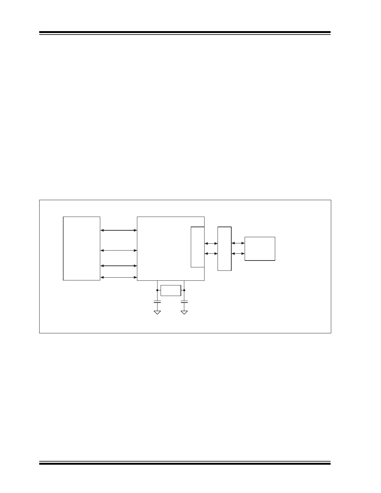
The KSZ8061MNX/MNG is a single-chip, 10BASE-T/100BASE-TX, Ethernet physical layer transceiver for transmission
and reception of data over unshielded twisted pair (UTP) cable.
The KSZ8061MNX/MNG features Quiet-Wire
®
internal filtering to reduce line emissions. It is ideal for applications, such
as automotive or industrial networks, where stringent radiated emission limits need to be met. Quiet-Wire can use low-
cost unshielded cable, where previously only shielded cable solutions were possible. The KSZ8061MNX/MNG also fea-
tures enhanced immunity to environmental EM noise.
The KSZ8061MNX/MNG offers the Media Independent Interface (MII) for direct connection with MII-compliant Ethernet
MAC processors and switches.
It is designed to exceed Automotive AEC-Q100 and EMC requirements, and features an extended temperature range
of -40°C to +105°C.
The KSZ8061MNX is supplied in a 32-lead, 5 mm × 5 mm QFN or WQFN package, while the KSZ8061MNG is in a 48-
lead, 7 mm × 7 mm QFN package.
The KSZ8061RNB and KSZ8061RND devices have an RMII interface and are described in a separate data sheet.
FIGURE 1-1:
SYSTEM BLOCK DIAGRAM
Quiet-WIRE
®
FIL
TERING
KSZ8061MN
MAGNETICS
UTP CABLE
CONNECTOR
MEDIA TYPES:
10BASE-T
100BASE-TX
10/100 Mbps
MII MAC
MII
MDC/MDIO
MANAGEMENT
XO
XI
25 MHz
XTAL
INTERRUPT
SIGNAL DETECT
2016-2017 Microchip Technology Inc.
DS00002038C-page 5
KSZ8061MNX/MNG
2.0
PIN DESCRIPTION AND CONFIGURATION
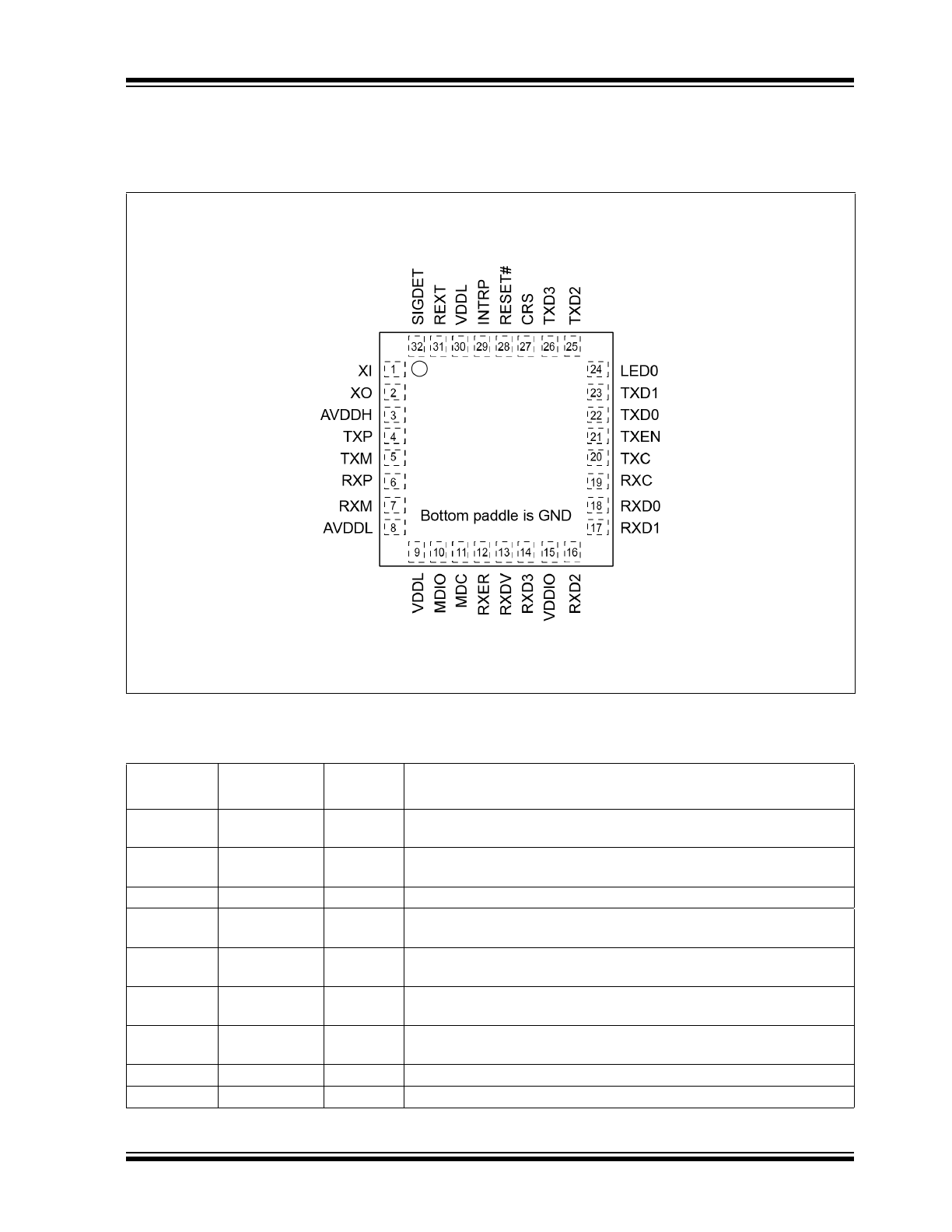
FIGURE 2-1:
32-QFN OR WQFN KSZ8061MNX PIN ASSIGNMENT (TOP VIEW)
TABLE 2-1:
SIGNALS - KSZ8061MNX (32-PIN PACKAGES)
Pin Number
Name
Type
Note 2-1
Description
1
XI
I
Crystal/Oscillator/External Clock Input
25 MHz ±50ppm. This input references the AVDDH power supply.
2
XO
O
Crystal feedback for 25-MHz crystal
This pin is a no connect if oscillator or external clock source is used.
3
AVDDH
Pwr
3.3V supply for analog TX drivers and XI/XO oscillator circuit
4
TXP
I/O
Physical transmit or receive signal (+ differential)
Transmit when in MDI mode, Receive when in MDI-X mode
5
TXM
I/O
Physical transmit or receive signal (‒ differential)
Transmit when in MDI mode, Receive when in MDI-X mode
6
RXP
I/O
Physical receive or transmit signal (+ differential)
Receive when in MDI mode, Transmit when in MDI-X mode
7
RXM
I/O
Physical receive or transmit signal (‒ differential)
Receive when in MDI mode, Transmit when in MDI-X mode
8
AVDDL
Pwr
1.2V (nominal) supply for analog core
9
VDDL
Pwr
1.2V (nominal) supply for digital core

KSZ8061MNX/MNG
DS00002038C-page 6
2016-2017 Microchip Technology Inc.
10
MDIO
Ipu/Opu
Management Interface (MIIM) Data I/O
This pin has a weak pull-up, is open-drain like, and requires an external
1.0-kΩ pull-up resistor.
11
MDC
Ipu
Management Interface (MIIM) Clock Input
This clock pin is synchronous to the MDIO data pin.
12
RXER/QWF
Ipd/O
MII Receive Error Output
Config Mode: The pull-up or pull-down value is latched as QWF at the
deassertion of reset. See
Table 2-2
for details.
13
RXDV/
CONFIG2
Ipd/O
MII Receive Data Valid Output
Config Mode: The pull-up or pull-down value is latched as CONFIG2 at
the deassertion of reset. See
Table 2-2
for details.
14
RXD3/
PHYAD0
Ipu/O
MII Receive Data Output[3] (
Note 2-2
)
Config Mode: The pull-up or pull-down value is latched as PHYADDR[0]
at the deassertion of reset. See
Table 2-2
for details.
15
VDDIO
Pwr
3.3V, 2.5V, or 1.8V supply for digital I/O
16
RXD2/
PHYAD1
Ipd/O
MII Receive Data Output[2] (
Note 2-2
)
Config Mode: The pull-up or pull-down value is latched as PHYADDR[1]
at the deassertion of reset. See
Table 2-2
for details.
17
RXD1/
PHYAD2
Ipd/O
MII Receive Data Output[1] (
Note 2-2
)
Config Mode: The pull-up or pull-down value is latched as PHYADDR[2]
at the deassertion of reset. See
Table 2-2
for details.
18
RXD0/
AUTONEG
Ipu/O
MII Receive Data Output[0] (
Note 2-2
)
Config Mode: The pull-up or pull-down value is latched as AUTONEG at
the deassertion of reset. See
Table 2-2
for details.
19
RXC/
CONFIG0
Ipd/O
MII Receive Clock Output
Config Mode: The pull-up or pull-down value is latched as CONFIG0 at
the deassertion of reset. See
Table 2-2
for details.
20
TXC
O
MII Transmit Clock Output
21
TXEN
I
MII Transmit Enable Input
22
TXD0
I
MII Transmit Data Input[0] (
Note 2-3
)
23
TXD1
I
MII Transmit Data Input[1] (
Note 2-3
)
24
LED0
O
LED0 Output
25
TXD2
I
MII Transmit Data Input[2] (
Note 2-3
)
26
TXD3
I
MII Transmit Data Input[3] (
Note 2-3
)
27
CRS/
CONFIG1
Ipd/O
MII Carrier Sense Output
Config Mode: The pull-up or pull-down value is latched as CONFIG1 at
the deassertion of reset. See
Table 2-2
for details.
28
RESET#
Ipu
Chip Reset (active low)
29
INTRP/
NAND_Tree#
Ipu/O
Programmable Interrupt Output (active low (default) or active high)
This pin has a weak pull-up, is open drain like, and requires an external
1.0-kΩ pull-up resistor.
Config Mode: The pull-up or pull-down value is latched as NAND_Tree#
at the deassertion of reset. See
Table 2-2
for details.
30
VDDL
Pwr
1.2V (nominal) supply for digital (and analog)
31
REXT
I
Set PHY transmit output current
Connect a 6.04-kΩ 1% resistor from this pin to ground.
32
SIGDET
O
Signal Detect, active high
Bottom
Paddle
GND
Gnd
Ground
TABLE 2-1:
SIGNALS - KSZ8061MNX (32-PIN PACKAGES) (CONTINUED)
Pin Number
Name
Type
Note 2-1
Description

2016-2017 Microchip Technology Inc.
DS00002038C-page 7
KSZ8061MNX/MNG
Note 2-1
Pwr = power supply
Gnd = ground
I = input
O = output
I/O = bi-directional
Ipu = Input with internal pull-up (see
Section 6.0, "Electrical Characteristics"
for value)
Ipd = Input with internal pull-down (see
Section 6.0, "Electrical Characteristics"
for value)
Ipu/O = Input with internal pull-up (see
Section 6.0, "Electrical Characteristics"
for value) during
power-up or reset; output pin otherwise.
Ipd/O = Input with internal pull-down (see
Section 6.0, "Electrical Characteristics"
for value) during
power-up or reset; output pin otherwise.
Ipu/Opu = Input and output with internal pull-up (see
Section 6.0, "Electrical Characteristics"
for value)
Note 2-2
MII Mode: The RXD[3:0] bits are synchronous with RXC. When RXDV is asserted, RXD[3:0] presents
valid data to the MAC device.
Note 2-3
MII Mode: The TXD[3:0] bits are synchronous with TXC. When TXEN is asserted, TXD[3:0] accepts
valid data from the MAC device.
KSZ8061MNX/MNG
DS00002038C-page 8
2016-2017 Microchip Technology Inc.
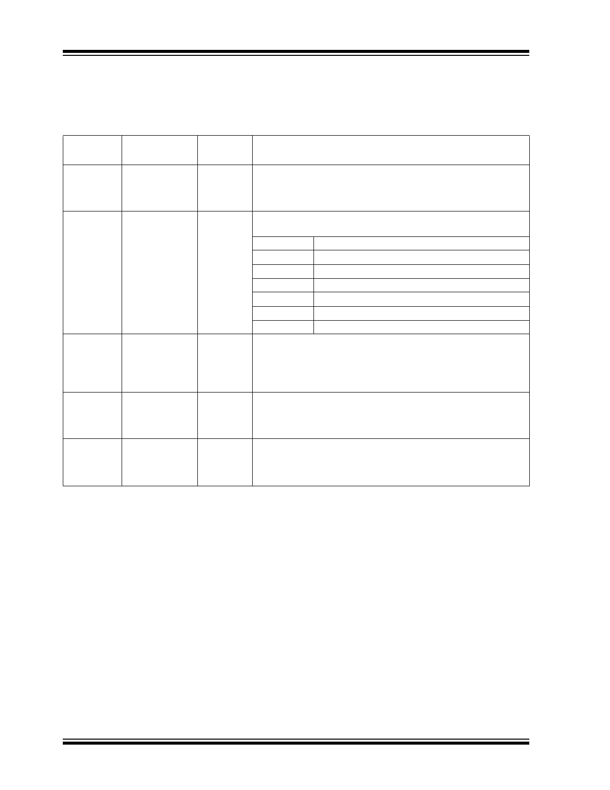
The strap-in pins are latched at the deassertion of reset. In some systems, the MAC MII receive input pins may drive
high or low during power-up or reset, and consequently cause the PHY strap-in pins on the MII signals to be latched to
the unintended high or low states. In this case, external pull-up or pull-down resistors (4.7 kΩ) should be added on these
PHY strap-in pins to ensure the intended values are strapped in correctly.
Note 2-1
Ipu/O = Input with internal pull-up (see
Section 6.0, "Electrical Characteristics"
for value) during
power-up or reset; output pin otherwise.
Ipd/O = Input with internal pull-down (see
Section 6.0, "Electrical Characteristics"
for value) during
power-up or reset; output pin otherwise.
TABLE 2-2:
STRAP-IN OPTIONS - KSZ8061MNX (32-PIN PACKAGES)
Pin Number
Pin Name
Type
Note 2-1
Description
17
16
14
RXD1/PHYAD2
RXD2/PHYAD1
RXD3/PHYAD0
Ipd/O
Ipd/O
Ipu/O
The PHY Address is latched at deassertion of reset and is configu-
rable to any value from 0 to 7.
The default PHY Address is 00001.
PHY Address bits [4:3] are set to 00 by default.
13
27
19
RXDV/CONFIG2
CRS/CONFIG1
RXC/CONFIG0
Ipd/O
Ipd/O
Ipd/O
The CONFIG[2:0] strap-in pins are latched at the deassertion of
reset.
CONFIG[2:0] Mode
000 (default) MII normal mode; Auto MDI/MDI-X disabled.
001
Reserved, not used.
010
MII normal mode; Auto MDI/MDI-X enabled.
011 - 101
Reserved, not used.
110
MII Back-to-Back; Auto MDI/MDI-X enabled.
111
Reserved, not used.
18
RXD0/
AUTONEG
Ipu/O
Auto-Negotiation Disable
Pull-up (default) = Disable Auto-Negotiation
Pull-down = Enable Auto-Negotiation
At the deassertion of reset, this pin value is inverted, and then
latched into register 0h, bit [12].
29
INTRP/
NAND_Tree#
Ipu/O
NAND Tree Mode
Pull-up (default) = Disable NAND Tree (normal operation)
Pull-down = Enable NAND Tree
At the deassertion of reset, this pin value is latched by the chip.
12
RXER/QWF
Ipd/O
Quiet-Wire
®
Filtering Disable
Pull-up = Disable Quiet-Wire Filtering
Pull-down (default) = Enable Quiet-Wire Filtering
At the deassertion of reset, this pin value is latched by the chip.
2016-2017 Microchip Technology Inc.
DS00002038C-page 9
KSZ8061MNX/MNG
FIGURE 2-2:
48-QFN KSZ8061MNG PIN ASSIGNMENT (TOP VIEW)
TABLE 2-3:
SIGNALS - KSZ8061MNG (48-PIN PACKAGE)
Pin Number
Pin Name
Type
Note 2-1
Description
1
XI
I
Crystal/Oscillator/External Clock Input
25 MHz ±50 ppm. This input references the AVDDH power supply.
2
XO
O
Crystal feedback for 25-MHz crystal
This pin is a no connect if oscillator or external clock source is used.
3
AVDDH
Pwr
3.3V supply for analog TX drivers and XI/XO oscillator circuit
4
GND
Gnd
Ground
5
TXP
I/O
Physical transmit or receive signal (+ differential)
6
TXM
I/O
Physical transmit or receive signal (‒ differential)
7
GND
Gnd
Ground
8
RXP
I/O
Physical receive or transmit signal (+ differential)
9
RXM
I/O
Physical receive or transmit signal (‒ differential)
10
GND
Gnd
Ground
11
GND
Gnd
Ground
12
AVDDL
Pwr
1.2V (nominal) supply for analog core
13
GND
Gnd
Ground
14
VDDL
Pwr
1.2V (nominal) supply for digital core
MDC
MDIO
COL
VDDL
GND
RXER
RXDV
RXD3
XI
XO
AVDDH
GND
TXP
TXM
GND
RXP
13 14 15 16 17 18 19 20
1
2
3
4
5
6
7
8
Bottom paddle is GND
RXM
GND
GND
AVDDL
9
10
11
12
GND
VDDIO
RXD2
RXD1
21 22 23 24
GND
TXD2
TXER
VDDIO
TXD1
TXD0
TXEN
TXC
36
35
34
33
32
31
30
29
GND
VDDL
RXC
RXD0
28
27
26
25
INTRP
VDDL
GND
REXT
SIGDET
GND
RESET#
VDDIO
48 47 46 45 44 43 42 41
LED1
LED0
CRS
TXD3
40 39 38 37

KSZ8061MNX/MNG
DS00002038C-page 10
2016-2017 Microchip Technology Inc.
15
COL/B-
CAST_OFF
Ipd/O
MII Collision Detect Output
Config Mode: The pull-up or pull-down value is latched as
B-CAST_OFF at the deassertion of reset. See
Table 2-4
for details.
16
MDIO
Ipu/Opu
Management Interface (MIIM) Data I/O
This pin has a weak pull-up, is open-drain like, and requires an external
1.0-kΩ pull-up resistor.
17
MDC
Ipu
Management Interface (MIIM) Clock Input
This clock pin is synchronous to the MDIO data pin.
18
RXER/QWF
Ipd/O
MII Receive Error Output
Config Mode: The pull-up or pull-down value is latched as QWF at the
deassertion of reset. See
Table 2-4
for details.
19
RXDV/
CONFIG2
Ipd/O
MII Receive Data Valid Output
Config Mode: The pull-up or pull-down value is latched as CONFIG2 at
the deassertion of reset. See
Table 2-4
for details.
20
RXD3/PHY-
AD0
Ipu/O
MII Receive Data Output[3] (
Note 2-2
)
Config Mode: The pull-up or pull-down value is latched as PHYADDR[0]
at the deassertion of reset. See
Table 2-4
for details.
21
GND
Gnd
Ground
22
VDDIO
Pwr
3.3V, 2.5V, or 1.8V supply for digital I/O
23
RXD2/PHY-
AD1
Ipd/O
MII Receive Data Output[2] (
Note 2-2
)
Config Mode: The pull-up or pull-down value is latched as PHYADDR[1]
at the deassertion of reset. See
Table 2-4
for details.
24
RXD1/PHY-
AD2
Ipd/O
MII Receive Data Output[1] (
Note 2-2
)
Config Mode: The pull-up or pull-down value is latched as PHYADDR[2]
at the deassertion of reset. See
Table 2-4
for details.
25
RXD0/
DUPLEX
Ipu/O
MII Receive Data Output[0] (
Note 2-2
)
Config Mode: The pull-up or pull-down value is latched as DUPLEX at
the deassertion of reset. See
Table 2-4
for details.
26
RXC/CONFIG0
Ipd/O
MII Receive Clock Output
Config Mode: The pull-up or pull-down value is latched as CONFIG0 at
the deassertion of reset. See
Table 2-4
for details.
27
VDDL
Pwr
1.2V (nominal) supply for digital core
28
GND
Gnd
Ground
29
TXC
O
MII Transmit Clock Output
30
TXEN
I
MII Transmit Enable Input
31
TXD0
I
MII Transmit Data Input[0] (
Note 2-3
)
32
TXD1
I
MII Transmit Data Input[1] (
Note 2-3
)
33
VDDIO
Pwr
3.3V, 2.5V, or 1.8V supply for digital I/O
34
TXER
Ipd
MII Transmit Error Input
If the MAC does not provide a TXER output signal, this pin may be
unconnected.
35
TXD2
I
MII Transmit Data Input[2] (
Note 2-3
)
36
GND
Gnd
Ground
37
TXD3
I
MII Transmit Data Input[3] (
Note 2-3
)
38
CRS/CONFIG1
Ipd/O
MII Carrier Sense Output
Config Mode: The pull-up or pull-down value is latched as CONFIG1 at
the deassertion of reset. See
Table 2-4
for details.
TABLE 2-3:
SIGNALS - KSZ8061MNG (48-PIN PACKAGE) (CONTINUED)
Pin Number
Pin Name
Type
Note 2-1
Description
2016-2017 Microchip Technology Inc.
DS00002038C-page 1
Highlights
• Single-Chip Ethernet Physical Layer Transceiver
(PHY)
• Quiet-Wire
®
technology to reduce line emissions
and enhance immunity
• Ultra-Deep Sleep standby mode
• AEC-Q100 Grade 2 Automotive
Target Applications
• Industrial control
• Vehicle on-board diagnostics (OBD)
• Automotive gateways
• Camera and sensor networking
• Infotainment
Features
• Quiet-Wire programmable EMI filter
• MII interface with MDC/MDIO management inter-
face for register configuration
• On-chip termination resistors for the differential
pairs
• LinkMD
®
+ receive signal quality indicator
• Fast start-up and link
• Ultra-Deep Sleep standby mode: CPU or signal
detect activated
• Loopback modes for diagnostics
• Programmable interrupt output
KSZ8061MNX/MNG
10BASE-T/100BASE-TX Physical Layer
Transceiver
KSZ8061MNX/MNG
DS00002038C-page 2
2016-2017 Microchip Technology Inc.
TO OUR VALUED CUSTOMERS
It is our intention to provide our valued customers with the best documentation possible to ensure successful use of your Microchip
products. To this end, we will continue to improve our publications to better suit your needs. Our publications will be refined and
enhanced as new volumes and updates are introduced.
If you have any questions or comments regarding this publication, please contact the Marketing Communications Department via
E-mail at
docerrors@microchip.com
. We welcome your feedback.
Most Current Data Sheet
To obtain the most up-to-date version of this data sheet, please register at our Worldwide Web site at:
http://www.microchip.com
You can determine the version of a data sheet by examining its literature number found on the bottom outside corner of any page.
The last character of the literature number is the version number, (e.g., DS30000000A is version A of document DS30000000).
Errata
An errata sheet, describing minor operational differences from the data sheet and recommended workarounds, may exist for cur-
rent devices. As device/documentation issues become known to us, we will publish an errata sheet. The errata will specify the
revision of silicon and revision of document to which it applies.
To determine if an errata sheet exists for a particular device, please check with one of the following:
• Microchip’s Worldwide Web site;
http://www.microchip.com
• Your local Microchip sales office (see last page)
When contacting a sales office, please specify which device, revision of silicon and data sheet (include -literature number) you are
using.
Customer Notification System
Register on our web site at
www.microchip.com
to receive the most current information on all of our products.
2016-2017 Microchip Technology Inc.
DS00002038C-page 3
KSZ8061MNX/MNG
Table of Contents
1.0 Introduction ..................................................................................................................................................................................... 4
2.0 Pin Description and Configuration .................................................................................................................................................. 5
3.0 Functional Description .................................................................................................................................................................. 13
4.0 Register Descriptions .................................................................................................................................................................... 30
5.0 Operational Characteristics ........................................................................................................................................................... 43
6.0 Electrical Characteristics ............................................................................................................................................................... 44
7.0 Timing Diagrams ........................................................................................................................................................................... 48
8.0 Reset Circuit ................................................................................................................................................................................. 55
9.0 Reference Clock — Connection and Selection ............................................................................................................................. 56
10.0 Package Outlines ........................................................................................................................................................................ 57
Appendix A: Data Sheet Revision History ........................................................................................................................................... 60
The Microchip Web Site ...................................................................................................................................................................... 61
Customer Change Notification Service ............................................................................................................................................... 61
Customer Support ............................................................................................................................................................................... 61
Product Identification System ............................................................................................................................................................. 62
KSZ8061MNX/MNG
DS00002038C-page 4
2016-2017 Microchip Technology Inc.
1.0
INTRODUCTION
1.1
General Description
The KSZ8061MNX/MNG is a single-chip, 10BASE-T/100BASE-TX, Ethernet physical layer transceiver for transmission
and reception of data over unshielded twisted pair (UTP) cable.
The KSZ8061MNX/MNG features Quiet-Wire
®
internal filtering to reduce line emissions. It is ideal for applications, such
as automotive or industrial networks, where stringent radiated emission limits need to be met. Quiet-Wire can use low-
cost unshielded cable, where previously only shielded cable solutions were possible. The KSZ8061MNX/MNG also fea-
tures enhanced immunity to environmental EM noise.
The KSZ8061MNX/MNG offers the Media Independent Interface (MII) for direct connection with MII-compliant Ethernet
MAC processors and switches.
It is designed to exceed Automotive AEC-Q100 and EMC requirements, and features an extended temperature range
of -40°C to +105°C.
The KSZ8061MNX is supplied in a 32-lead, 5 mm × 5 mm QFN or WQFN package, while the KSZ8061MNG is in a 48-
lead, 7 mm × 7 mm QFN package.
The KSZ8061RNB and KSZ8061RND devices have an RMII interface and are described in a separate data sheet.
FIGURE 1-1:
SYSTEM BLOCK DIAGRAM
Quiet-WIRE
®
FIL
TERING
KSZ8061MN
MAGNETICS
UTP CABLE
CONNECTOR
MEDIA TYPES:
10BASE-T
100BASE-TX
10/100 Mbps
MII MAC
MII
MDC/MDIO
MANAGEMENT
XO
XI
25 MHz
XTAL
INTERRUPT
SIGNAL DETECT
2016-2017 Microchip Technology Inc.
DS00002038C-page 5
KSZ8061MNX/MNG
2.0
PIN DESCRIPTION AND CONFIGURATION
FIGURE 2-1:
32-QFN OR WQFN KSZ8061MNX PIN ASSIGNMENT (TOP VIEW)
TABLE 2-1:
SIGNALS - KSZ8061MNX (32-PIN PACKAGES)
Pin Number
Name
Type
Note 2-1
Description
1
XI
I
Crystal/Oscillator/External Clock Input
25 MHz ±50ppm. This input references the AVDDH power supply.
2
XO
O
Crystal feedback for 25-MHz crystal
This pin is a no connect if oscillator or external clock source is used.
3
AVDDH
Pwr
3.3V supply for analog TX drivers and XI/XO oscillator circuit
4
TXP
I/O
Physical transmit or receive signal (+ differential)
Transmit when in MDI mode, Receive when in MDI-X mode
5
TXM
I/O
Physical transmit or receive signal (‒ differential)
Transmit when in MDI mode, Receive when in MDI-X mode
6
RXP
I/O
Physical receive or transmit signal (+ differential)
Receive when in MDI mode, Transmit when in MDI-X mode
7
RXM
I/O
Physical receive or transmit signal (‒ differential)
Receive when in MDI mode, Transmit when in MDI-X mode
8
AVDDL
Pwr
1.2V (nominal) supply for analog core
9
VDDL
Pwr
1.2V (nominal) supply for digital core
KSZ8061MNX/MNG
DS00002038C-page 6
2016-2017 Microchip Technology Inc.
10
MDIO
Ipu/Opu
Management Interface (MIIM) Data I/O
This pin has a weak pull-up, is open-drain like, and requires an external
1.0-kΩ pull-up resistor.
11
MDC
Ipu
Management Interface (MIIM) Clock Input
This clock pin is synchronous to the MDIO data pin.
12
RXER/QWF
Ipd/O
MII Receive Error Output
Config Mode: The pull-up or pull-down value is latched as QWF at the
deassertion of reset. See
Table 2-2
for details.
13
RXDV/
CONFIG2
Ipd/O
MII Receive Data Valid Output
Config Mode: The pull-up or pull-down value is latched as CONFIG2 at
the deassertion of reset. See
Table 2-2
for details.
14
RXD3/
PHYAD0
Ipu/O
MII Receive Data Output[3] (
Note 2-2
)
Config Mode: The pull-up or pull-down value is latched as PHYADDR[0]
at the deassertion of reset. See
Table 2-2
for details.
15
VDDIO
Pwr
3.3V, 2.5V, or 1.8V supply for digital I/O
16
RXD2/
PHYAD1
Ipd/O
MII Receive Data Output[2] (
Note 2-2
)
Config Mode: The pull-up or pull-down value is latched as PHYADDR[1]
at the deassertion of reset. See
Table 2-2
for details.
17
RXD1/
PHYAD2
Ipd/O
MII Receive Data Output[1] (
Note 2-2
)
Config Mode: The pull-up or pull-down value is latched as PHYADDR[2]
at the deassertion of reset. See
Table 2-2
for details.
18
RXD0/
AUTONEG
Ipu/O
MII Receive Data Output[0] (
Note 2-2
)
Config Mode: The pull-up or pull-down value is latched as AUTONEG at
the deassertion of reset. See
Table 2-2
for details.
19
RXC/
CONFIG0
Ipd/O
MII Receive Clock Output
Config Mode: The pull-up or pull-down value is latched as CONFIG0 at
the deassertion of reset. See
Table 2-2
for details.
20
TXC
O
MII Transmit Clock Output
21
TXEN
I
MII Transmit Enable Input
22
TXD0
I
MII Transmit Data Input[0] (
Note 2-3
)
23
TXD1
I
MII Transmit Data Input[1] (
Note 2-3
)
24
LED0
O
LED0 Output
25
TXD2
I
MII Transmit Data Input[2] (
Note 2-3
)
26
TXD3
I
MII Transmit Data Input[3] (
Note 2-3
)
27
CRS/
CONFIG1
Ipd/O
MII Carrier Sense Output
Config Mode: The pull-up or pull-down value is latched as CONFIG1 at
the deassertion of reset. See
Table 2-2
for details.
28
RESET#
Ipu
Chip Reset (active low)
29
INTRP/
NAND_Tree#
Ipu/O
Programmable Interrupt Output (active low (default) or active high)
This pin has a weak pull-up, is open drain like, and requires an external
1.0-kΩ pull-up resistor.
Config Mode: The pull-up or pull-down value is latched as NAND_Tree#
at the deassertion of reset. See
Table 2-2
for details.
30
VDDL
Pwr
1.2V (nominal) supply for digital (and analog)
31
REXT
I
Set PHY transmit output current
Connect a 6.04-kΩ 1% resistor from this pin to ground.
32
SIGDET
O
Signal Detect, active high
Bottom
Paddle
GND
Gnd
Ground
TABLE 2-1:
SIGNALS - KSZ8061MNX (32-PIN PACKAGES) (CONTINUED)
Pin Number
Name
Type
Note 2-1
Description
2016-2017 Microchip Technology Inc.
DS00002038C-page 7
KSZ8061MNX/MNG
Note 2-1
Pwr = power supply
Gnd = ground
I = input
O = output
I/O = bi-directional
Ipu = Input with internal pull-up (see
Section 6.0, "Electrical Characteristics"
for value)
Ipd = Input with internal pull-down (see
Section 6.0, "Electrical Characteristics"
for value)
Ipu/O = Input with internal pull-up (see
Section 6.0, "Electrical Characteristics"
for value) during
power-up or reset; output pin otherwise.
Ipd/O = Input with internal pull-down (see
Section 6.0, "Electrical Characteristics"
for value) during
power-up or reset; output pin otherwise.
Ipu/Opu = Input and output with internal pull-up (see
Section 6.0, "Electrical Characteristics"
for value)
Note 2-2
MII Mode: The RXD[3:0] bits are synchronous with RXC. When RXDV is asserted, RXD[3:0] presents
valid data to the MAC device.
Note 2-3
MII Mode: The TXD[3:0] bits are synchronous with TXC. When TXEN is asserted, TXD[3:0] accepts
valid data from the MAC device.
KSZ8061MNX/MNG
DS00002038C-page 8
2016-2017 Microchip Technology Inc.
The strap-in pins are latched at the deassertion of reset. In some systems, the MAC MII receive input pins may drive
high or low during power-up or reset, and consequently cause the PHY strap-in pins on the MII signals to be latched to
the unintended high or low states. In this case, external pull-up or pull-down resistors (4.7 kΩ) should be added on these
PHY strap-in pins to ensure the intended values are strapped in correctly.
Note 2-1
Ipu/O = Input with internal pull-up (see
Section 6.0, "Electrical Characteristics"
for value) during
power-up or reset; output pin otherwise.
Ipd/O = Input with internal pull-down (see
Section 6.0, "Electrical Characteristics"
for value) during
power-up or reset; output pin otherwise.
TABLE 2-2:
STRAP-IN OPTIONS - KSZ8061MNX (32-PIN PACKAGES)
Pin Number
Pin Name
Type
Note 2-1
Description
17
16
14
RXD1/PHYAD2
RXD2/PHYAD1
RXD3/PHYAD0
Ipd/O
Ipd/O
Ipu/O
The PHY Address is latched at deassertion of reset and is configu-
rable to any value from 0 to 7.
The default PHY Address is 00001.
PHY Address bits [4:3] are set to 00 by default.
13
27
19
RXDV/CONFIG2
CRS/CONFIG1
RXC/CONFIG0
Ipd/O
Ipd/O
Ipd/O
The CONFIG[2:0] strap-in pins are latched at the deassertion of
reset.
CONFIG[2:0] Mode
000 (default) MII normal mode; Auto MDI/MDI-X disabled.
001
Reserved, not used.
010
MII normal mode; Auto MDI/MDI-X enabled.
011 - 101
Reserved, not used.
110
MII Back-to-Back; Auto MDI/MDI-X enabled.
111
Reserved, not used.
18
RXD0/
AUTONEG
Ipu/O
Auto-Negotiation Disable
Pull-up (default) = Disable Auto-Negotiation
Pull-down = Enable Auto-Negotiation
At the deassertion of reset, this pin value is inverted, and then
latched into register 0h, bit [12].
29
INTRP/
NAND_Tree#
Ipu/O
NAND Tree Mode
Pull-up (default) = Disable NAND Tree (normal operation)
Pull-down = Enable NAND Tree
At the deassertion of reset, this pin value is latched by the chip.
12
RXER/QWF
Ipd/O
Quiet-Wire
®
Filtering Disable
Pull-up = Disable Quiet-Wire Filtering
Pull-down (default) = Enable Quiet-Wire Filtering
At the deassertion of reset, this pin value is latched by the chip.
2016-2017 Microchip Technology Inc.
DS00002038C-page 9
KSZ8061MNX/MNG
FIGURE 2-2:
48-QFN KSZ8061MNG PIN ASSIGNMENT (TOP VIEW)
TABLE 2-3:
SIGNALS - KSZ8061MNG (48-PIN PACKAGE)
Pin Number
Pin Name
Type
Note 2-1
Description
1
XI
I
Crystal/Oscillator/External Clock Input
25 MHz ±50 ppm. This input references the AVDDH power supply.
2
XO
O
Crystal feedback for 25-MHz crystal
This pin is a no connect if oscillator or external clock source is used.
3
AVDDH
Pwr
3.3V supply for analog TX drivers and XI/XO oscillator circuit
4
GND
Gnd
Ground
5
TXP
I/O
Physical transmit or receive signal (+ differential)
6
TXM
I/O
Physical transmit or receive signal (‒ differential)
7
GND
Gnd
Ground
8
RXP
I/O
Physical receive or transmit signal (+ differential)
9
RXM
I/O
Physical receive or transmit signal (‒ differential)
10
GND
Gnd
Ground
11
GND
Gnd
Ground
12
AVDDL
Pwr
1.2V (nominal) supply for analog core
13
GND
Gnd
Ground
14
VDDL
Pwr
1.2V (nominal) supply for digital core
MDC
MDIO
COL
VDDL
GND
RXER
RXDV
RXD3
XI
XO
AVDDH
GND
TXP
TXM
GND
RXP
13 14 15 16 17 18 19 20
1
2
3
4
5
6
7
8
Bottom paddle is GND
RXM
GND
GND
AVDDL
9
10
11
12
GND
VDDIO
RXD2
RXD1
21 22 23 24
GND
TXD2
TXER
VDDIO
TXD1
TXD0
TXEN
TXC
36
35
34
33
32
31
30
29
GND
VDDL
RXC
RXD0
28
27
26
25
INTRP
VDDL
GND
REXT
SIGDET
GND
RESET#
VDDIO
48 47 46 45 44 43 42 41
LED1
LED0
CRS
TXD3
40 39 38 37
KSZ8061MNX/MNG
DS00002038C-page 10
2016-2017 Microchip Technology Inc.
15
COL/B-
CAST_OFF
Ipd/O
MII Collision Detect Output
Config Mode: The pull-up or pull-down value is latched as
B-CAST_OFF at the deassertion of reset. See
Table 2-4
for details.
16
MDIO
Ipu/Opu
Management Interface (MIIM) Data I/O
This pin has a weak pull-up, is open-drain like, and requires an external
1.0-kΩ pull-up resistor.
17
MDC
Ipu
Management Interface (MIIM) Clock Input
This clock pin is synchronous to the MDIO data pin.
18
RXER/QWF
Ipd/O
MII Receive Error Output
Config Mode: The pull-up or pull-down value is latched as QWF at the
deassertion of reset. See
Table 2-4
for details.
19
RXDV/
CONFIG2
Ipd/O
MII Receive Data Valid Output
Config Mode: The pull-up or pull-down value is latched as CONFIG2 at
the deassertion of reset. See
Table 2-4
for details.
20
RXD3/PHY-
AD0
Ipu/O
MII Receive Data Output[3] (
Note 2-2
)
Config Mode: The pull-up or pull-down value is latched as PHYADDR[0]
at the deassertion of reset. See
Table 2-4
for details.
21
GND
Gnd
Ground
22
VDDIO
Pwr
3.3V, 2.5V, or 1.8V supply for digital I/O
23
RXD2/PHY-
AD1
Ipd/O
MII Receive Data Output[2] (
Note 2-2
)
Config Mode: The pull-up or pull-down value is latched as PHYADDR[1]
at the deassertion of reset. See
Table 2-4
for details.
24
RXD1/PHY-
AD2
Ipd/O
MII Receive Data Output[1] (
Note 2-2
)
Config Mode: The pull-up or pull-down value is latched as PHYADDR[2]
at the deassertion of reset. See
Table 2-4
for details.
25
RXD0/
DUPLEX
Ipu/O
MII Receive Data Output[0] (
Note 2-2
)
Config Mode: The pull-up or pull-down value is latched as DUPLEX at
the deassertion of reset. See
Table 2-4
for details.
26
RXC/CONFIG0
Ipd/O
MII Receive Clock Output
Config Mode: The pull-up or pull-down value is latched as CONFIG0 at
the deassertion of reset. See
Table 2-4
for details.
27
VDDL
Pwr
1.2V (nominal) supply for digital core
28
GND
Gnd
Ground
29
TXC
O
MII Transmit Clock Output
30
TXEN
I
MII Transmit Enable Input
31
TXD0
I
MII Transmit Data Input[0] (
Note 2-3
)
32
TXD1
I
MII Transmit Data Input[1] (
Note 2-3
)
33
VDDIO
Pwr
3.3V, 2.5V, or 1.8V supply for digital I/O
34
TXER
Ipd
MII Transmit Error Input
If the MAC does not provide a TXER output signal, this pin may be
unconnected.
35
TXD2
I
MII Transmit Data Input[2] (
Note 2-3
)
36
GND
Gnd
Ground
37
TXD3
I
MII Transmit Data Input[3] (
Note 2-3
)
38
CRS/CONFIG1
Ipd/O
MII Carrier Sense Output
Config Mode: The pull-up or pull-down value is latched as CONFIG1 at
the deassertion of reset. See
Table 2-4
for details.
TABLE 2-3:
SIGNALS - KSZ8061MNG (48-PIN PACKAGE) (CONTINUED)
Pin Number
Pin Name
Type
Note 2-1
Description