

DS00002245B-page 1
2017 Microchip Technology Inc.
Highlights
• Single-Chip Ethernet Physical Layer Transceiver
(PHY)
• HP Auto-MDIX Support
Target Applications
• Printer
• LOM
• Game Console
• IPTV
• IP Phone
• IP Set-Top Box
Key Benefits
• Single-Chip 10BASE-T/100BASE-TX Physical
Layer Solution
• Fully Compliant To IEEE 802.3u Standard
• Low Power CMOS Design, Power Consumption
of <180 mW
• HP Auto MDI/MDI-X For Reliable Detection and
Correction for Straight-Through and Crossover
Cables with Disable and Enable Option
• Robust Operation Over Standard Cables
• Power Down and Power Saving Modes
• MII Interface Support (KSZ8041NL Only)
• RMII Interface Support with External 50-MHz
System Clock (KSZ8041NL Only)
• RMII Interface Support with 25-MHz Crystal/Clock
Input and 50-MHz Reference Clock Output to
MAC (KSZ8041RNL Only)
• MIIM (MDC/MDIO) Management Bus to 6.25 MHz
for Rapid PHY Register Configuration
• Interrupt Pin Option
• Programmable LED Outputs for Link, Activity
and Speed
• ESD Rating (6 kV)
• Single Power Supply (3.3V)
• Built-in 1.8V Regulator for Core
• Available In 32-pin 5 mm × 5 mm QFN Package
KSZ8041NL/RNL
10BASE-T/100BASE-TX
Physical Layer Transceiver

KSZ8041NL/RNL
DS00002245B-page 2
2017 Microchip Technology Inc.
TO OUR VALUED CUSTOMERS
It is our intention to provide our valued customers with the best documentation possible to ensure successful use of your Microchip
products. To this end, we will continue to improve our publications to better suit your needs. Our publications will be refined and
enhanced as new volumes and updates are introduced.
If you have any questions or comments regarding this publication, please contact the Marketing Communications Department via
E-mail at
docerrors@microchip.com
. We welcome your feedback.
Most Current Data Sheet
To obtain the most up-to-date version of this data sheet, please register at our Worldwide Web site at:
http://www.microchip.com
You can determine the version of a data sheet by examining its literature number found on the bottom outside corner of any page.
The last character of the literature number is the version number, (e.g., DS30000000A is version A of document DS30000000).
Errata
An errata sheet, describing minor operational differences from the data sheet and recommended workarounds, may exist for cur-
rent devices. As device/documentation issues become known to us, we will publish an errata sheet. The errata will specify the
revision of silicon and revision of document to which it applies.
To determine if an errata sheet exists for a particular device, please check with one of the following:
• Microchip’s Worldwide Web site;
http://www.microchip.com
• Your local Microchip sales office (see last page)
When contacting a sales office, please specify which device, revision of silicon and data sheet (include -literature number) you are
using.
Customer Notification System
Register on our web site at
www.microchip.com
to receive the most current information on all of our products.

2017 Microchip Technology Inc.
DS00002245B-page 3
KSZ8041NL/RNL
Table of Contents
1.0 General Description ........................................................................................................................................................................ 4
2.0 Pin Description and Configuration .................................................................................................................................................. 6
3.0 Functional Description .................................................................................................................................................................. 17
4.0 Registers ....................................................................................................................................................................................... 29
5.0 Operational Characteristics ........................................................................................................................................................... 38
6.0 Electrical Characteristics ............................................................................................................................................................... 39
7.0 Timing Diagrams ........................................................................................................................................................................... 40
8.0 Selection of Isolation Transformer ................................................................................................................................................ 50
9.0 Selection of Reference Crystal ..................................................................................................................................................... 51
10.0 Package Outline & Recommended Land Pattern ....................................................................................................................... 52
Appendix A: Data Sheet Revision History ........................................................................................................................................... 53
The Microchip Web Site ...................................................................................................................................................................... 54
Customer Change Notification Service ............................................................................................................................................... 54
Customer Support ............................................................................................................................................................................... 54
Product Identification System ............................................................................................................................................................. 55
KSZ8041NL/RNL
DS0002245B-page 4
2017 Microchip Technology Inc.
1.0
GENERAL DESCRIPTION
The KSZ8041NL is a single supply 10BASE-T/100BASE-TX physical layer transceiver, which provides
MII/RMII interfaces to transmit and receive data. A unique mixed-signal design extends signaling distance
while reducing power consumption.
HP Auto MDI/MDI-X provides the most robust solution for eliminating the need to differentiate between
crossover and straight-through cables.
The KSZ8041NL represents a new level of features and performance and is an ideal choice of physical layer
transceiver for 10BASE-T/100BASE-TX applications.
The KSZ8041RNL is an enhanced Reduced Media Independent Interface (RMII) version of the
KSZ8041NL that does not require a 50-MHz system clock. It uses a 25-MHz crystal for its input reference
clock and outputs a 50-MHz RMII reference clock to the media access control (MAC).
The KSZ8041NL and KSZ8041RNL are available in 32-pin, lead-free QFN packages (see
Product Identifi-
cation System
).
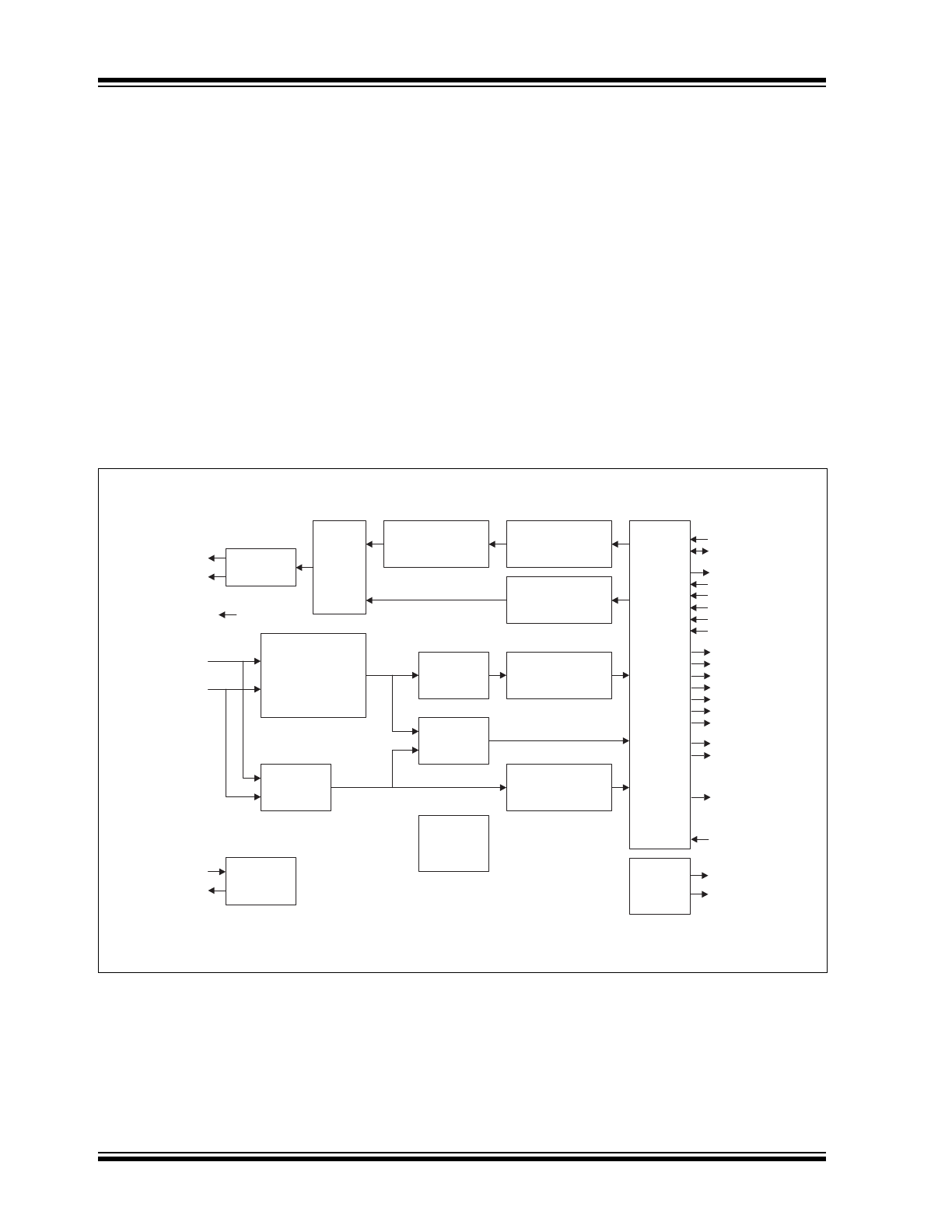
FIGURE 1-1:
KSZ8041NL FUNCTIONAL DIAGRAM
10/100
Pulse
Shaper
NRZ/NRZI
MLT3 Encoder
Parallel /Serial
Manchester Encoder
4B/5B Encoder
Scrambler
Parallel /Serial
Transmitter
TX+
TX-
Adaptive EQ
Base Line
Wander Correction
MLT3 Decoder
NRZI/NRZ
Clock
Recovery
4B/5B Decoder
Descrambler
Serial/Parallel
Auto
Negotiation
10Base-T
Receiver
Manchester Decoder
Serial/Parallel
PLL
LED
Driver
MII/RMII
Registers
and
Controller
Interface
RX-
RX+
XI
XO
LED1
LED0
Power Down
Power Saving
TXD3
TXD0
TXD1
TXD2
RXD3
TXEN
TXC
MDC
MDIO
RXER
RXD0
RXD1
RXD2
REXT
RXC
RXDV
CRS
COL
RST#
INTRP
2017 Microchip Technology Inc.
DS0002245B-page 5
KSZ8041NL/RNL
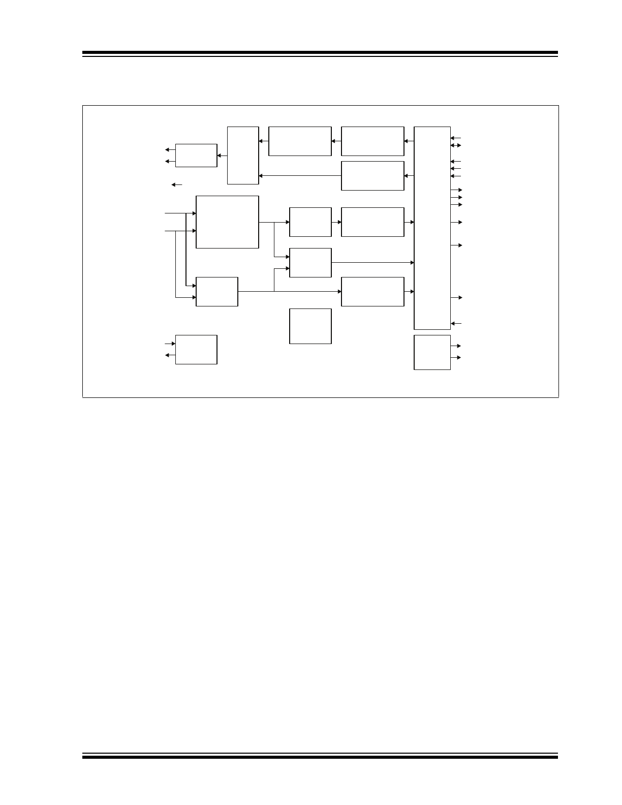
FIGURE 1-2:
KSZ8041RNL FUNCTIONAL DIAGRAM
10/100
Pulse
Shaper
NRZ/NRZI
MLT3 Encoder
Parallel/Serial
Manchester Encoder
4B/5B Encoder
Scrambler
Parallel/Serial
Transmitter
TX+
TX-
Adaptive EQ
Base Line
Wander Correction
MLT3 Decoder
NRZI/NRZ
Clock
Recovery
4B/5B Decoder
Descrambler
Serial/Parallel
Auto
Negotiation
10Base-T
Receiver
Manchester Decoder
Serial/Parallel
PLL
LED
Driver
RMII
RX-
RX+
XI
XO
LED1
LED0
Power Down
Power Saving
TXD1
TXD0
RXD1
TX_EN
MDC
MDIO
RX_ER
RXD0
REXT
REF_CLK
CRS_DV
RST#
INTRP
KSZ8041NL/RNL
DS00002245B-page 6
2017 Microchip Technology Inc.
2.0
PIN DESCRIPTION AND CONFIGURATION
2.1
KSZ8041NL Pin Description and Configuration
FIGURE 2-1:
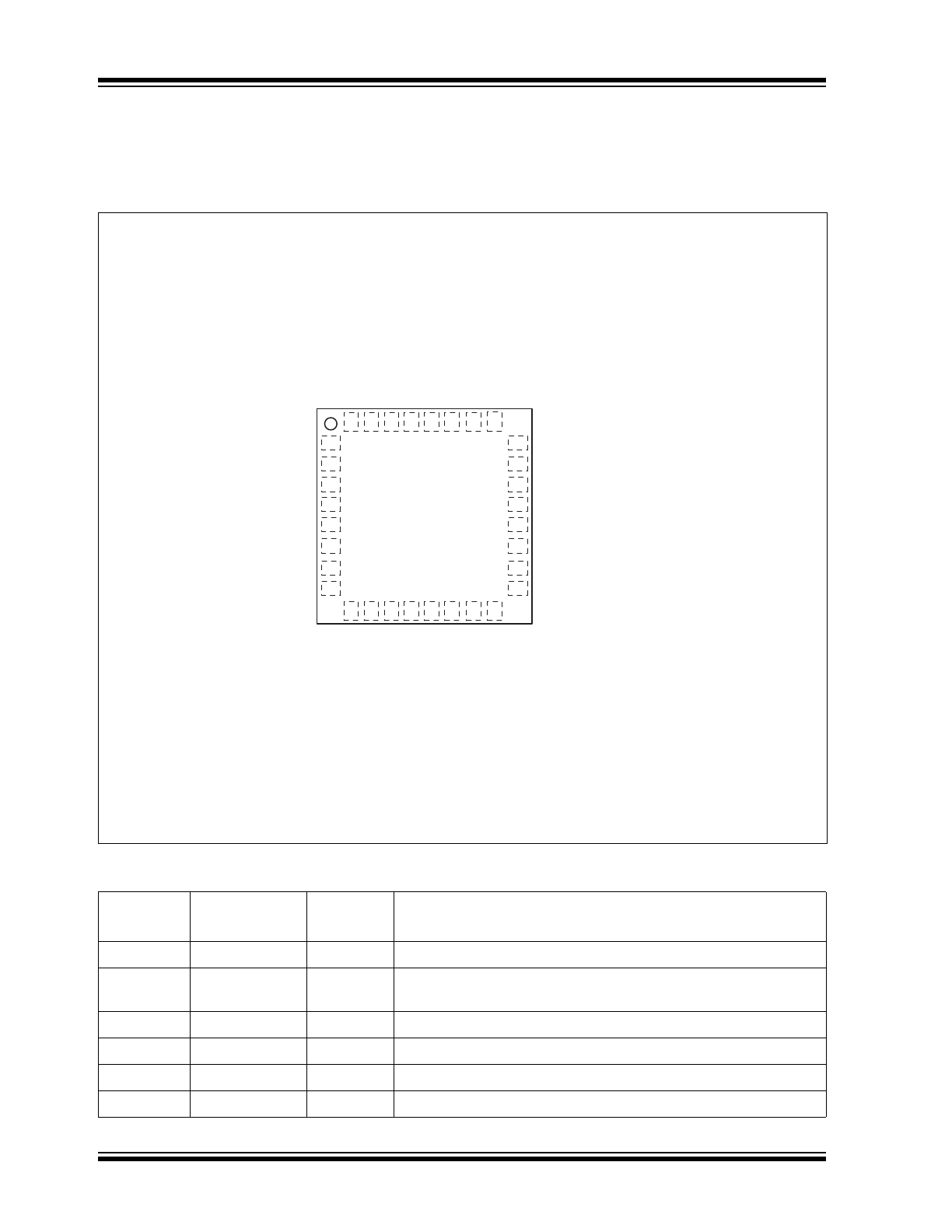
KSZ8041NL 32-QFN PIN ASSIGNMENT (TOP VIEW)
TABLE 2-1:
KSZ8041NL PIN DESCRIPTION
Pin Number
Symbol
Buffer Type
(
Note 2-1
)
Description
1
GND
Gnd
Ground
2
VDDPLL_1.8
P
1.8V Analog V
DD
Decouple with 1.0-µF and 0.1-µF capacitors to ground.
3
VDDA_3.3
P
3.3V Analog V
DD
4
RX-
I/O
Physical receive or transmit signal (- differential)
5
RX+
I/O
Physical receive or transmit signal (+ differential)
6
TX-
I/O
Physical transmit or receive signal (- differential)
GND
VDDPLL_1.8
VDDA_3.3
RX-
RX+
TX-
TX+
XO
RXD3/PHY
A
D0
MDC
MDIO
REXT
XI/REFCLK
RXD2/PHY
A
D1
RXD1/RXD[1]/PHY
AD2
RXD0/RXD[0]/DUPLEX
1
2
3
4
5
6
7
8
9
10
11 12 13 14
15
16
24
23
22
21
20
19
18
17
32 31 30 29 28 27
26
25
TXD0/TXD[0]
TXEN/TX_EN
TXC
INTRP
RXER/RX_ER/ISO
RXC
RXDV/CRSDV/CONFIG2
VDDIO_3.3
COL/CONFIG0
CRS/CONFIG1
LED0/NW
A
YEN
LED1/SPEED
RST#
TXD3
TXD2
TXD1/TXD[1]
Paddle Ground
on bottom of chip

2017 Microchip Technology Inc.
DS00002245B-page 7
KSZ8041NL/RNL
7
TX+
I/O
Physical transmit or receive signal (+ differential)
8
XO
O
Crystal Feedback.
This pin is used only in MII mode when a 25-MHz crystal is used.
This pin is a no connect if an oscillator or an external clock source is
used, or if RMII mode is selected.
9
XI /
REFCLK
I
Crystal/Oscillator/External Clock Input:
MII mode: 25 MHz ±50 ppm (crystal, oscillator, or external clock)
RMII mode: 50 MHz ±50 ppm (oscillator or external clock only)
10
REXT
I/O
Set physical transmit output current.
Connect a 6.49-K
resistor in parallel with a 100-pF capacitor to
ground on this pin.
11
MDIO
I/O
Management Interface (MII) Data I/O
This pin requires an external 4.7-K
pull-up resistor.
12
MDC
I
Management Interface (MII) Clock Input
This pin is synchronous to the MDIO data interface.
13
RXD3 /
PHYAD0
Ipu/O
MII mode: Receive Data Output[3] (
Note 2-2
)
Config mode: The pull-up/pull-down value is latched as PHY-
ADDR[0] during power-up or reset. See “
Strap-In option –
KSZ8041NL
” for details.
14
RXD2 /
PHYAD1
Ipd/O
MII mode: Receive Data Output[2] (
Note 2-2
)
Config mode: The pull-up/pull-down value is latched as PHY-
ADDR[1] during power-up or reset. See “
Strap-In option –
KSZ8041NL
” for details.
15
RXD1 /
RXD[1] /
PHYAD2
Ipd/O
MII mode: Receive Data Output[1] (
Note 2-2
)
RMII mode: Receive Data Output[1] (
Note 2-3
)
Config mode: The pull-up/pull-down value is latched as PHY-
ADDR[2] during power-up or reset. See “
Strap-In option –
KSZ8041NL
” for details.
16
RXD0 /
RXD[0] /
DUPLEX
Ipu/O
MII mode: Receive Data Output[0] (
Note 2-2
).
RMII mode: Receive Data Output[0] (
Note 2-3
).
Config mode: Latched as DUPLEX (register 0h, bit 8) during power-
up or reset. See “
Strap-In option – KSZ8041NL
” for details.
17
VDDIO_3.3
P
3.3V Digital V
DD
18
RXDV /
CRSDV /
CONFIG2
Ipd/O
MII mode: Receive Data Valid Output
RMII mode: Carrier Sense/Receive Data Valid Output
Config mode: The pull-up/pull-down value is latched as CONFIG2
during power-up or reset. See “
Strap-In option – KSZ8041NL
”
for details.
19
RXC
O
MII mode: Receive Clock Output
20
RXER /
RX_ER /
ISO
Ipd/O
MII mode: Receive Error Output
RMII mode: Receive Error Output
Config mode: The pull-up/pull-down value is latched as ISOLATE
during power-up or reset. See “
Strap-In option – KSZ8041NL
” for
details.
TABLE 2-1:
KSZ8041NL PIN DESCRIPTION (CONTINUED)
Pin Number
Symbol
Buffer Type
(
Note 2-1
)
Description

KSZ8041NL/RNL
DS00002245B-page 8
2017 Microchip Technology Inc.
21
INTRP
Opu
Interrupt Output: Programmable Interrupt Output
Register 1Bh is the Interrupt Control/Status Register for program-
ming the interrupt conditions and reading the interrupt status. Regis-
ter 1Fh bit 9 sets the interrupt output to active low (default) or active
high.
22
TXC
O
MII mode: Transmit Clock Output
23
TXEN /
TX_EN
I
MII mode: Transmit Enable Input
RMII mode: Transmit Enable Input
24
TXD0 /
TXD[0]
I
MII mode: Transmit Data Input[0]
(
Note 2-4
)
RMII mode: Transmit Data Input[0]
(
Note 2-5
)
25
TXD1 /
TXD[1]
I
MII mode: Transmit Data Input[1]
(
Note 2-4
)
RMII mode: Transmit Data Input[1]
(
Note 2-5
)
26
TXD2
I
MII mode: Transmit Data Input[2]
(
Note 2-4
)
27
TXD3
I
MII mode: Transmit Data Input[3]
(
Note 2-4
)
28
COL/CONFIG0
Ipd/O
MII mode: Collision Detect Output
Config mode: The pull-up/pull-down value is latched as CONFIG0
during power-up or reset. See “
Strap-In option – KSZ8041NL
” for
details.
29
CRS/CONFIG1
Ipd/O
MII mode: Collision Sense Output
Config mode: The pull-up/pull-down value is latched as CONFIG1
during power-up or reset. See “
Strap-In option – KSZ8041NL
” for
details.
TABLE 2-1:
KSZ8041NL PIN DESCRIPTION (CONTINUED)
Pin Number
Symbol
Buffer Type
(
Note 2-1
)
Description
2017 Microchip Technology Inc.
DS00002245B-page 9
KSZ8041NL/RNL
30
LED0 / NWAYEN
Ipu/O
LED Output: Programmable LED0 Output
Config ode: Latched as Auto-Negotiation Enable (register 0h, bit 12)
during power-up or reset. See
Strap-In option – KSZ8041NL
for
details.
The LED0 pin is programmable via register 1Eh bits [15:14] and is
defined as follows:
LED Mode = [00]
LED Mode = [01]
LED Mode = [10]
Reserved
LED Mode = [11]
Reserved
TABLE 2-1:
KSZ8041NL PIN DESCRIPTION (CONTINUED)
Pin Number
Symbol
Buffer Type
(
Note 2-1
)
Description
Link/Activity
Pin State
LED Definition
No Link
H
OFF
Link
L
ON
Activity
Toggle
Blinking
Link/Activity
Pin State
LED Definition
No Link
H
OFF
Link
L
ON
KSZ8041NL/RNL
DS00002245B-page 10
2017 Microchip Technology Inc.
Note 2-1
P = Power supply
Gnd = Ground
I = Input
O = Output
I/O = Bi-directional
Ipd = Input with internal pull-down (40K ±30%)
Ipu = Input with internal pull-up (40K ±30%)
Opu = Output with internal pull-up (40K ±30%)
Ipu/O = Input with internal pull-up (40K ±30%) during power-up/reset; output pin otherwise.
Ipd/O = Input with internal pull-down (40K ±30%) during power-up/reset; output pin otherwise.
Note 2-2
MII Rx mode: The RXD[3:0] bits are synchronous with RXCLK. When RXDV is asserted, RXD[3:0]
presents a valid data to the MAC through the MII. RXD[3:0] is invalid when RXDV is deasserted.
Note 2-3
RMII Rx mode: The RXD[1:0] bits are synchronous with REF_CLK. For each clock period in which
CRS_DV is asserted, two bits of recovered data are sent from the PHY.
Note 2-4
MII Tx mode: The TXD[3:0] bits are synchronous with TXCLK. When TXEN is asserted, TXD[3:0]
presents a valid data from the MAC through the MII. TXD[3..0] has no effect when TXEN is
deasserted.
Note 2-5
RMII Tx mode: The TXD[1:0] bits are synchronous with REF_CLK. For each clock period in which
TX_EN is asserted, two bits of data are received by the PHY from the MAC.
31
LED1 / SPEED
Ipu/O
LED Output: Programmable LED1 Output
Config mode: Latched as SPEED (register 0h, bit 13) during power-
up or reset. See
Strap-In option – KSZ8041NL
for details.
The LED1 pin is programmable via register 1Eh bits [15:14] and is
defined as follows:
LED Mode = [00]
LED Mode = [01]
LED Mode = [10]
Reserved
LED Mode = [11]
Reserved
32
RST#
I
Chip Reset (active low)
PADDLE
GND
Gnd
Ground
TABLE 2-1:
KSZ8041NL PIN DESCRIPTION (CONTINUED)
Pin Number
Symbol
Buffer Type
(
Note 2-1
)
Description
Speed
Pin State
LED Definition
10BT
H
OFF
100BT
L
ON
Activity
Pin State
LED Definition
No Activity
H
OFF
Activity
Toggle
Blinking
DS00002245B-page 1
2017 Microchip Technology Inc.
Highlights
• Single-Chip Ethernet Physical Layer Transceiver
(PHY)
• HP Auto-MDIX Support
Target Applications
• Printer
• LOM
• Game Console
• IPTV
• IP Phone
• IP Set-Top Box
Key Benefits
• Single-Chip 10BASE-T/100BASE-TX Physical
Layer Solution
• Fully Compliant To IEEE 802.3u Standard
• Low Power CMOS Design, Power Consumption
of <180 mW
• HP Auto MDI/MDI-X For Reliable Detection and
Correction for Straight-Through and Crossover
Cables with Disable and Enable Option
• Robust Operation Over Standard Cables
• Power Down and Power Saving Modes
• MII Interface Support (KSZ8041NL Only)
• RMII Interface Support with External 50-MHz
System Clock (KSZ8041NL Only)
• RMII Interface Support with 25-MHz Crystal/Clock
Input and 50-MHz Reference Clock Output to
MAC (KSZ8041RNL Only)
• MIIM (MDC/MDIO) Management Bus to 6.25 MHz
for Rapid PHY Register Configuration
• Interrupt Pin Option
• Programmable LED Outputs for Link, Activity
and Speed
• ESD Rating (6 kV)
• Single Power Supply (3.3V)
• Built-in 1.8V Regulator for Core
• Available In 32-pin 5 mm × 5 mm QFN Package
KSZ8041NL/RNL
10BASE-T/100BASE-TX
Physical Layer Transceiver
KSZ8041NL/RNL
DS00002245B-page 2
2017 Microchip Technology Inc.
TO OUR VALUED CUSTOMERS
It is our intention to provide our valued customers with the best documentation possible to ensure successful use of your Microchip
products. To this end, we will continue to improve our publications to better suit your needs. Our publications will be refined and
enhanced as new volumes and updates are introduced.
If you have any questions or comments regarding this publication, please contact the Marketing Communications Department via
E-mail at
docerrors@microchip.com
. We welcome your feedback.
Most Current Data Sheet
To obtain the most up-to-date version of this data sheet, please register at our Worldwide Web site at:
http://www.microchip.com
You can determine the version of a data sheet by examining its literature number found on the bottom outside corner of any page.
The last character of the literature number is the version number, (e.g., DS30000000A is version A of document DS30000000).
Errata
An errata sheet, describing minor operational differences from the data sheet and recommended workarounds, may exist for cur-
rent devices. As device/documentation issues become known to us, we will publish an errata sheet. The errata will specify the
revision of silicon and revision of document to which it applies.
To determine if an errata sheet exists for a particular device, please check with one of the following:
• Microchip’s Worldwide Web site;
http://www.microchip.com
• Your local Microchip sales office (see last page)
When contacting a sales office, please specify which device, revision of silicon and data sheet (include -literature number) you are
using.
Customer Notification System
Register on our web site at
www.microchip.com
to receive the most current information on all of our products.
2017 Microchip Technology Inc.
DS00002245B-page 3
KSZ8041NL/RNL
Table of Contents
1.0 General Description ........................................................................................................................................................................ 4
2.0 Pin Description and Configuration .................................................................................................................................................. 6
3.0 Functional Description .................................................................................................................................................................. 17
4.0 Registers ....................................................................................................................................................................................... 29
5.0 Operational Characteristics ........................................................................................................................................................... 38
6.0 Electrical Characteristics ............................................................................................................................................................... 39
7.0 Timing Diagrams ........................................................................................................................................................................... 40
8.0 Selection of Isolation Transformer ................................................................................................................................................ 50
9.0 Selection of Reference Crystal ..................................................................................................................................................... 51
10.0 Package Outline & Recommended Land Pattern ....................................................................................................................... 52
Appendix A: Data Sheet Revision History ........................................................................................................................................... 53
The Microchip Web Site ...................................................................................................................................................................... 54
Customer Change Notification Service ............................................................................................................................................... 54
Customer Support ............................................................................................................................................................................... 54
Product Identification System ............................................................................................................................................................. 55
KSZ8041NL/RNL
DS0002245B-page 4
2017 Microchip Technology Inc.
1.0
GENERAL DESCRIPTION
The KSZ8041NL is a single supply 10BASE-T/100BASE-TX physical layer transceiver, which provides
MII/RMII interfaces to transmit and receive data. A unique mixed-signal design extends signaling distance
while reducing power consumption.
HP Auto MDI/MDI-X provides the most robust solution for eliminating the need to differentiate between
crossover and straight-through cables.
The KSZ8041NL represents a new level of features and performance and is an ideal choice of physical layer
transceiver for 10BASE-T/100BASE-TX applications.
The KSZ8041RNL is an enhanced Reduced Media Independent Interface (RMII) version of the
KSZ8041NL that does not require a 50-MHz system clock. It uses a 25-MHz crystal for its input reference
clock and outputs a 50-MHz RMII reference clock to the media access control (MAC).
The KSZ8041NL and KSZ8041RNL are available in 32-pin, lead-free QFN packages (see
Product Identifi-
cation System
).
FIGURE 1-1:
KSZ8041NL FUNCTIONAL DIAGRAM
10/100
Pulse
Shaper
NRZ/NRZI
MLT3 Encoder
Parallel /Serial
Manchester Encoder
4B/5B Encoder
Scrambler
Parallel /Serial
Transmitter
TX+
TX-
Adaptive EQ
Base Line
Wander Correction
MLT3 Decoder
NRZI/NRZ
Clock
Recovery
4B/5B Decoder
Descrambler
Serial/Parallel
Auto
Negotiation
10Base-T
Receiver
Manchester Decoder
Serial/Parallel
PLL
LED
Driver
MII/RMII
Registers
and
Controller
Interface
RX-
RX+
XI
XO
LED1
LED0
Power Down
Power Saving
TXD3
TXD0
TXD1
TXD2
RXD3
TXEN
TXC
MDC
MDIO
RXER
RXD0
RXD1
RXD2
REXT
RXC
RXDV
CRS
COL
RST#
INTRP
2017 Microchip Technology Inc.
DS0002245B-page 5
KSZ8041NL/RNL
FIGURE 1-2:
KSZ8041RNL FUNCTIONAL DIAGRAM
10/100
Pulse
Shaper
NRZ/NRZI
MLT3 Encoder
Parallel/Serial
Manchester Encoder
4B/5B Encoder
Scrambler
Parallel/Serial
Transmitter
TX+
TX-
Adaptive EQ
Base Line
Wander Correction
MLT3 Decoder
NRZI/NRZ
Clock
Recovery
4B/5B Decoder
Descrambler
Serial/Parallel
Auto
Negotiation
10Base-T
Receiver
Manchester Decoder
Serial/Parallel
PLL
LED
Driver
RMII
RX-
RX+
XI
XO
LED1
LED0
Power Down
Power Saving
TXD1
TXD0
RXD1
TX_EN
MDC
MDIO
RX_ER
RXD0
REXT
REF_CLK
CRS_DV
RST#
INTRP
KSZ8041NL/RNL
DS00002245B-page 6
2017 Microchip Technology Inc.
2.0
PIN DESCRIPTION AND CONFIGURATION
2.1
KSZ8041NL Pin Description and Configuration
FIGURE 2-1:
KSZ8041NL 32-QFN PIN ASSIGNMENT (TOP VIEW)
TABLE 2-1:
KSZ8041NL PIN DESCRIPTION
Pin Number
Symbol
Buffer Type
(
Note 2-1
)
Description
1
GND
Gnd
Ground
2
VDDPLL_1.8
P
1.8V Analog V
DD
Decouple with 1.0-µF and 0.1-µF capacitors to ground.
3
VDDA_3.3
P
3.3V Analog V
DD
4
RX-
I/O
Physical receive or transmit signal (- differential)
5
RX+
I/O
Physical receive or transmit signal (+ differential)
6
TX-
I/O
Physical transmit or receive signal (- differential)
GND
VDDPLL_1.8
VDDA_3.3
RX-
RX+
TX-
TX+
XO
RXD3/PHY
A
D0
MDC
MDIO
REXT
XI/REFCLK
RXD2/PHY
A
D1
RXD1/RXD[1]/PHY
AD2
RXD0/RXD[0]/DUPLEX
1
2
3
4
5
6
7
8
9
10
11 12 13 14
15
16
24
23
22
21
20
19
18
17
32 31 30 29 28 27
26
25
TXD0/TXD[0]
TXEN/TX_EN
TXC
INTRP
RXER/RX_ER/ISO
RXC
RXDV/CRSDV/CONFIG2
VDDIO_3.3
COL/CONFIG0
CRS/CONFIG1
LED0/NW
A
YEN
LED1/SPEED
RST#
TXD3
TXD2
TXD1/TXD[1]
Paddle Ground
on bottom of chip
2017 Microchip Technology Inc.
DS00002245B-page 7
KSZ8041NL/RNL
7
TX+
I/O
Physical transmit or receive signal (+ differential)
8
XO
O
Crystal Feedback.
This pin is used only in MII mode when a 25-MHz crystal is used.
This pin is a no connect if an oscillator or an external clock source is
used, or if RMII mode is selected.
9
XI /
REFCLK
I
Crystal/Oscillator/External Clock Input:
MII mode: 25 MHz ±50 ppm (crystal, oscillator, or external clock)
RMII mode: 50 MHz ±50 ppm (oscillator or external clock only)
10
REXT
I/O
Set physical transmit output current.
Connect a 6.49-K
resistor in parallel with a 100-pF capacitor to
ground on this pin.
11
MDIO
I/O
Management Interface (MII) Data I/O
This pin requires an external 4.7-K
pull-up resistor.
12
MDC
I
Management Interface (MII) Clock Input
This pin is synchronous to the MDIO data interface.
13
RXD3 /
PHYAD0
Ipu/O
MII mode: Receive Data Output[3] (
Note 2-2
)
Config mode: The pull-up/pull-down value is latched as PHY-
ADDR[0] during power-up or reset. See “
Strap-In option –
KSZ8041NL
” for details.
14
RXD2 /
PHYAD1
Ipd/O
MII mode: Receive Data Output[2] (
Note 2-2
)
Config mode: The pull-up/pull-down value is latched as PHY-
ADDR[1] during power-up or reset. See “
Strap-In option –
KSZ8041NL
” for details.
15
RXD1 /
RXD[1] /
PHYAD2
Ipd/O
MII mode: Receive Data Output[1] (
Note 2-2
)
RMII mode: Receive Data Output[1] (
Note 2-3
)
Config mode: The pull-up/pull-down value is latched as PHY-
ADDR[2] during power-up or reset. See “
Strap-In option –
KSZ8041NL
” for details.
16
RXD0 /
RXD[0] /
DUPLEX
Ipu/O
MII mode: Receive Data Output[0] (
Note 2-2
).
RMII mode: Receive Data Output[0] (
Note 2-3
).
Config mode: Latched as DUPLEX (register 0h, bit 8) during power-
up or reset. See “
Strap-In option – KSZ8041NL
” for details.
17
VDDIO_3.3
P
3.3V Digital V
DD
18
RXDV /
CRSDV /
CONFIG2
Ipd/O
MII mode: Receive Data Valid Output
RMII mode: Carrier Sense/Receive Data Valid Output
Config mode: The pull-up/pull-down value is latched as CONFIG2
during power-up or reset. See “
Strap-In option – KSZ8041NL
”
for details.
19
RXC
O
MII mode: Receive Clock Output
20
RXER /
RX_ER /
ISO
Ipd/O
MII mode: Receive Error Output
RMII mode: Receive Error Output
Config mode: The pull-up/pull-down value is latched as ISOLATE
during power-up or reset. See “
Strap-In option – KSZ8041NL
” for
details.
TABLE 2-1:
KSZ8041NL PIN DESCRIPTION (CONTINUED)
Pin Number
Symbol
Buffer Type
(
Note 2-1
)
Description
KSZ8041NL/RNL
DS00002245B-page 8
2017 Microchip Technology Inc.
21
INTRP
Opu
Interrupt Output: Programmable Interrupt Output
Register 1Bh is the Interrupt Control/Status Register for program-
ming the interrupt conditions and reading the interrupt status. Regis-
ter 1Fh bit 9 sets the interrupt output to active low (default) or active
high.
22
TXC
O
MII mode: Transmit Clock Output
23
TXEN /
TX_EN
I
MII mode: Transmit Enable Input
RMII mode: Transmit Enable Input
24
TXD0 /
TXD[0]
I
MII mode: Transmit Data Input[0]
(
Note 2-4
)
RMII mode: Transmit Data Input[0]
(
Note 2-5
)
25
TXD1 /
TXD[1]
I
MII mode: Transmit Data Input[1]
(
Note 2-4
)
RMII mode: Transmit Data Input[1]
(
Note 2-5
)
26
TXD2
I
MII mode: Transmit Data Input[2]
(
Note 2-4
)
27
TXD3
I
MII mode: Transmit Data Input[3]
(
Note 2-4
)
28
COL/CONFIG0
Ipd/O
MII mode: Collision Detect Output
Config mode: The pull-up/pull-down value is latched as CONFIG0
during power-up or reset. See “
Strap-In option – KSZ8041NL
” for
details.
29
CRS/CONFIG1
Ipd/O
MII mode: Collision Sense Output
Config mode: The pull-up/pull-down value is latched as CONFIG1
during power-up or reset. See “
Strap-In option – KSZ8041NL
” for
details.
TABLE 2-1:
KSZ8041NL PIN DESCRIPTION (CONTINUED)
Pin Number
Symbol
Buffer Type
(
Note 2-1
)
Description
2017 Microchip Technology Inc.
DS00002245B-page 9
KSZ8041NL/RNL
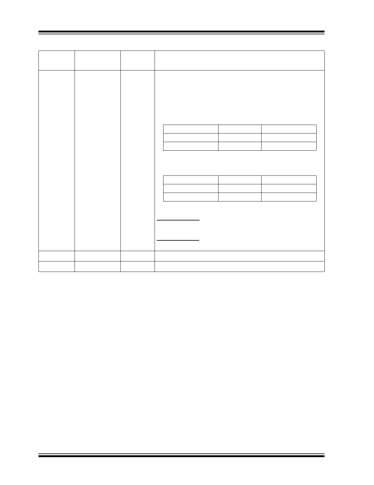
30
LED0 / NWAYEN
Ipu/O
LED Output: Programmable LED0 Output
Config ode: Latched as Auto-Negotiation Enable (register 0h, bit 12)
during power-up or reset. See
Strap-In option – KSZ8041NL
for
details.
The LED0 pin is programmable via register 1Eh bits [15:14] and is
defined as follows:
LED Mode = [00]
LED Mode = [01]
LED Mode = [10]
Reserved
LED Mode = [11]
Reserved
TABLE 2-1:
KSZ8041NL PIN DESCRIPTION (CONTINUED)
Pin Number
Symbol
Buffer Type
(
Note 2-1
)
Description
Link/Activity
Pin State
LED Definition
No Link
H
OFF
Link
L
ON
Activity
Toggle
Blinking
Link/Activity
Pin State
LED Definition
No Link
H
OFF
Link
L
ON
KSZ8041NL/RNL
DS00002245B-page 10
2017 Microchip Technology Inc.
Note 2-1
P = Power supply
Gnd = Ground
I = Input
O = Output
I/O = Bi-directional
Ipd = Input with internal pull-down (40K ±30%)
Ipu = Input with internal pull-up (40K ±30%)
Opu = Output with internal pull-up (40K ±30%)
Ipu/O = Input with internal pull-up (40K ±30%) during power-up/reset; output pin otherwise.
Ipd/O = Input with internal pull-down (40K ±30%) during power-up/reset; output pin otherwise.
Note 2-2
MII Rx mode: The RXD[3:0] bits are synchronous with RXCLK. When RXDV is asserted, RXD[3:0]
presents a valid data to the MAC through the MII. RXD[3:0] is invalid when RXDV is deasserted.
Note 2-3
RMII Rx mode: The RXD[1:0] bits are synchronous with REF_CLK. For each clock period in which
CRS_DV is asserted, two bits of recovered data are sent from the PHY.
Note 2-4
MII Tx mode: The TXD[3:0] bits are synchronous with TXCLK. When TXEN is asserted, TXD[3:0]
presents a valid data from the MAC through the MII. TXD[3..0] has no effect when TXEN is
deasserted.
Note 2-5
RMII Tx mode: The TXD[1:0] bits are synchronous with REF_CLK. For each clock period in which
TX_EN is asserted, two bits of data are received by the PHY from the MAC.
31
LED1 / SPEED
Ipu/O
LED Output: Programmable LED1 Output
Config mode: Latched as SPEED (register 0h, bit 13) during power-
up or reset. See
Strap-In option – KSZ8041NL
for details.
The LED1 pin is programmable via register 1Eh bits [15:14] and is
defined as follows:
LED Mode = [00]
LED Mode = [01]
LED Mode = [10]
Reserved
LED Mode = [11]
Reserved
32
RST#
I
Chip Reset (active low)
PADDLE
GND
Gnd
Ground
TABLE 2-1:
KSZ8041NL PIN DESCRIPTION (CONTINUED)
Pin Number
Symbol
Buffer Type
(
Note 2-1
)
Description
Speed
Pin State
LED Definition
10BT
H
OFF
100BT
L
ON
Activity
Pin State
LED Definition
No Activity
H
OFF
Activity
Toggle
Blinking