
2001 Microchip Technology Inc.
Preliminary
DS41116B-page 1
FEATURES
Security
• Two programmable 64-bit encryption keys
• 16/32-bit bi-directional challenge and response
using one of two keys
• Programmable 32-bit serial number
• Three IFF encryption algorithms
Operating
• Selectable baud rate
• Anti-collision of multiple transponders
• Intelligent damping for high Q LC-circuits
• Asynchronous transponder communication
Other
• 64-bit user EEPROM
Typical Applications
• Access control systems
• Automotive immobilizers
• Electronic door locks (Home/Office/Hotel)
• Burglar alarm systems
• Proximity access control
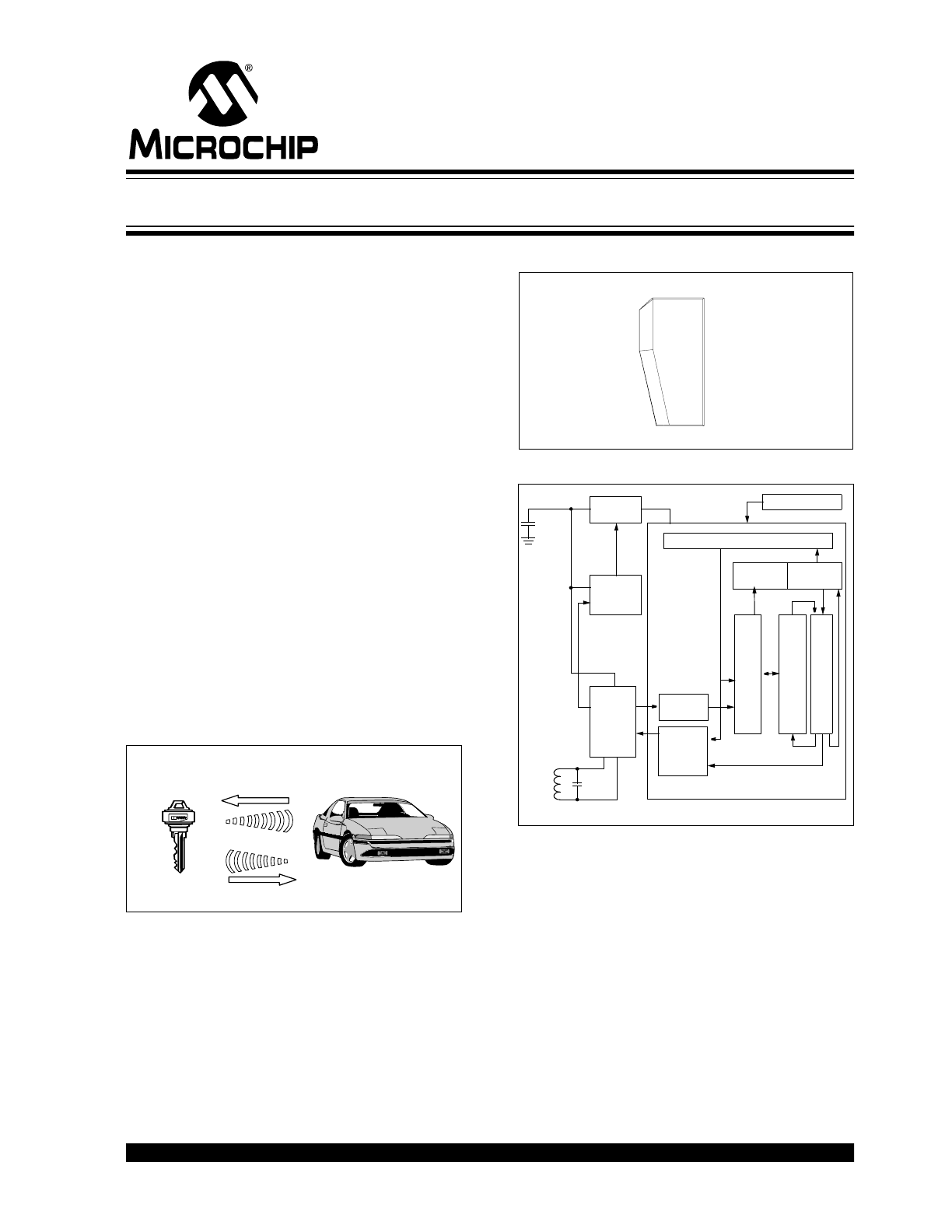
HCS410 IMMOBILIZER
TRANSPONDER
PACKAGE TYPES
BLOCK DIAGRAM
GENERAL DESCRIPTION
The HCS410/WM is a transponder device designed for
secure entry systems. The HCS410/WM utilizes bi-
directional challenge-and-response for logical and
physical access control.
The HCS410/WM integrates an LC-resonant circuit
with the HCS410 silicon into a leadless SOT-385 pack-
age.
Response
Crypto Read/Write
Transponder
Immobilizer
Base Station Unit
125KHz AM
Challenge
H
C
S
41
0/W
M
SOT385
Oscillator
Configuration Register
Power
Control
Wakeup
Logic
Address
Decoding EEPROM
PPM
Detector
PPM
Encoder
T
ranspond
er
Circ
u
itry
Cont
ro
l Logic
and Count
ers
Enc
rypt
ion
Logic
Regist
er
V
DD
125kHZ
C
RES
L
RES
C
POOL
*Secure Learn patent pending.
HCS410/WM
K
EE
L
OQ
®
Crypto Read/Write Transponder Module
K
EE
L
OQ
is a registered trademark of Microchip Technology, Inc.
Microchip’s Secure Data Products are covered by some or all of the following patents:
Code hopping encoder patents issued in Europe, U.S.A., and R.S.A. — U.S.A.: 5,517,187; Europe: 0459781; R.S.A.: ZA93/4726
Secure learning patents issued in the U.S.A. and R.S.A. — U.S.A.: 5,686,904; R.S.A.: 95/5429

HCS410/WM
DS41116B-page 2
Preliminary
2001 Microchip Technology Inc.
1.0
SYSTEM OVERVIEW
1.1
Key Terms
• Anticollision – Allows multiple transponders to be
in the magnetic field simultaneously and be veri-
fied individually.
• Encoder Key – A unique 64-bit key generated and
programmed into the encoder during the manu-
facturing process. The encoder keycontrols the
encryption algorithm and is stored in EEPROM on
the transponder device.
• IFF – Identify friend or foe is a means of validating
a token. A decoder sends a random challenge to
the token and checks that the response of the
token is a valid response.
• K
EE
L
OQ
Encryption Algorithm – The high security
level of the HCS410/WM is based on the patented
K
EE
L
OQ
technology. A block cipher encryption
algorithm based on a block length of 32 bits and a
key length of 64 bits is used. The algorithm
obscures the information in such a way that even
if the unencrypted/challenge information differs by
only one bit from the information in the previous
challenge, the next coded response will be totally
different. Statistically, if only one bit in the 32-bit
string of information changes, approximately
50 percent of the coded transmission will change.
• Learn – The HCS product family facilitates sev-
eral learning strategies to be implemented on the
decoder.
• Manufacturer’s Code – A 64-bit word, unique to
each manufacturer, used to produce a unique
encoder key in each transmitter (encoder).
• Transport Code – A 32-bit transport code needs to
be given before the HCS410/WM can be induc-
tively programmed. This prevents accidental
programming of the HCS410.
1.2
K
EE
L
OQ
IFF
The HCS410/WM is an IFF transponder for verification
of a token. In IFF mode the HCS410/WM is ideally
suited for authentication of a key before disarming a
vehicle immobilizer. Once the key has been inserted in
the car’s ignition the decoder would inductively poll the
key, validating it before disarming the immobilizer.
IFF validation of the token involves a random challenge
being sent by a decoder to a token. The token then
generates a response to the challenge and sends this
response to the decoder (Figure 1-1). The decoder cal-
culates an expected response using the same chal-
lenge. The expected response is compared to the
response received from the token. If the responses
match, the token is identified as a valid token and the
decoder can take appropriate action.
The HCS410/WM can do either 16 or 32-bit IFF. The
HCS410/WM has two encryption algorithms that can
be used to generate a response to a challenge. In addi-
tion there are up to two encoder keys that can be used
by the HCS410/WM. Typically each HCS410/WM will
be programmed with a unique encoder key(s).
In IFF mode, the HCS410/WM will wait for a command
from the base station and respond to the command.
The command can either request a read/write from
user EEPROM or an IFF challenge response. A given
16 or 32-bit challenge will produce a unique 16/32-bit
response, based on the IFF key and IFF algorithm
used.
FIGURE 1-1:
BASIC OPERATION OF AN IFF TOKEN
IFF Key
Serial Number
K
EE
L
OQ
IFF
Algorithm
Serial Number
EEPROM Array
Challenge Received from Decoder
Response
Read by Decoder
2001 Microchip Technology Inc.
Preliminary
DS41116B-page 3
HCS410/WM
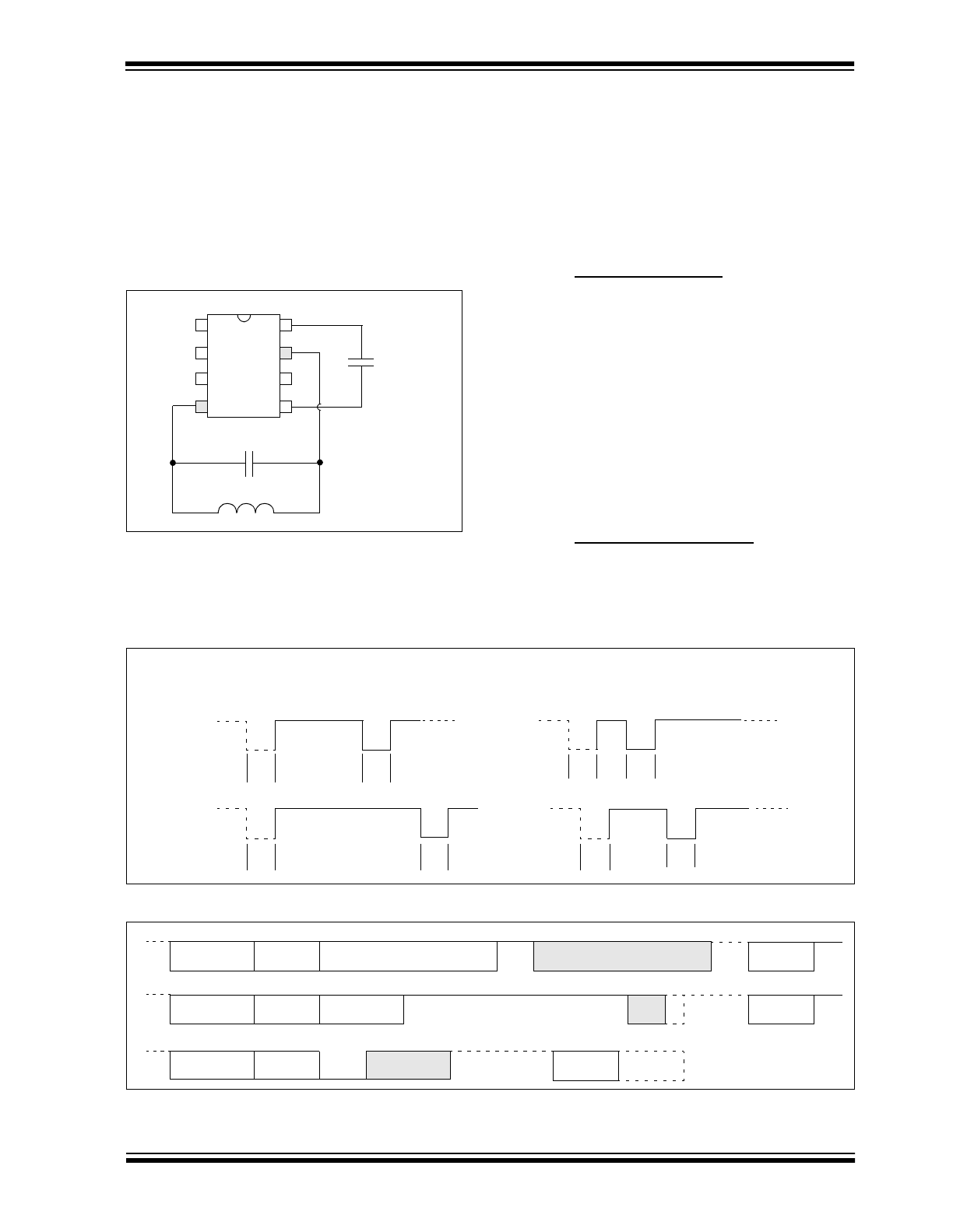
2.0
DEVICE DESCRIPTION
Figure 2-1 shows the internal components of the
HCS410/WM. The resonant LC circuit has 2 functions:
• Inductive antenna for communications between
the HCS410 and the base station
• Power source to charge the pool capacitor. The
pool capacitor functions as a battery when the
HCS410/WM is used.
FIGURE 2-1:
TRANSPONDER CIRCUIT
3.0
DEVICE OPERATION
The user can perform an IFF validation, write to the
user EEPROM and read from the user EEPROM. Each
operation consists of the decoder sending an opcode
and data while the HCS410/WM gives a response.
There are two IFF modes: IFF1 and IFF2. IFF1 allows
only one key IFF, while IFF2 allows two keys to be
used.
3.1
IFF Mode Activation
The HCS410/WM will enter IFF mode if the capacitor/
inductor resonant circuit generates a voltage large
enough so that the pool capacitor can power the
device. After the verified application of power and
elapse of the reset period, the device will start respond-
ing by pulsing the field with ACK pulses as shown in
Figure 3-3. This action will continue until the pulse train
is terminated by receiving a start signal of duration 2T
E
,
on the LC inputs before the next expected ACK pulse.
The device now enters the IFF mode and expects to
receive an ‘Opcode’ and a 0/16/32-bit Data-stream to
react on. The data rate (T
E
) is determined by the Tran-
sponder Baud Select (IFFB) configuration option.
3.2
IFF Decoder Commands
As shown in Figure 3-1, a logic 1 and 0 are differenti-
ated by the time between two rising edges. A long
pulse indicates a 1; a short pulse, a 0.
FIGURE 3-1:
MODULATION FOR IFF COMMUNICATION
FIGURE 3-2:
OVERVIEW OF IFF OPERATION
1
8
2
3
4
7
6
5
C
POOL
HCS4
1
0
C
RES
L
RES
0
1
3 T
E
T
E
5 T
E
0
1
T
E
T
E
2 T
E
T
E
Start or
previous
bit
T
E
PPM Decoder Commands
PPM Encoder Response
Activate
Opcode
32/16-bit Challenge
32/16-bit IFF Response
Opcode
Activate
Opcode
16-bit Data
OK
Opcode
Activate
Opcode
16-bit Data
IFF
WRITE
READ
Opcode
HCS410/WM
DS41116B-page 4
Preliminary
2001 Microchip Technology Inc.
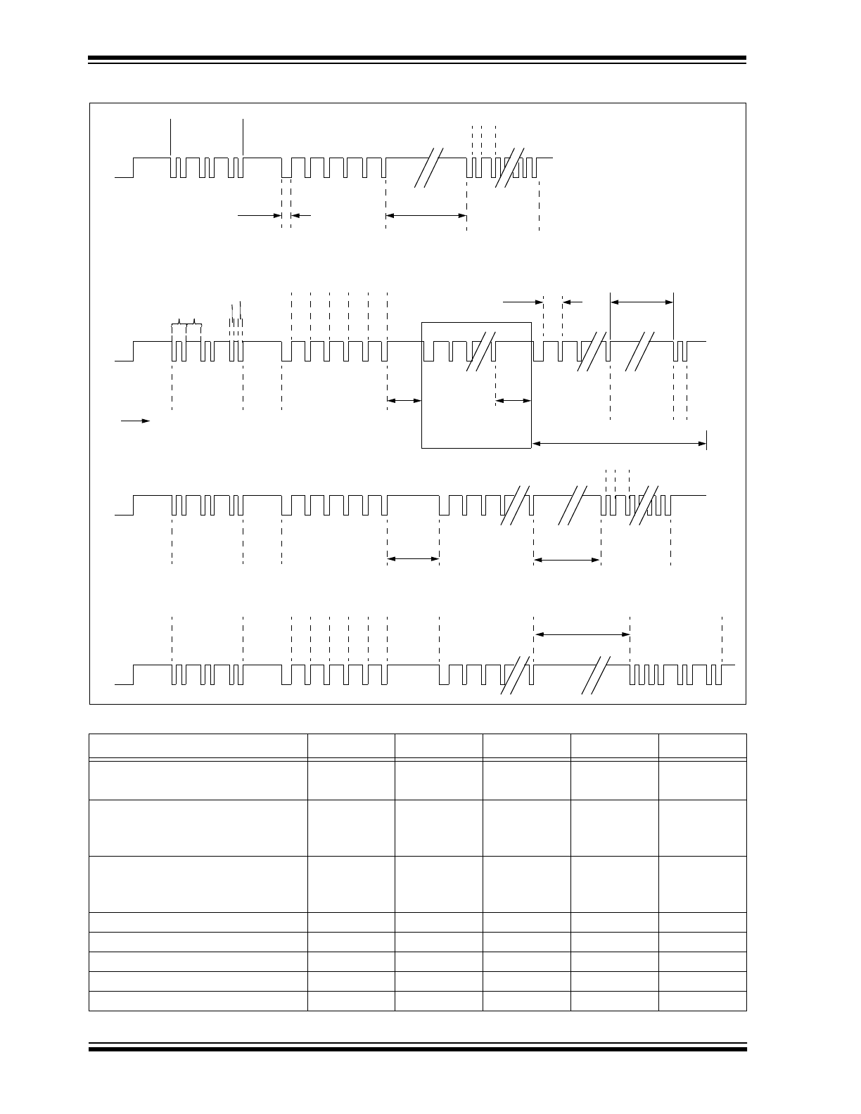
FIGURE 3-3:
DECODER IFF COMMANDS AND WAVEFORMS
ACK pulses
Opcode
Transport
Code
32 bits
ACK
Writing
bi
t0
bi
t1
bi
t2
bi
t3
bi
t4
T
BITC
T
E
Data
16 bits
T
OTD
T
TTD
T
WR
Only when writing Serial
Number, Config or IFF
programming
Serial number
1 to 32 bits
Encoder
Select
ACK
0
0
0
0
0
ACK pulses
Challenge
16/32 bits
Response
16/32 bits
ACK pulses
Opcode
T
OTD
Response
Start
T
RT
16 bits
0 1
ACK pulses
Read
Write/Program
Challenge
Encoder Select
2 T
E
Repeat 18 times for programming
3T
E
3T
E
T
E
T
WR
T
WR
Preamble
0 1
Preamble
TABLE 3-1:
IFF TIMING PARAMETERS
Parameter
Sym.
Min.
Typical
Max.
Units
Time Element
IFFB = 0
T
E
—
200
—
µ
s
PPM Command Bit Time
Data = 1
Data = 0
T
BITC
3.5
5.5
6
4
—
—
T
E
PPM Response Bit Time
Data = 1
Data = 0
T
BITR
—
—
3
2
—
—
T
E
PPM Command Minimum High Time
T
PMH
1.5
—
—
T
E
Response Time (Minimum for Read)
T
RT
6.5
—
—
ms
Opcode to Data Input Time
T
OTD
1.8
—
—
ms
Transport Code to Data Input Time
T
TTD
6.8
—
—
ms
IFF EEPROM Write Time (16 bits)
T
WR
—
16
30
ms

2001 Microchip Technology Inc.
Preliminary
DS41116B-page 5
HCS410/WM
3.3
HCS410/WM Responses
The responses from the HCS410/WM are in PPM for-
mat. See Figure 3-3 for additional information. Every
response from the HCS410 is preceded by a “2 bit pre-
amble” of 01
2
, and then 16/32 bits of data.
3.4
IFF Response
The 16/32-bit response to a 16/32-bit challenge, is
transmitted once, after which the device is ready to
accept another command. The same applies to the
result of a Read command. The opcode written to the
device specifies the challenge length and algorithm
used. The response always starts with a leading pre-
amble of 01
2
followed by the 16/32 bits of data.
3.5
IFF Write
The decoder can write to USER[0:3], SER[0:1], and the
configuration word in the EEPROM.
After the HCS410/WM has written the word into the
EEPROM, it will give two acknowledge pulses (T
E
wide
and T
E
apart) on the LC pins.
When writing to the serial number or configuration
word, the user must send the transport code before the
write will begin.
3.6
IFF Read
The decoder can read USER[0:3], SER[0:1], and the
configuration word in the EEPROM. After the data has
been read, the device is ready to receive a command
again.
Each read command is followed by a 16-bit data
response. The response always starts with a leading
preamble of 01
2
and then the 16-bits of data.
Note:
If the configuration word is written, the
device must be reset to allow the new con-
figuration settings to come into effect.
TABLE 3-1:
LIST OF IFF COMMANDS
Command
Description
Expected data In
Response
00000
Select HCS410/WM, used if Anti-
collision enabled
1 to 32 bits of the serial number
(SER)
Encoder select acknowledge if
SER match
00001
Read configuration word
None
16-bit configuration word
00010
Read low serial number
None
16 bits of serial number (SER0)
00011
Read high serial number
None
16 bits of serial number (SER1)
00100
Read user area 0
None
16 Bits of User EEPROM USR0
00101
Read user area 1
None
16 Bits of User EEPROM USR1
00110
Read user area 2
None
16 Bits of User EEPROM USR2
00111
Read user area 3
None
16 Bits of User EEPROM USR3
01000
Program HCS410 EEPROM
Transport code (32 bits); Com-
plete memory map: 18 x 16 bit
words (288 bits)
Write acknowledge pulse after
each 16-bit word, 288 bits trans-
mitted in 18 bursts of 16-bits
01001
Write configuration word
Transport code (32 bits); 16 Bit
configuration word
Write acknowledge pulse
01010
Write low serial number
Transport code (32 bits); Lower
16 bits of serial number (SER0)
Write acknowledge pulse
01011
Write high serial number
Transport code (32 bits); Higher
16 bits of serial number (SER1)
Write acknowledge pulse
01100
Write user area 0
16 Bits of User EEPROM USR0
Write acknowledge pulse
01101
Write user area 1
16 Bits of User EEPROM USR1
Write acknowledge pulse
01110
Write user area 2
16 Bits of User EEPROM USR2
Write acknowledge pulse
01111
Write user area 3
16 Bits of User EEPROM USR3
Write acknowledge pulse
1X000
IFF1 using key-1 and IFF
algorithm
32-Bit Challenge
32-Bit Response
1X001
IFF1 using key-1 and HOP
algorithm
32-Bit Challenge
32-Bit Response
1X100
IFF2 32-bit using key-2 and IFF
algorithm
32-Bit Challenge
32-Bit Response
1X101
IFF2 32-bit using key-2 and HOP
algorithm
32-Bit Challenge
32-Bit Response

HCS410/WM
DS41116B-page 6
Preliminary
2001 Microchip Technology Inc.
3.7
IFF Special Features
3.7.1
ANTI-COLLISION (ACOLI)
When the ACOLI bit is set in the configuration word,
anti-collision mode is entered. The HCS410/WM will
start sending ACK pulses when it enters a magnetic
field. The ACK pulses stop as soon as the HCS410/
WM detects a start bit from the decoder. A ‘select
encoder’ opcode (00000) is then sent out by the
decoder, followed by a 32-bit serial number. If the serial
number matches the HCS410/WM’s serial number, the
HCS410/WM will acknowledge with the acknowledge
sequence as shown in Figure 3-4. The HCS410/WM
can then be addressed as normal. If the serial number
does not match, the IFF encoder will stop transmitting
ACK pulses until it is either removed from the field or
the correct serial number is given.
FIGURE 3-4:
SERIAL NUMBER CORRECT
ACKNOWLEDGE SEQUENCE
3.7.2
INTELLIGENT DAMPING
If the IDAMP bit is set to 0, the HCS410/WM will clamp
the LC pins for 5 µs every 1/4 T
E
, whenever the
HCS410/WM is expecting data from the decoder. The
intelligent damping pulses start 64 T
E
after the
acknowledge pulses have been sent and continue for
64 T
E
. If the HSC410 detects data from the base station
while sending out damp pulses, the damp pulses will
continue to be sent. The damping will help the LC cir-
cuit resonance decay faster when the field is removed.
This can make high to low data field decay sharper.
LC0/1
T
E
T
E
3 T
E
3 T
E

2001 Microchip Technology Inc.
Preliminary
DS41116B-page 7
HCS410/WM
4.0
EEPROM ORGANIZATION AND
CONFIGURATION
The HCS410/WM has nonvolatile EEPROM memory
which is used to store user programmable options. This
information includes encoder keys, serial number, and
up to 64-bits of user information.
4.1
IFF Programming
Upon receiving a programming opcode and the trans-
port code, the EEPROM is erased. Thereafter, the first
16 bits of data can be written. After indicating that a
write command has been successfully completed the
device is ready to receive the next 16 bits. After a com-
plete memory map was received, it will be transmitted
in PPM format on the LC pins as 16-bit words.
After the EEPROM is erased, the configuration word is
reloaded. This results in oscillator tuning bits of 0000
being used during programming. When using IFF pro-
gramming, the user should read the configuration word
and store the oscillator bits in the memory map to be
programmed. A program command should be sent and
the next set of ACK pulses transmitted by the HCS410/
WM should be used to determine the T
E
. A second pro-
gram command can then be sent, and the device pro-
grammed using the T
E
just calibrated.
4.2
Encoder Key 1 and 2
In IFF operation, the HCS410/WM uses encoder key1
or key2 to generate the response to a challenge
received. The key or keys are created and pro-
grammed at the time of production using a key genera-
tion algorithm. Inputs to the key generation algorithm
are the serial number and a secret manufacturer’s
code. While a number of key generation algorithms are
supplied by Microchip, a user may elect to create their
own method of key generation. This may be done pro-
viding that the decoder is programmed with the same
means of creating the key for decryption purposes.
4.3
Transport Code
The least significant 32-bits of key2 are used as the
transport code. The transport code is used to write-pro-
tect the serial number, configuration word and prevent
accidental programming of the HCS410/WM.
4.4
Serial Number
There are 32 bits allocated for the serial number. The
serial number is meant to be unique for every transmit-
ter. The serial number can be programmed with a write
command.
4.5
User Data
The 64-bit user EEPROM can be reprogrammed and
read at any time using the IFF interface.
4.6
Configuration Data
The configuration data is used to select various
encoder options. Further explanations of each of the
bits are described in the following sections.
4.6.1
IDAMP: INTELLIGENT DAMPING
If IDAMP is set to ‘1’ intelligent damping is disabled.
4.6.2
IFF2: ENABLE IFF2 KEY
4.6.3
OSC: OSCILLATOR TUNING BITS
These bits allow the onboard oscillator to be tuned to
within 10% of the nominal oscillator speed over both
temperature and voltage.
4.6.4
IFFB: TRANSPONDER BAUD RATE
This selects the baud rate for IFF communications for
a T
E
of 200
µ
s.
4.6.5
ACOLI: ANTI-COLLISION
If ACOLI is set, the anti-collision operation during bidi-
rectional transponder mode (IFF) is enabled. This fea-
ture is useful in situations where multiple transponders
enter the magnetic field simultaneously.
TABLE 4-1:
CONFIGURATION OPTIONS
Symbol
Description
IDAMP
Intelligent Damping for High Q LC Tank.
IFF2
Enable IFF2 key
OSC0:3
Onboard Oscillator Tuning Bits
IFFB
Transponder Baud Rate
ACOLI
Anti Collision Communication Enable
TABLE 4-2:
OSCILLATOR TUNING
OSC
Description
1000
Fastest
1001
1010
•
•
•
1111
Faster
0000
Nominal
0001
0010
•
•
•
0110
Slower
0111
Slowest
HCS410/WM
DS41116B-page 8
Preliminary
2001 Microchip Technology Inc.
5.0
INTEGRATING THE
HCS410/WM INTO A SYSTEM
Use of the HCS410/WM in a system requires a compat-
ible decoder. This decoder is typically a microcontroller
with compatible firmware. Firmware routines that
accept transmissions from the HCS410/WM, decrypt
the code hopping portion of the data stream and per-
form IFF functions are available. These routines pro-
vide system designers the means to develop their own
decoding system.
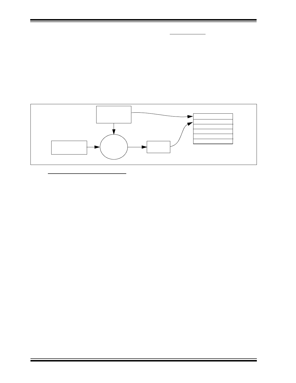
5.1
Key Generation
The serial number for each transmitter is programmed
by the manufacturer at the time of production. The
generation of the encoder key is done using a key gen-
eration algorithm (Figure 5-1). Typically, inputs to the
key generation algorithm are the serial number of the
transmitter or seed value, and a 64-bit manufacturer’s
code. The manufacturer’s code is chosen by the sys-
tem manufacturer and must be carefully controlled. The
manufacturer’s code is a pivotal part of the overall
system security.
FIGURE 5-1:
CREATION AND STORAGE OF ENCODER KEY DURING PRODUCTION
5.2
Receiver Learning an HCS410/WM
In order for a transmitter to be used with a decoder, the
transmitter must first be ‘learned’. Several learning
strategies can be followed in the decoder implementa-
tion. When a transmitter is learned by a decoder, it is
suggested that the decoder stores the serial number in
EEPROM. The decoder must keep track of these
values for every transmitter that is learned.
The maximum number of transmitters that can be
learned is a function of how much EEPROM memory
storage is available. The decoder must also store the
manufacturer’s code in order to learn an HCS410/WM,
since this value will not change in a typical system, it is
usually stored as part of the microcontroller ROM code.
Storing the manufacturer’s code as part of the ROM
code is also better for security reasons.
Transmitter
Manufacturer’s
Serial Number or
Code
Encoder
Key
Key
Generation
Algorithm
Serial Number
Encoder Key
Sync Counter
.
.
.
HCS410/WM EEPROM Array
Seed
2001 Microchip Technology Inc.
Preliminary
DS41116B-page 9
HCS410/WM
FIGURE 5-2:
TYPICAL IFF LEARN
SEQUENCE
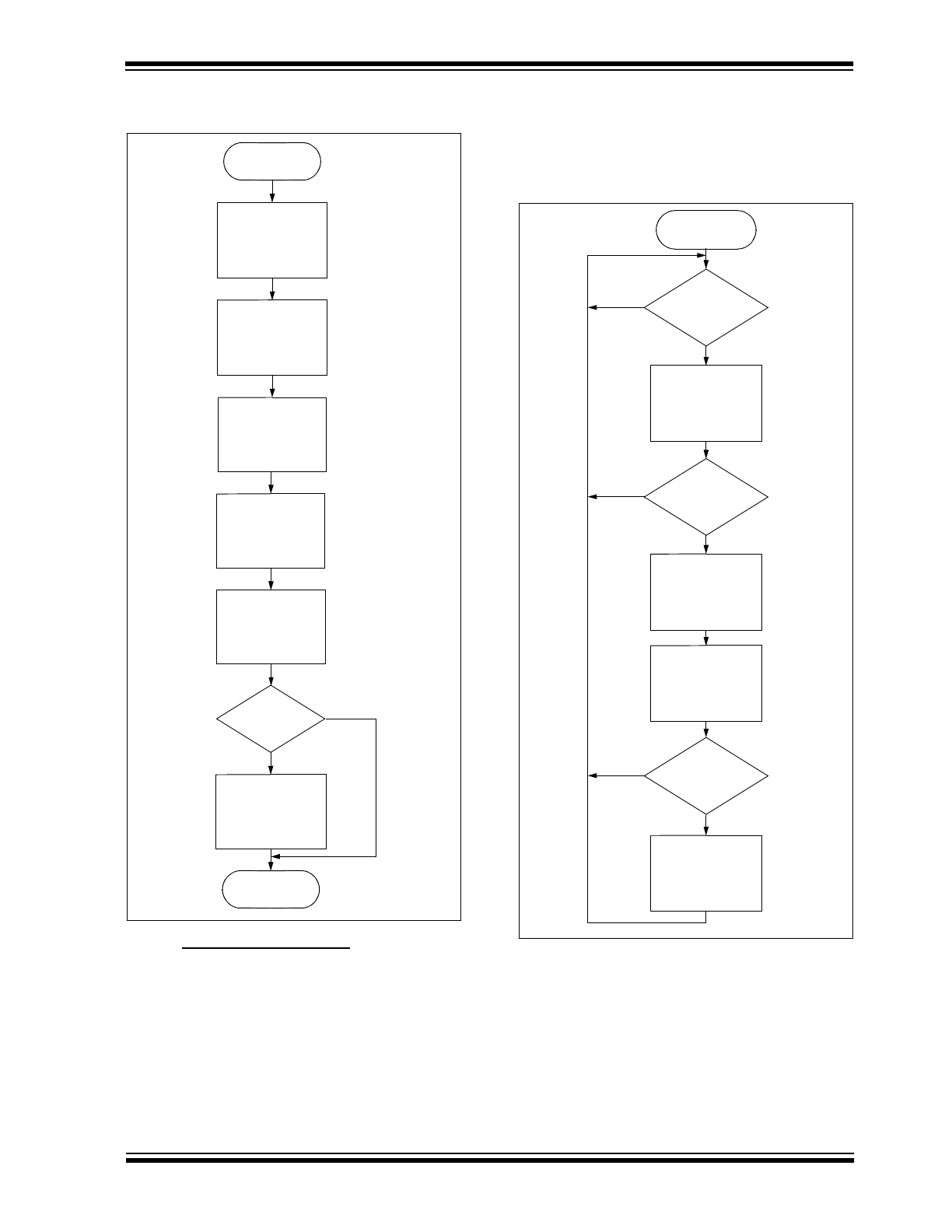
5.3
IFF Decoder Operation
In a typical IFF decoder, the key generation on the
decoder side is done by reading the serial number from
a token and combining that with the manufacturer’s
code to recreate the encoder key that is stored on the
token. The decoder polls for the presence of a token.
Once detected the decoder reads the serial number. If
the token has been learned, the decoder sends a chal-
lenge and reads the token’s response. The decoder
uses the encoder key stored in EEPROM to decrypt the
response. The decrypted response is compared to the
challenge. If they match, then identification was suc-
cessful and the appropriate response is generated.
FIGURE 5-3:
TYPICAL IFF DECODER
OPERATION
Enter Learn
Wait for token
to be detected
Read
Generate Key
From Serial
Perform IFF
with Token
Compare Token
and expected
response
Token and
Response
Equal?
Exit
Serial Number
No
Yes
Learn successful
Serial number
Encoder key
Number
Store:
Mode
Start
Token
Detected?
Read Serial
Does
Serial Number
Match?
Send Challenge
and Read
Decrypt the
Response
Does
Challenge &
Match?
Execute
No
No
No
Yes
Yes
Yes
Response
Number
Decrypt response
Command
HCS410/WM
DS41116B-page 10
Preliminary
2001 Microchip Technology Inc.
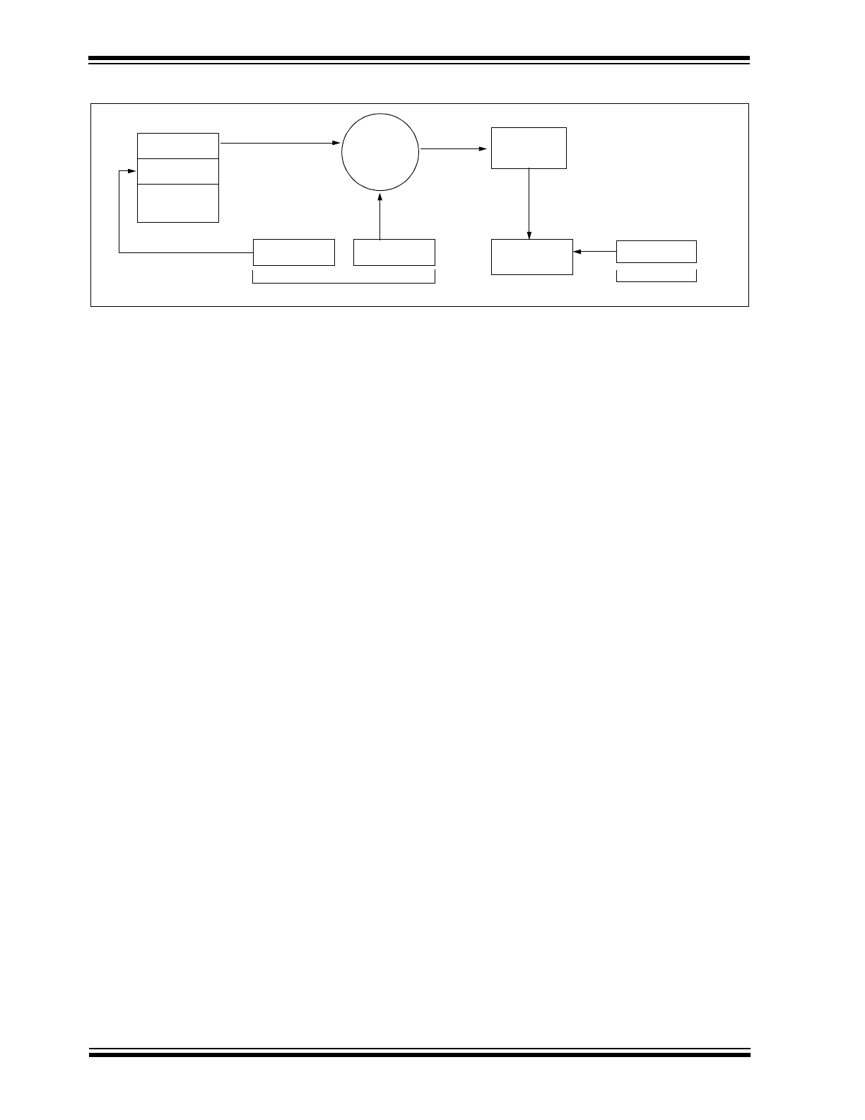
FIGURE 5-4:
BASIC OPERATION OF AN IFF RECEIVER (DECODER)
IFF Key
Serial Number
K
EE
L
OQ
IFF
Algorithm
Decrypted
EEPROM Array
Manufacturer
Code
Serial Number
Response
Check for
Match
Response
Challenge
Information read from HCS410/WM
Written to HCS410/WM