

2017 Microchip Technology Inc.
DS20005730A-page 1
MIC1555/57
Features
• +2.7V to +18V Operation
• Low Current
- <1 μA Typical Shutdown Mode (MIC1557)
- 200 μA Typical (TRG and THR Low) at 3V
Supply
• Timing from Microseconds to Hours
• “Zero” Leakage Trigger and Threshold Inputs
• 50% Square Wave with One Resistor, One
Capacitor
• Threshold Input Precedence Over Trigger Input
• <15Ω Output On-Resistance
• No Output Cross-Conduction Current Spikes
• <0.005%/°C Temperature Stability
• <0.055%/V Supply Stability
• 10-pin Ultra-Thin DFN Package (2 mm × 2 mm ×
0.4 mm)
• Small SOT-23-5 Surface Mount Package
Applications
• Precision Timer
• Pulse Generation
• Sequential Timing
• Time-Delay Generation
• Missing Pulse Detector
• Micropower Oscillator to 5 MHz
• Charge-Pump Driver
• LED Blinker
• Voltage Converter
• Linear Sweep Generator
• Variable Frequency and Duty Cycle Oscillator
General Description
The MIC1555 IttyBitty CMOS RC timer/oscillator and
MIC1557 IttyBitty CMOS RC oscillator are designed to
provide rail-to-rail pulses for precise time delay or
frequency generation.
These devices are similar in function to the industry
standard “555”, without a frequency control (FC) pin or
an open-collector discharge (D) pin. The threshold pin
(THR) has precedence over the trigger (TRG) input,
ensuring that the BiCMOS output is off when TRG is
high.
The MIC1555 can be used as an astable (oscillator) or
monostable (one-shot) with separate threshold and
trigger inputs. In the one-shot mode, the output pulse
width is precisely controlled by an external resistor and
a capacitor. Time delays may be accurately controlled
from microseconds to hours. In the oscillator mode, the
output is used to provide precise feedback, with a
minimum of one resistor and one capacitor producing a
50% duty cycle square wave.
The MIC1557 is designed for astable (oscillator)
operation only, with a chip select/reset (CS) input for
low power shut-down. One resistor and one capacitor
provide a 50% duty cycle square wave. Other duty
cycle ratios may be produced using two diodes and two
resistors.
The MIC1555/7 are powered from a +2.7V to +18V
supply voltage and are rated for –40°C to +85°C
ambient temperature range. The MIC1555/7 are
available in SOT-23-5, and thin SOT23-5 5-pin
packages. A low profile, ultra-thin UTDFN version of
the MIC1555 (with chip select) is also available.
IttyBitty RC Timer/Oscillator
MIC1555/57
DS20005730A-page 2
2017 Microchip Technology Inc.
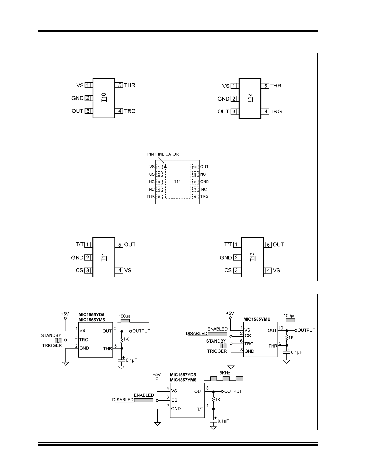
Package Types
Typical Application Circuits
MIC1555
5-P
IN
SOT-23 (M5)
(T
OP
V
IEW
)
MIC1555
5-P
IN
TSOT-23
(T
OP
V
IEW
)
MIC1555
10-P
IN
UTDFN (MU)
(T
OP
V
IEW
)
MIC1555
5-P
IN
SOT-23 (M5)
(T
OP
V
IEW
)
MIC1555
5-P
IN
SOT-23 (M5)
(T
OP
V
IEW
)
MIC1555
M
ONOSTABLE
(O
NE
-S
HOT
)
MIC1555
M
ONOSTABLE
W
ITH
E
NABLE
MIC1557
A
STABLE
(O
SCILLATOR
)
2017 Microchip Technology Inc.
DS20005730A-page 3
MIC1555/57
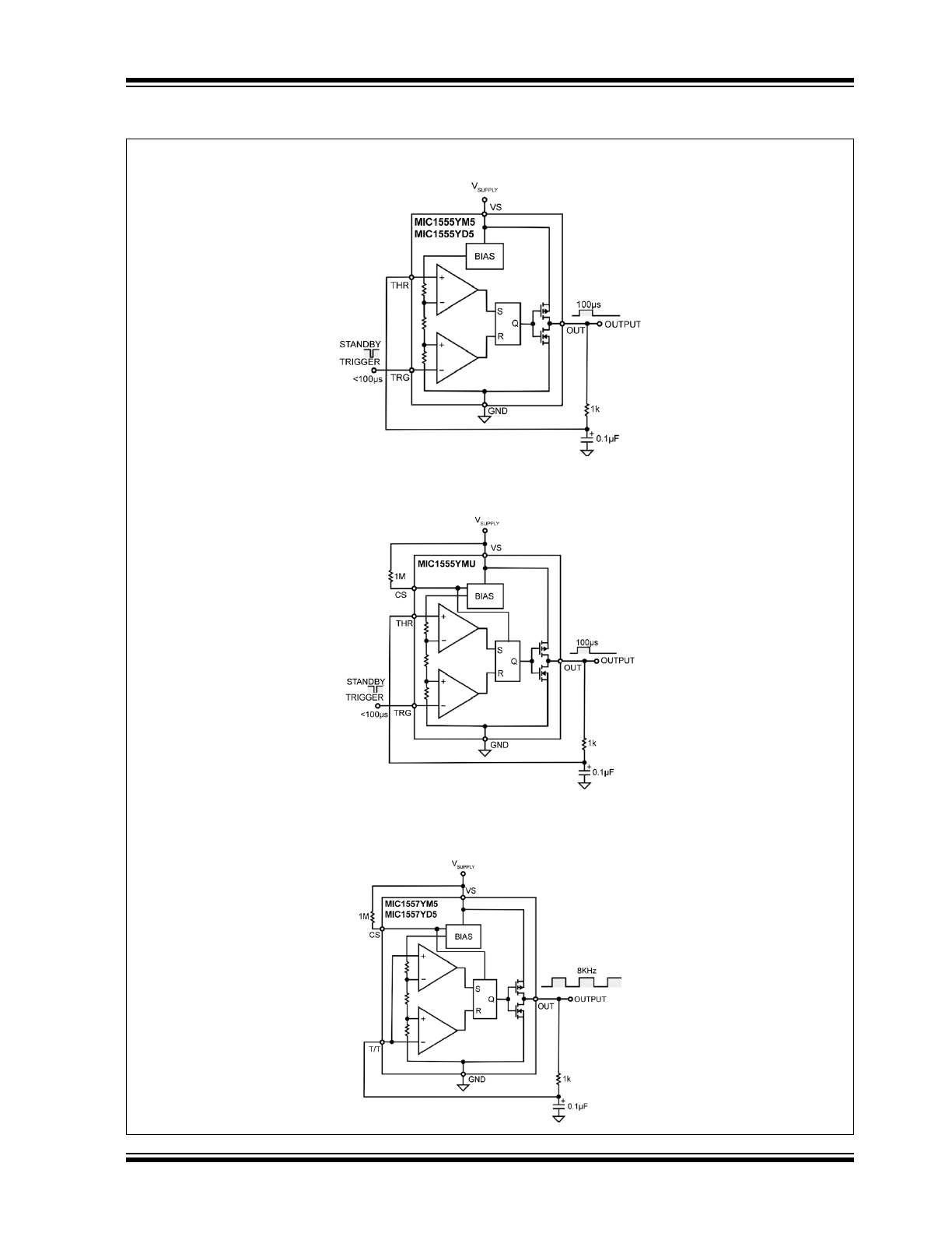
Functional Diagrams
MIC155YM5/MIC155YD5 B
LOCK
D
IAGRAM
WITH
E
XTERNAL
C
OMPONENTS
(M
ONOSTABLE
C
ONFIGURATION
)
MIC1555YMU B
LOCK
D
IAGRAM
WITH
E
XTERNAL
C
OMPONENTS
(M
ONOSTABLE
C
ONFIGURATION
)
MIC1557YM5/MIC1557YD5 B
LOCK
D
IAGRAM
WITH
E
XTERNAL
C
OMPONENTS
(A
STABLE
C
ONFIGURATION
)

MIC1555/57
DS20005730A-page 4
2017 Microchip Technology Inc.
1.0
ELECTRICAL CHARACTERISTICS
Absolute Maximum Ratings †
Supply Voltage (V
S
)...................................................................................................................................................+22V
Threshold Voltage (V
THR
, V
T/T
) .................................................................................................................................+22V
Trigger Voltage (V
TGR
, V
T/T
) .....................................................................................................................................+22V
ESD HBM Rating (
Note 1
)..........................................................................................................................................2 kV
ESD MM Rating (
Note 1
)...........................................................................................................................................200V
Operating Ratings ‡
Supply Voltage (V
S
).................................................................................................................................... +2.7V to +18V
†
Notice: Stresses above those listed under “Absolute Maximum Ratings” may cause permanent damage to the device.
This is a stress rating only and functional operation of the device at those or any other conditions above those indicated
in the operational sections of this specification is not intended. Exposure to maximum rating conditions for extended
periods may affect device reliability.
‡ Notice:
The device is not guaranteed to function outside its operating ratings.
Note 1:
Devices are ESD protected, however handling precautions recommended.
2017 Microchip Technology Inc.
DS20005730A-page 5
MIC1555/57
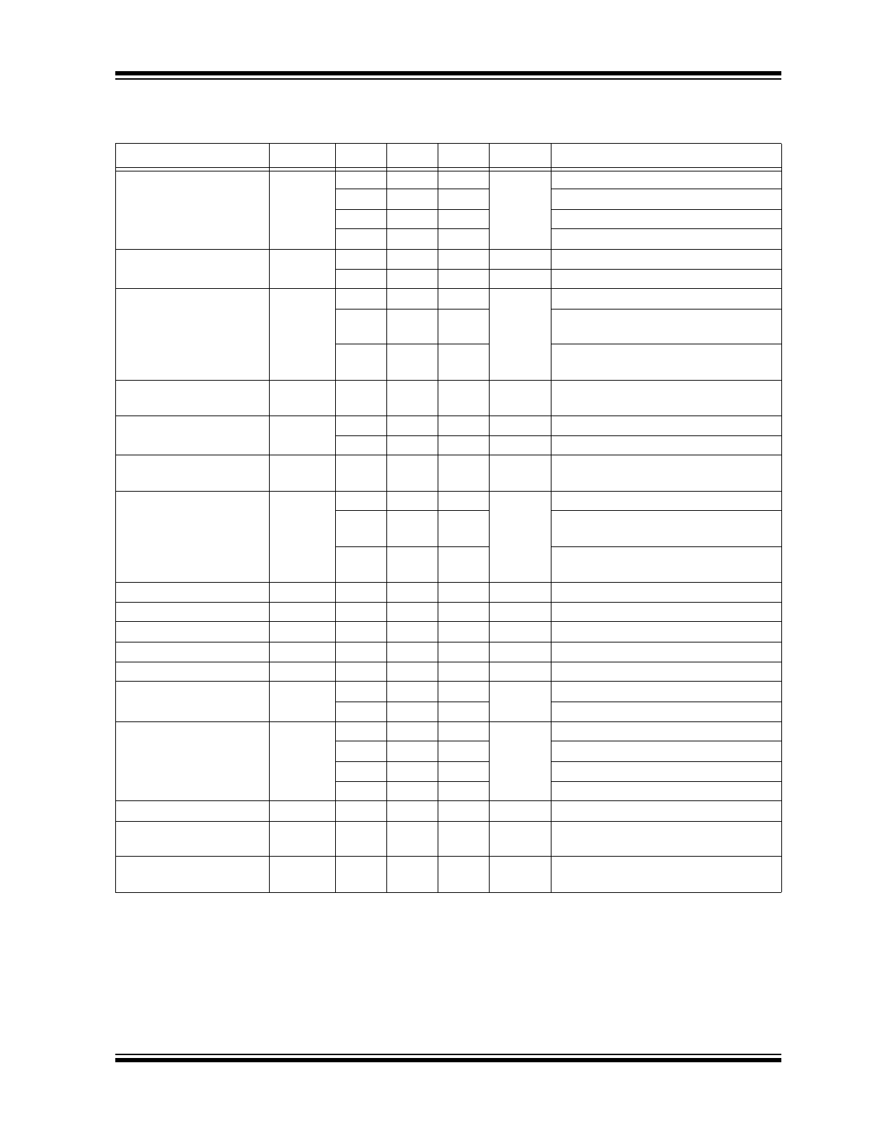
TABLE 1-1:
ELECTRICAL CHARACTERISTICS (
Note 1
)
Electrical Characteristics:
T
A
= +25°C, bold values indicate –40°C ≤ T
A
≤ +85°C, unless noted.
Parameter
Symbol
Min.
Typ.
Max.
Units
Conditions
Supply Current
I
S
—
240
300
µA
MIC1555, V
S
= 5V
—
255
315
MIC1557, V
S
= 5V
—
350
400
MIC1555, V
S
= 15V
—
370
420
MIC1557, VS = 15V
Monostable Timing
Accuracy
—
—
2
—
%
R
A
= 10 kΩ, C =0.1 μF, V
S
= 5V
858
—
1161
µs
R
A
= 10 kΩ, C =0.1 μF, V
S
= 5V
Monostable Drift Over
Temperature
—
—
100
—
ppm/°C
V
S
= 5V, –55°C ≤ T
A
≤ +125°C (
Note 2
)
—
150
—
V
S
= 10V, –55°C ≤ T
A
≤ +125°C
(
Note 2
)
—
200
—
V
S
= 15V, –55°C ≤ T
A
≤ +125°C
(
Note 2
)
Monostable Drift Over
Supply
—
—
0.5
—
%/V
V
S
= 5V to 15V (
Note 2
)
Astable Timing Accuracy
—
—
2
—
%
R
A
= R
B
= 10 kΩ, C = 0.1 μF, V
S
= 5V
1717
—
2323
µs
R
A
= R
B
= 10 kΩ, C = 0.1 μF, V
S
= 5V
Maximum Astable
Frequency
—
—
—
5
MHz
R
T
= 1 kΩ, C
T
= 47 pF, V
S
= 8V
Astable Drift Over
Temperature
—
—
100
—
ppm/°C
V
S
= 5V, –55°C ≤ T
A
≤ +125°C (
Note 2
)
—
150
—
V
S
= 10V, –55°C ≤ T
A
≤ +125°C
(
Note 2
)
—
200
—
V
S
= 15V, –55°C ≤ T
A
≤ +125°C
(
Note 2
)
Astable Drift Over Supply
—
—
0.5
—
%/V
V
S
= 5V to 15V (
Note 2
)
Threshold Voltage
—
61
67
72
%/V
S
V
S
= 15V
Trigger Voltage
—
27
32
37
%/V
S
V
S
= 15V
Trigger Current
—
—
—
50
nA
V
S
= 15V
Threshold Current
—
—
—
50
nA
V
S
= 15V
Chip Select
—
50
67
72
%/V
S
On > two-thirds of V
S
28
33
50
Off < one-third of V
S
Output Voltage Drop
—
—
0.3
1.25
V
V
S
= 15V, I
SINK
= 20 mA
—
0.08
0.5
V
S
= 5V, I
SINK
= 20 mA
14.1
14.7
—
V
S
= 15V, I
SOURCE
= 20 mA
3.8
4.7
—
V
S
= 5V, I
SOURCE
= 20 mA
Supply Voltage
—
2.7
—
18
V
Functional Operation (
Note 2
)
Output Rise Time
—
—
15
—
ns
R
L
= 10 MΩ, C
L
= 10 pF, V
S
= 5V
(
Note 2
)
Output Fall Time
—
—
15
—
ns
R
L
= 10 MΩ, C
L
= 10 pF, V
S
= 5V
(
Note 2
)
Note 1:
Specification for packaged product only.
2:
Not tested.
MIC1555/57
DS20005730A-page 6
2017 Microchip Technology Inc.
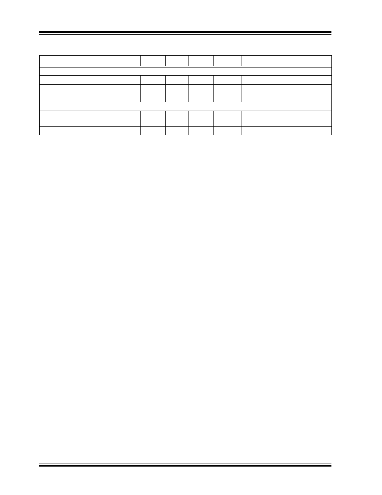
TEMPERATURE SPECIFICATIONS (
Note 1
)
Parameters
Sym.
Min.
Typ.
Max.
Units
Conditions
Temperature Ranges
Ambient Storage Temperature
T
S
–65
—
+150
°C
—
Lead Temperature
—
—
—
+300
°C
Soldering, 10 sec.
Ambient Temperature
T
A
–40
—
+85
°C
—
Package Thermal Resistance
Thermal Resistance SOT-23-5 and
TSOT-23-5
θ
JA
—
250
—
°C/W
—
Thermal Resistance 10-Ld UTDFN
θ
JA
—
90
—
°C/W
—
Note 1:
The maximum allowable power dissipation is a function of ambient temperature, the maximum allowable
junction temperature and the thermal resistance from junction to air (i.e., T
A
, T
J
,
JA
). Exceeding the
maximum allowable power dissipation will cause the device operating junction temperature to exceed the
maximum +125°C rating. Sustained junction temperatures above +125°C can impact the device reliability.
2017 Microchip Technology Inc.
DS20005730A-page 7
MIC1555/57
2.0
TYPICAL PERFORMANCE CURVES
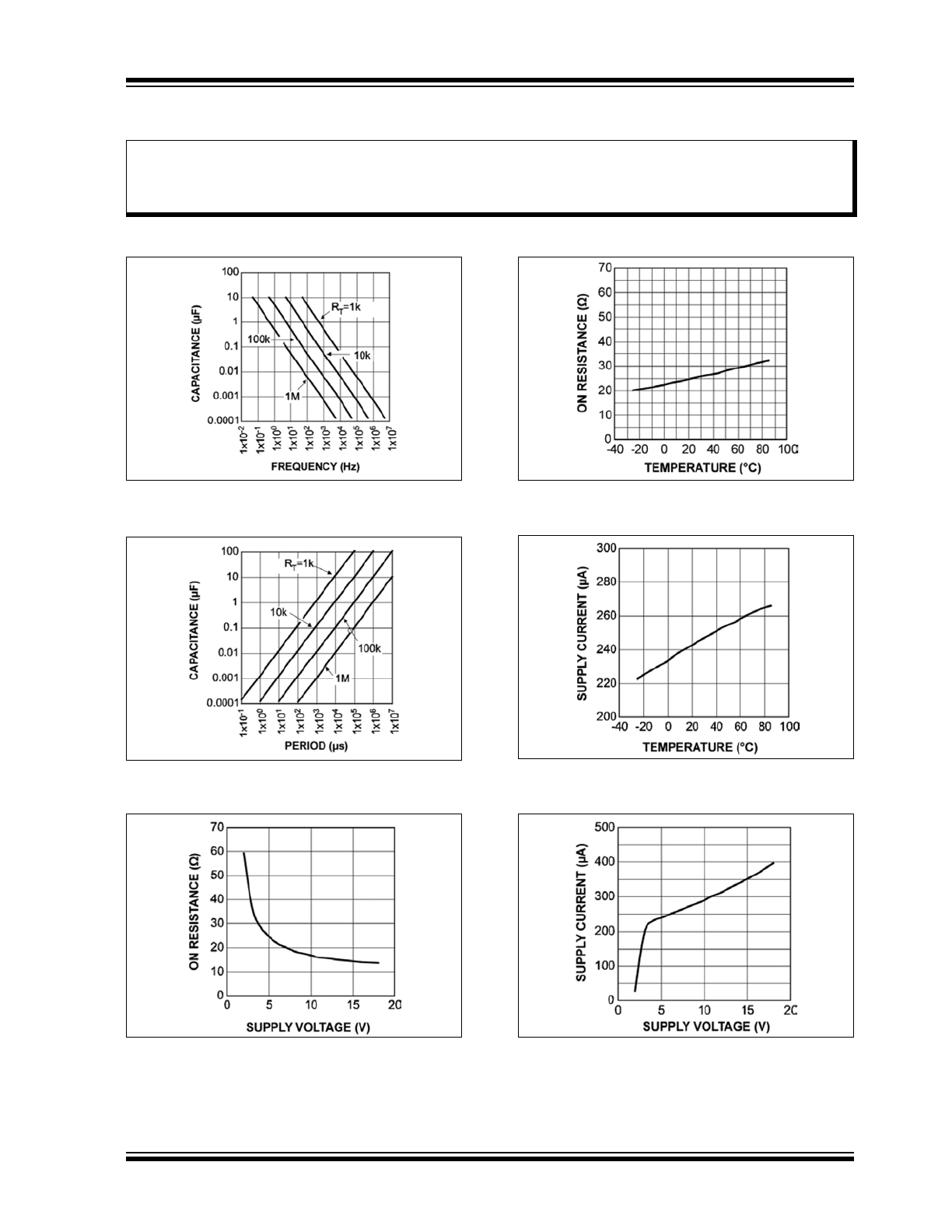
FIGURE 2-1:
Astable Frequency.
FIGURE 2-2:
Pulse Width.
FIGURE 2-3:
On Resistance vs. Supply
Voltage.
FIGURE 2-4:
On Resistance vs.
Temperature.
FIGURE 2-5:
Supply Current vs.
Temperature.
FIGURE 2-6:
Supply Current vs. Supply
Voltage.
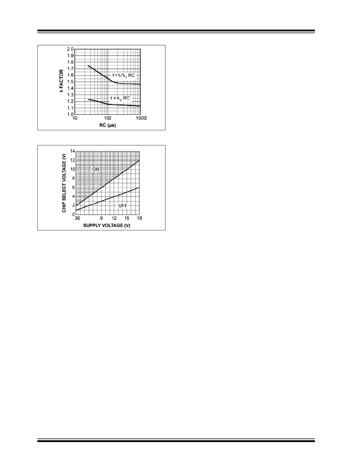
Note:
The graphs and tables provided following this note are a statistical summary based on a limited number of
samples and are provided for informational purposes only. The performance characteristics listed herein
are not tested or guaranteed. In some graphs or tables, the data presented may be outside the specified
operating range (e.g., outside specified power supply range) and therefore outside the warranted range.
MIC1555/57
DS20005730A-page 8
2017 Microchip Technology Inc.
FIGURE 2-7:
k Factors Times RC.
FIGURE 2-8:
MIC1555YMU and MIC1557
Chip Select vs. Supply Voltage.
2017 Microchip Technology Inc.
DS20005730A-page 9
MIC1555/57
3.0
PIN DESCRIPTIONS
The descriptions of the pins are listed in
Table 3-1
,
Table 3-2
, and .
TABLE 3-1:
PIN FUNCTION TABLE, MIC1555 SOT-23 AND TSOT-23
Pin Number
Pin Name
Description
1
VS
Supply (Input): +2.7V to +18V supply.
2
GND
Ground: Supply return.
3
OUT
Output: CMOS totem-pole output.
4
TRG
Trigger (Input): Sets output high. Active-low (at ≤2/3V
S
nominal).
5
THG
Threshold (Dominant Input): Sets output low. Active-high (at ≥2/3V
S
nominal).
TABLE 3-2:
PIN FUNCTION TABLE, MIC1555 UTDFN
Pin Number
Pin Name
Description
1
VS
Supply (Input): +2.7 to +18V supply.
2
CS
Chip Select/Reset (Input): Active-high at >2/3V
S
. Output off when low at <1/3V
S
. If chip
select functionality is not desired, CS may be connected directly to VS.
3, 4, 7, 9
NC
No Connect. This pin is not internally connected.
5
THR
Threshold (Dominant Input): Sets output low. Active-high (at ≥ 2/3V
S
nominal).
6
TRG
Trigger (Input): Sets output high. Active-low (at ≤2/3V
S
nominal).
8
GND
Ground. Supply return.
10
OUT
Output: CMOS totem-pole output
TABLE 3-3:
PIN FUNCTION TABLE, MIC1557 SOT-23 AND TSOT-23
Pin Number
Pin Name
Description
1
T/T
Trigger/Threshold (Input): Internally connected to both threshold and trigger functions.
When the voltage at this pin is ≤2/3V
S
, it will set the output high. When the voltage at
this pin is ≥2/3V
S
, it will set the output low.
2
GND
Ground: Supply return.
3
CS
Chip Select/Reset (Input): Active-high at >2/3V
S
. Output off when low at <1/3V
S
. If chip
select functionality is not desired, CS may be connected directly to VS.
4
VS
Supply (Input): +2.7 to +18V supply.
5
OUT
Output: CMOS totem-pole output.

MIC1555/57
DS20005730A-page 10
2017 Microchip Technology Inc.
4.0
FUNCTIONAL DESCRIPTION
The MIC1555/7 provides the logic for creating simple
RC timer or oscillator circuits.
The MIC1555 has separate THR (threshold) and TRG
(trigger) connections for monostable (one-shot) or
astable (oscillator) operation.
The MIC1557 has a single T/T (threshold and trigger)
connection for astable (oscillator) operation only. The
MIC1557 includes a CS (chip select/reset) control.
For more information, refer to the
Functional Diagrams
for MIC1555 and MIC1557.
4.1
Supply
Voltage supply (V
S
) is rated for +2.7V to +18V. An
external capacitor is recommended to decouple noise.
4.2
Resistive Divider
The resistive voltage divider is constructed of three
equal value resistors to produce 1/3V
S
and 2/3V
S
voltage for trigger and threshold reference voltages.
4.3
Chip Select/Reset (MIC1555YMU
and MIC1557 only)
Chip select/reset (CS) controls the bias supply to the
oscillator’s internal circuitry. CS must be connected to
CMOS logic-high or logic-low levels. Floating CS will
result in unpredictable operation. When the chip is
deselected, the supply current is less than 1 μA.
Forcing CS low resets the device by setting the flip flop,
forcing the output low. If Chip Select functionality is not
desired, CS may be connected directly to V
S
.
4.4
Threshold Comparator
The threshold comparator is connected to S (set) on
the RS flip-flop. When the threshold voltage (2/3V
S
) is
reached, the flip-flop is set, making the output low. THR
is dominant over TRG.
4.5
Trigger Comparator
The trigger comparator is connected to R (reset) on the
RS flip-flop. When TRG (trigger) goes below the trigger
voltage (1/3V
S
), the flip-flop resets, making the output
high.
4.6
Flip-Flop and Output
A reset signal causes Q to go low, turning on the
P-channel MOSFET and turning off the N-channel
MOSFET. This makes the output rise to nearly V
S
.
A set signal causes Q to go high, turning off the
P-channel MOSFET, and turning on the N-channel
MOSFET, grounding OUT.
4.7
Basic Monostable Operation
A momentary low signal applied to TRG causes the
output to go high. The external capacitor charges
slowly through the external resistor. When threshold
voltage (V
THR
) reaches 2/3V
S
, the output is switched
off, discharging the capacitor. During power-on, a
single pulse may be generated.
For more information, refer to the
Functional Diagrams
for MIC1555.
4.8
Basic Astable Operation
The MIC1557 starts with T/T low, causing the output to
go high. The external capacitor charges slowly through
the external resistor. When V
T/T
reaches 2/3V
S
(threshold voltage), the output is switched off, slowly
discharging the capacitor. When V
T/T
decreases to
1/3V
S
(trigger voltage), the output is switched on,
causing V
T/T
to rise again, repeating the cycle.
For more information, refer to the
Functional Diagrams
for MIC1557.