
© 2007 Microchip Technology Inc.
DS21618B-page 1
MCP2120
Features
• Supports with IrDA
®
Physical Layer Specification
(version 1.3)
• UART to IR Encoder/Decoder
- Interfaces with IrDA Compliant Transceivers
- Used with any UART, including standard
16550 UART and microcontroller UART
• Transmit/Receive formats supported:
- 1.63 µs
• Hardware or Software Baud rate selection
- Up to IrDA standard 115.2 kbaud operation
- Up to 312.5 kbaud operation (at 20 MHz)
- Low power mode
• Pb-free packaging
CMOS Technology
• Low-power, high-speed CMOS technology
• Fully static design
• Low voltage operation
• Commercial and Industrial temperature ranges
• Low power consumption
- < 1 mA @ 3.3V, 8 MHz (typical)
- 3 mA typical @ 5.0V when disabled
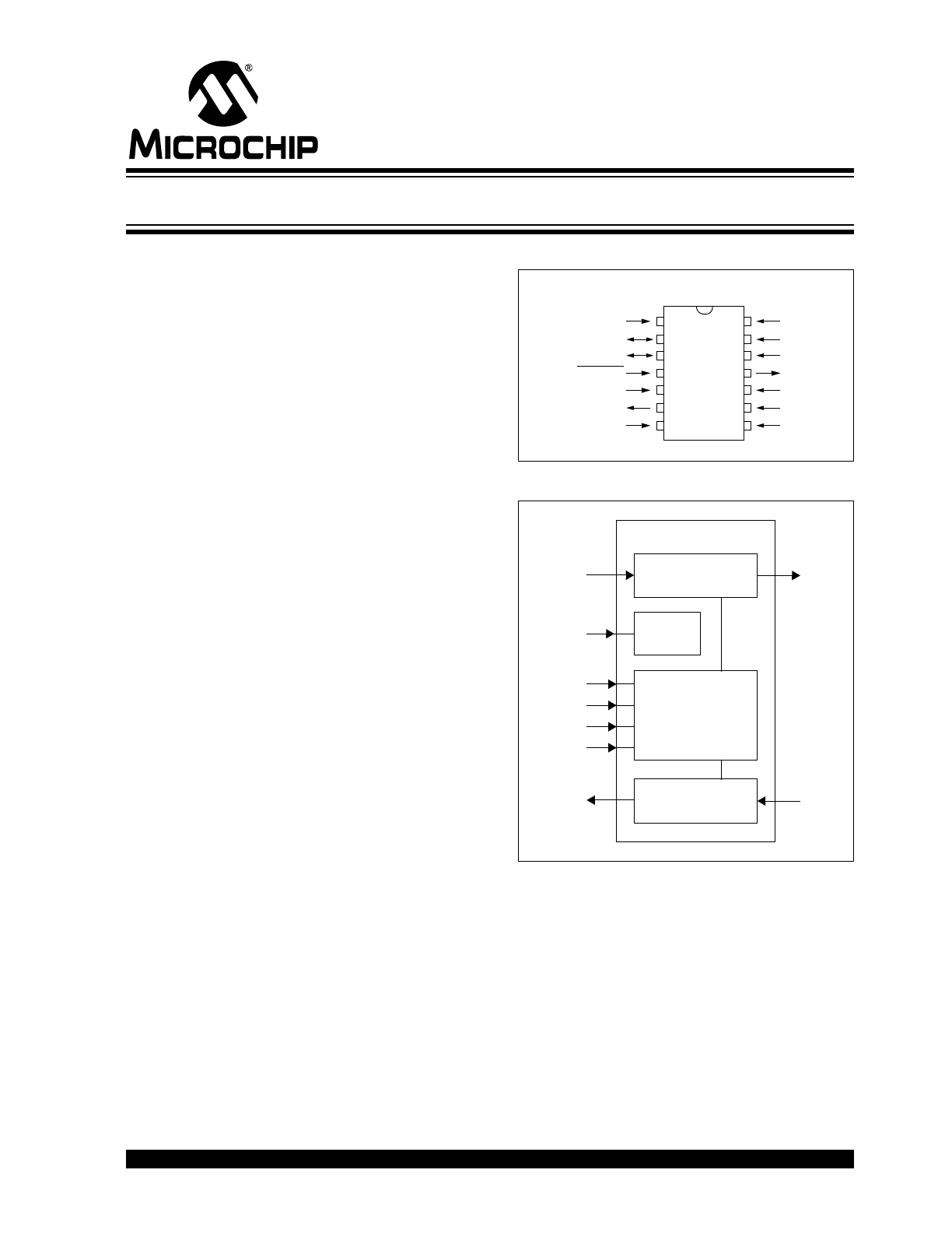
Pin Diagrams
Block Diagram
PDIP, SOIC
MC
P2120
V
DD
OSC1/CLKIN
OSC2
RESET
RXIR
TXIR
MODE
V
SS
EN
TX
RX
BAUD0
BAUD1
BAUD2
1
2
3
4
5
6
7
14
13
12
11
10
9
8
Decode
TX
TXIR
RX
RXIR
EN
MCP2120
Logic
Baud Rate
BAUD2
Generator
BAUD1
BAUD0
MODE
Encode
Infrared Encoder/Decoder

MCP2120
DS21618B-page 2
© 2007 Microchip Technology Inc.
NOTES:
© 2007 Microchip Technology Inc.
DS21618B-page 3
MCP2120
1.0
DEVICE OVERVIEW
This document contains device specific information for
the following device:
• MCP2120
This device is a low-cost, high-performance, fully-static
infrared encoder/decoder. This device sits between a
UART and an infrared (IR) optical transceiver.
The data received from a standard UART is encoded
(modulated), and output as electrical pulses to the IR
Transceiver. The IR Transceiver also receives data
which it outputs as electrical pulses. The MCP2120
decodes (demodulates) these electrical pulses and
then the data is transmitted by the MCP2120 UART.
This modulation and demodulation method is
performed in accordance with the IrDA standard.
Typically a microcontroller interfaces to the IR encoder/
decoder.
Infrared communication is a wireless two-way data
connection using infrared light generated by low-cost
transceiver signaling technology. This provides reliable
communication between two devices.
Infrared technology offers:
• Universal standard for connecting portable
computing devices
• Easy, effortless implementation
• Economical alternative to other connectivity
solutions
• Reliable, high speed connection
• Safe to use in any environment; can even be used
during air travel
• Eliminates the hassle of cables
• Allows PC’s and non-PC’s to communicate to
each other
• Enhances mobility by allowing users to easily
connect
1.1
Applications
The MCP2120 is a stand–alone IrDA Encoder/Decoder
product.
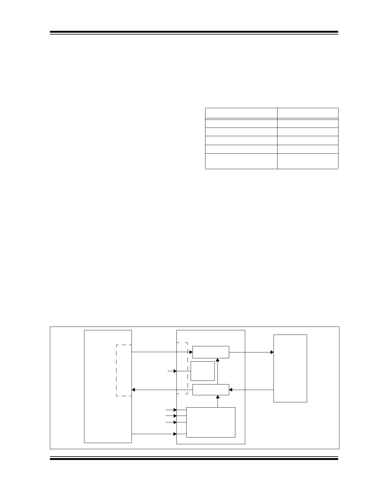
Figure 1-1
shows a typical application block
diagram.
Table 1-2
shows the pin definitions in the user
(normal) mode of operation.
TABLE 1-1:
MCP2120 FEATURES
OVERVIEW
FIGURE 1-1:
System Block Diagram
Features
MCP2120
Serial Communications:
UART, IR
Baud Rate Selection:
Hardware/Software
Low Power Mode:
Yes
Resets: (and Delays)
Wake-up (DRT)
Packages:
14-pin DIP
14-pin SOIC
Encode
Decode
TX
TXIR
RX
RXIR
EN
MCP2120
Micro–
TX
RX
Optical
UAR
T
TXD
RXD
Power
Down
Baud Rate
BAUD2
Generator
BAUD1
BAUD0
MODE
I/O
Controller
Logic
(S/W Mode)
Transceiver
MCP2120
DS21618B-page 4
© 2007 Microchip Technology Inc.
TABLE 1-2:
PIN DESCRIPTION USER MODE
Pin Name
Pin Number
Pin
Type
Buffer
Type
PDIP
SOIC
Description
V
DD
1
1
—
P
Positive supply for logic and I/O pins
OSC1/CLKIN
2
2
I
CMOS Oscillator crystal input/external clock source input
OSC2
3
3
O
—
Oscillator crystal Output
RESET 4
4
I
ST
Resets
the
Device
RXIR
5
5
I
ST
Asynchronous receive from infrared transceiver
TXIR
6
6
O
—
Asynchronous transmit to infrared transceiver
MODE
7
7
I
TTL
Selects the device mode (Data/Command) for Software Baud
Rate operation. For more information see Section 2.4.1.2 “Soft-
ware Selection”.
BAUD2
8
8
I
TTL
BAUD2:BAUD0 specify the Baud rate of the device, or if the
device operates in Software Baud Rate mode. For more informa-
tion see Section 2.4.1 “Baud Rate”.
BAUD1
9
9
I
TTL
BAUD0
10
10
I
TTL
RX
11
11
O
—
Asynchronous transmit to controller UART
TX
12
12
I
TTL
Asynchronous receive from controller UART
EN
13
13
I
—
Device Enable.
V
SS
14
14
—
P
Ground reference for logic and I/O pins
Legend:
TTL = TTL compatible input
ST = Schmitt Trigger input with CMOS levels
I = Input
O = Output
P = Power
CMOS = CMOS compatible input
© 2007 Microchip Technology Inc.
DS21618B-page 5
MCP2120
2.0
DEVICE OPERATION
The MCP2120 is a low cost infrared Encoder/Decoder.
The baud rate is user selectable to standard IrDA baud
rates between 9600 baud to 115.2 kbaud. The maxi-
mum baud rate is 312.5 kbaud.
2.1
Power-up
Any time that the device is powered up, the Device
Reset Timer delay (
parameter 32
) must occur before
any communication with the device is initiated. This is
from both the infrared transceiver side as well as the
controller UART interface.
2.2
Device Reset
The MCP2120 is forced into the reset state when the
RESET pin is in the low state. After the RESET pin is
brought to a high state, the Device Reset Timer occurs.
Once the DRT times out, normal operation occurs.
2.3
Bit Clock
The device crystal is used to derive the communication
bit clock (BITCLK). There are 16 BITCLKs for each bit
time. The BITCLKs are used for the generation of the
Start bit and the eight data bits. The Stop bit uses the
BITCLK when the data is transmitted (not for recep-
tion).
This clock is a fixed frequency, and has minimal varia-
tion in frequency (specified by crystal manufacturer).
2.4
UART Interface
The UART interface communicates with the "control-
ler". This interface is a Half duplex interface, meaning
that the system is either transmitting or receiving, but
not both at the same time.
2.4.1
BAUD RATE
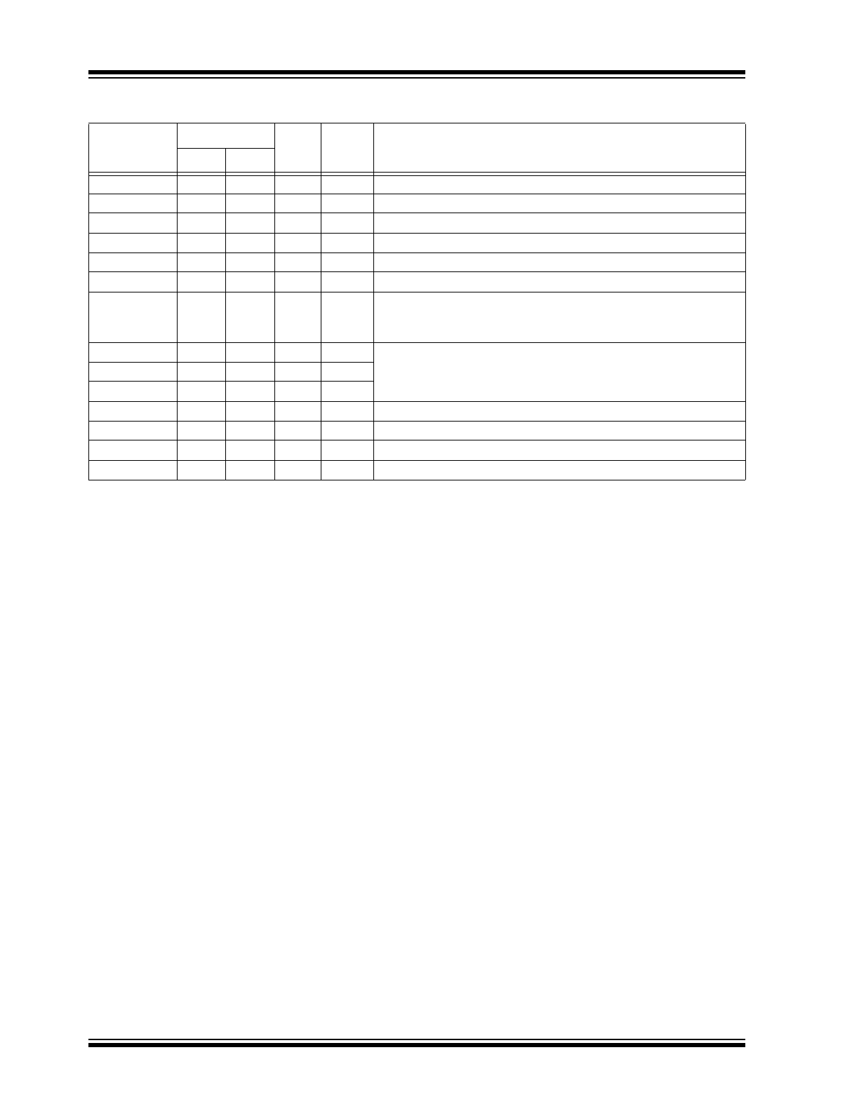
The baud rate for the MCP2120 can be configured
either by the state of three hardware pins (BAUD2,
BAUD1, and BAUD0) or through software selection.
2.4.1.1
Hardware Selection
Three device pins are used to select the baud rate that
the MCP2120 will transmit and receive data. These
pins are called BAUD2, BAUD1, and BAUD0. There is
one pin state (device mode) where the application soft-
ware can specify the baud rate.
Table 2-1
shows the
baud rate configurations.
TABLE 2-1:
HARDWARE BAUD RATE SELECTION VS. FREQUENCY
BAUD2:BAUD0
Frequency (MHz)
Bit Rate
0.6144
(1)
2.000
3.6864
4.9152
7.3728
14.7456
(2)
20.000
(2)
000
800
2604
4800
6400
9600
19200
26042
F
OSC
/ 768
001
1600
5208
9600
12800
19200
38400
52083
F
OSC
/ 384
010
3200
10417
19200
25600
38400
78600
104167
F
OSC
/ 192
011
4800
15625
28800
38400
57600
115200
156250
F
OSC
/ 128
100
9600
31250
57600
78600
115200
230400
312500
F
OSC
/ 64
Note 1: An external clock is recommended for frequencies below 2 MHz.
2: For frequencies above 7.5 MHz, the TXIR pulse width (
parameter IR121
) will be shorter than the minimum
pulse width of 1.6 µs in the IrDA standard specification.
MCP2120
DS21618B-page 6
© 2007 Microchip Technology Inc.
2.4.1.2
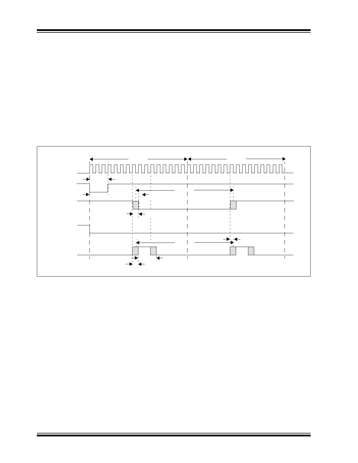
Software Selection
When the BAUD2:BAUD0 pins are configured as ’
111
’
the MCP2120 defaults to a baud rate of F
OSC
/ 768.
To place the MCP2120 into Command Mode, the
MODE pin must be at a low level. When in this mode,
any data that is received by the MCP2120’s UART is
"echoed" back to the controller and no encoding/
decoding occurs. The echoed data will be skewed less
than 1 bit time (see
parameter IR141
). When the
MODE pin goes high, the device is returned to Data
Mode where the encoder/decoder is in operation.
Table 2-2
shows the software hex commands to config-
ure the MCP2120’s baud rate.
The MCP2120 receives data bytes at the existing baud
rate. When the change baud rate command (0x11) is
received, the last valid baud rate value received
becomes the new baud rate. The new baud rate is
effective after the stop bit of the echoed data.
Figure 2-2
shows this sequence.
2.4.2
TRANSMITTING
When the controller sends serial data to the MCP2120,
the baud rates are required to match.
There will be some jitter on the detection of the high to
low edge of the start bit. This jitter will affect the place-
ment of the encoded start bit. All subsequent bits will be
16 BITCLK times later.
2.4.3
RECEIVING
When the controller receives serial data from the
MCP2120, the baud rates are required to match.
There will be some jitter on the detection of the high to
low edge of the start bit. This jitter will affect the place-
ment of the decoded Start bit. All subsequent bits will
be 16 BITCLK times later.
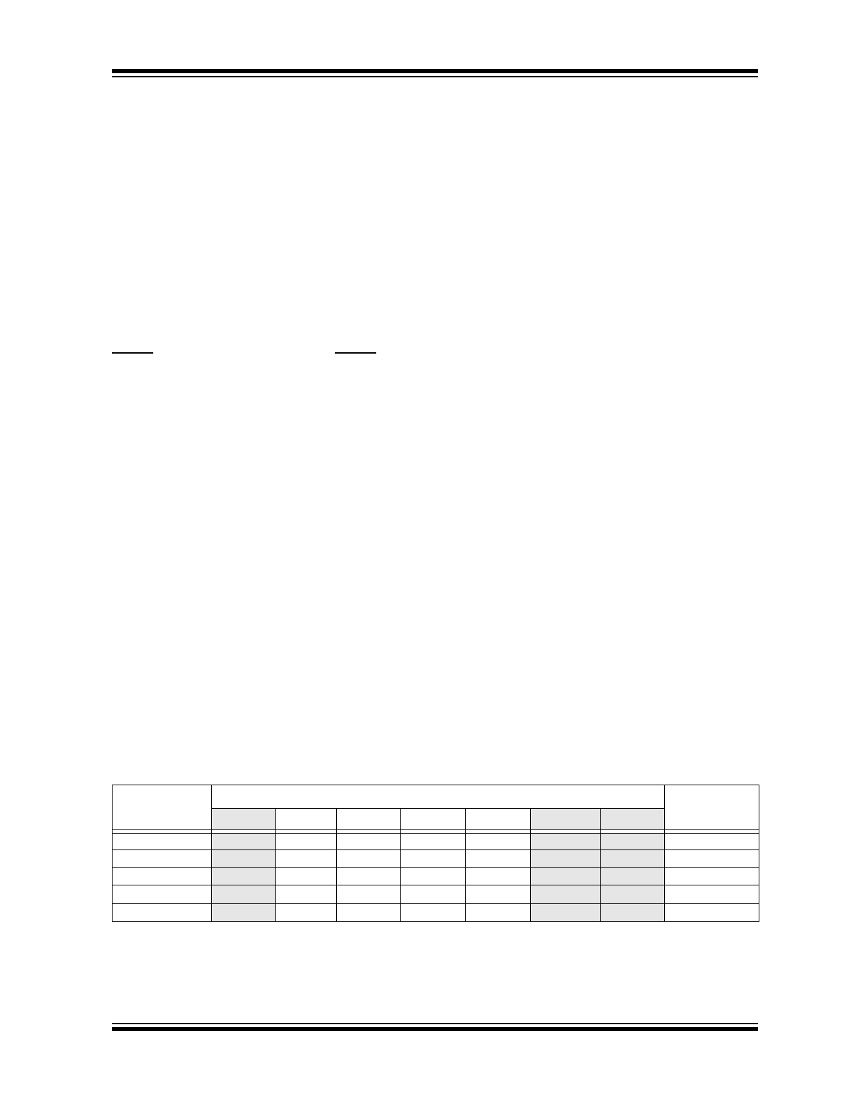
FIGURE 2-1:
Data/Command Mode
Flow
TABLE 2-2:
SOFTWARE BAUD RATE SELECTION VS. FREQUENCY
MODE pin goes low
Data Mode
Command Mode
Controller sends baud
MCP2120 echoes baud
Controller sends 0x11
MCP2120 echoes 0x11
New baud rate
MODE pin goes high
Data Mode
When echoing the Data, once the first bit is
detected, it is echoed back. This means that
the echoed data is skewed no more than 1 bit
time.
The new baud rate can occur once the echoed
stop bit completes.
Hex
Command
(3, 4)
Frequency (MHz)
Bit Rate
0.6144
(1)
2.000
3.6864
4.9152
7.3728
14.7456
(2)
20.000
(2)
0x87
800
2604
4800
6400
9600
19200
26042
F
OSC
/ 768
0x8B
1600
5208
9600
12800
19200
38400
52083
F
OSC
/ 384
0x85
3200
10417
19200
25600
38400
78600
104167
F
OSC
/ 192
0x83
4800
15625
28800
38400
57600
115200
156250
F
OSC
/ 128
0x81
9600
31250
57600
78600
115200
230400
312500
F
OSC
/ 64
Note 1: An external clock is recommended for frequencies below 2 MHz.
2: For frequencies above 7.3728 MHz, the TXIR pulse width (
parameter IR121
) will be shorter than the 1.6 µs
IrDA standard specification.
3: Command 0x11 is used to change to the new baud rate.
4: All other command codes are reserved for possible future use.
© 2007 Microchip Technology Inc.
DS21618B-page 7
MCP2120
2.5
Modulation
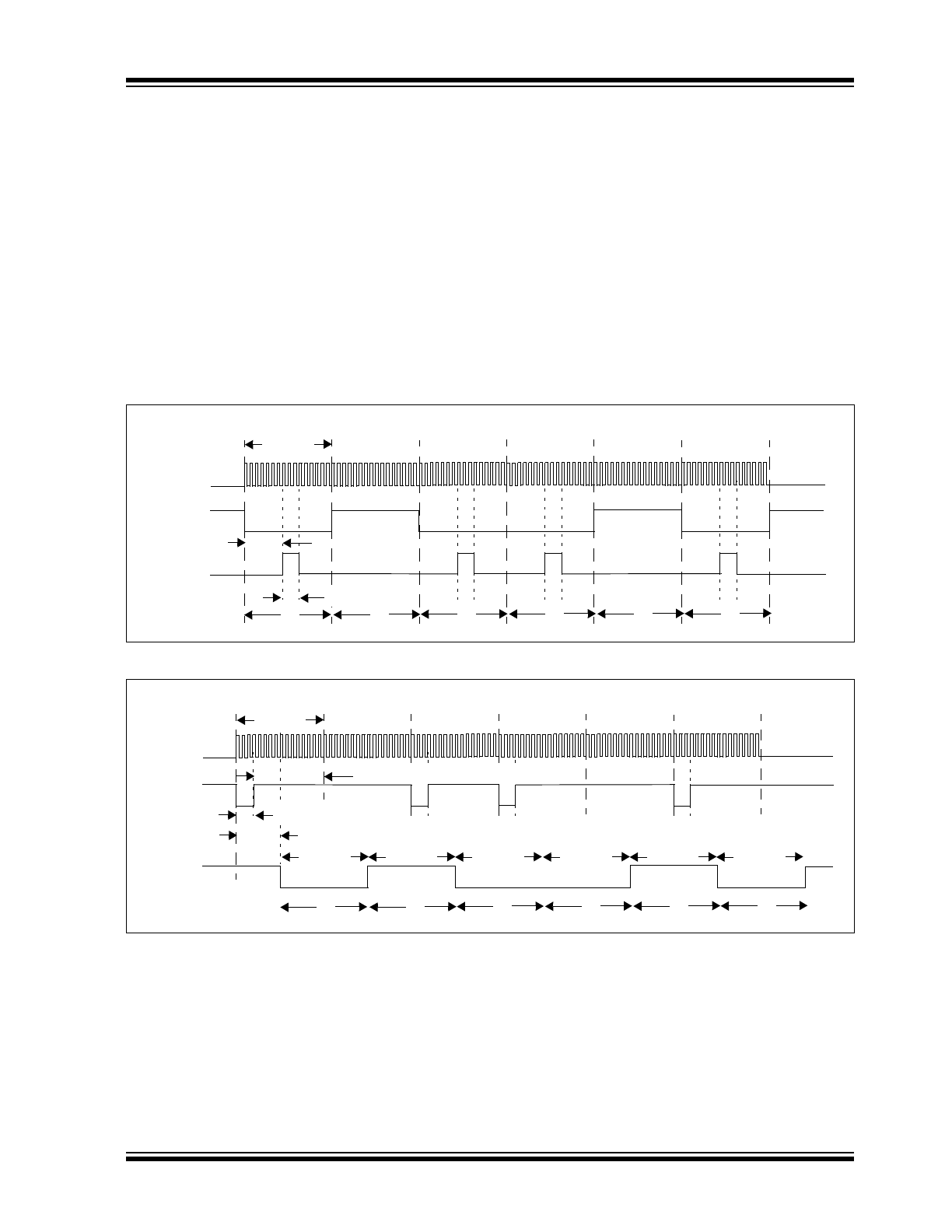
When the UART receives data to be transmitted, the
data needs to be modulated. This modulated signal
drives the IR transceiver module.
Figure 2-2
shows the
encoding of the modulated signal.
Each bit time is comprised of 16-bit clocks. If the value
to be transmitted (as determined by the TX pin) is a
logic low, then the TXIR pin will output a low level for
7-bit clock cycles, a logic high level for 3-bit clock
cycles, and then the remaining 6-bit clock cycles will be
low. If the value to transmit is a logic high, then the
TXIR pin will output a low level for the entire 16-bit clock
cycles.
2.6
Demodulation
The modulated signal from the IR transceiver module
needs to be demodulated to form the received data. As
demodulation occurs, the bit value is placed on the RX
pin in UART format.
Figure 2-3
shows the decoding of
the modulated signal.
Each bit time is comprised of 16 bit clocks. If the value
to be received is a logic low, then the RXIR pin will be
a low level for the first 3-bit clock cycles, and then the
remaining 13-bit clock cycles will be high. If the value to
be received is a logic high, then the RXIR pin will be a
high level for the entire 16-bit clock cycles. The level on
the RX pin will be in the appropriate state for the entire
16 clock cycles.
FIGURE 2-2:
Encoding
FIGURE 2-3:
Decoding
BITCLK
TX
TXIR
0
1
0
0
0
1
16 CLK
Start Bit
Data bit 0
Data bit 1
Data bit 2
Data bit...
7 CLK
12 Tosc
BITCLK
RX
RXIR
0
1
0
0
0
1
≥ 1.6 µs
13 CLK (or
≤ 50.5 µs typical)
16 CLK
16 CLK
16 CLK
16 CLK
16 CLK
16 CLK
16 CLK
8 CLK
Start Bit
Data bit 0
Data bit 1
Data bit 2
Data bit ...
(CLK)
MCP2120
DS21618B-page 8
© 2007 Microchip Technology Inc.
2.7
Encoding/Decoding Jitter and
Offset
Figure 2-4
shows the jitter and offset that is possible on
the RX pin and the TXIR pin.
Jitter is the possible variation of the desired edge.
Offset is the propagation delay of the input signal (RXIR
or TX) to the output signal (RX or TXIR).
The first bit on the output pin (on RX or TXIR) will show
jitter compared to the input pin (RXIR or TX), but all
remaining bits will be a constant distance.
2.8
Minimizing Power
The device can be placed in a low power mode by
disabling the device (holding the EN pin at the low
state). The internal state machine is monitoring this pin
for a low level, and once this is detected the device is
disabled and enters into a low power state.
2.8.1
RETURNING TO OPERATION
When the device is disabled, the device is in a low
power state. When the EN pin is brought to a high level,
the device will return to the operating mode. The device
requires a delay of 1000 T
OSC
before data may be
transmitted or received.
FIGURE 2-4:
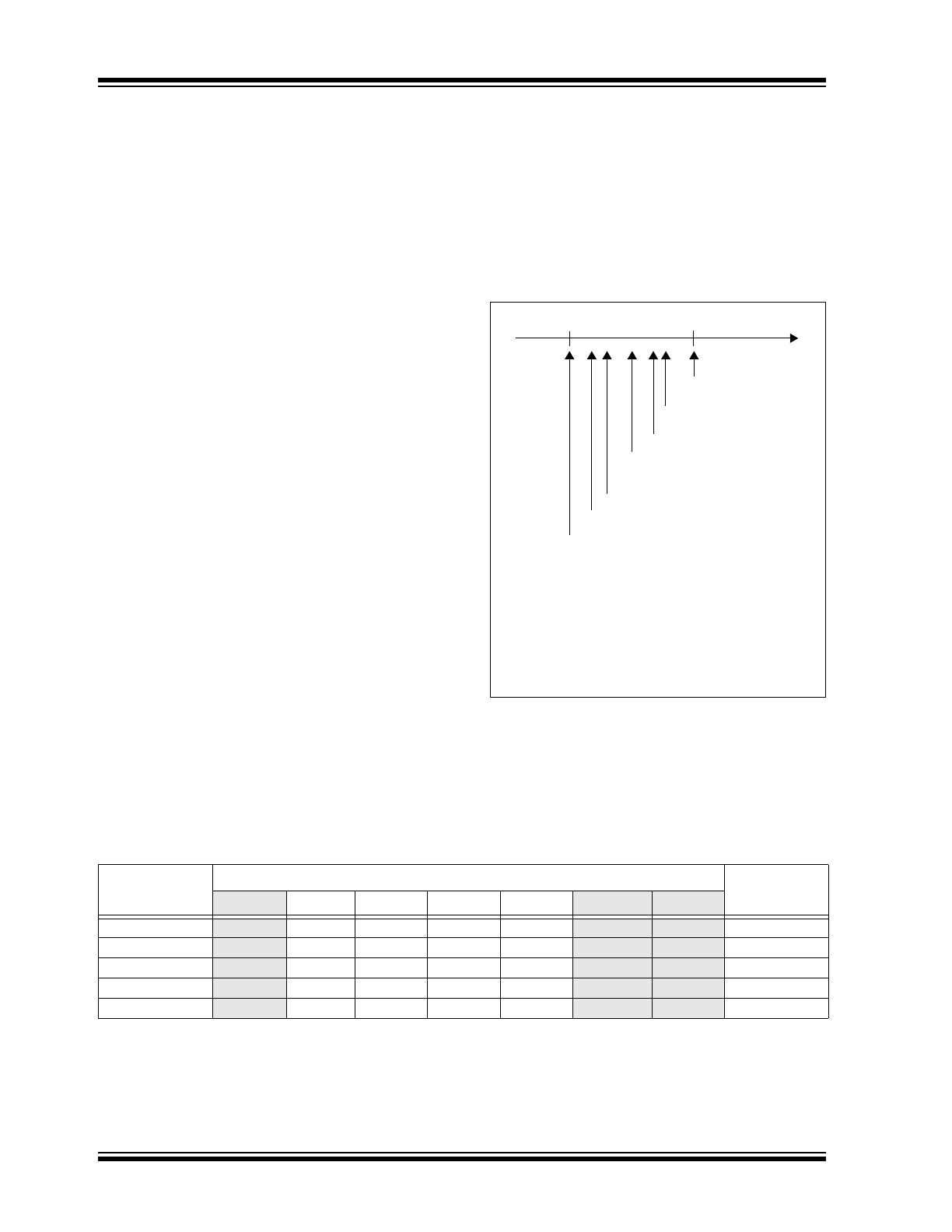
Effects of Jitter and Offset
TX Jitter
3 CLK
BITCLK
RXIR
RX
TX
TXIR
16 CLK
16 CLK
3 CLK
16 CLK
RX Jitter
TX Offset
RX Offset
16 CLK
© 2007 Microchip Technology Inc.
DS21618B-page 9
MCP2120
3.0
DEVELOPMENT TOOLS
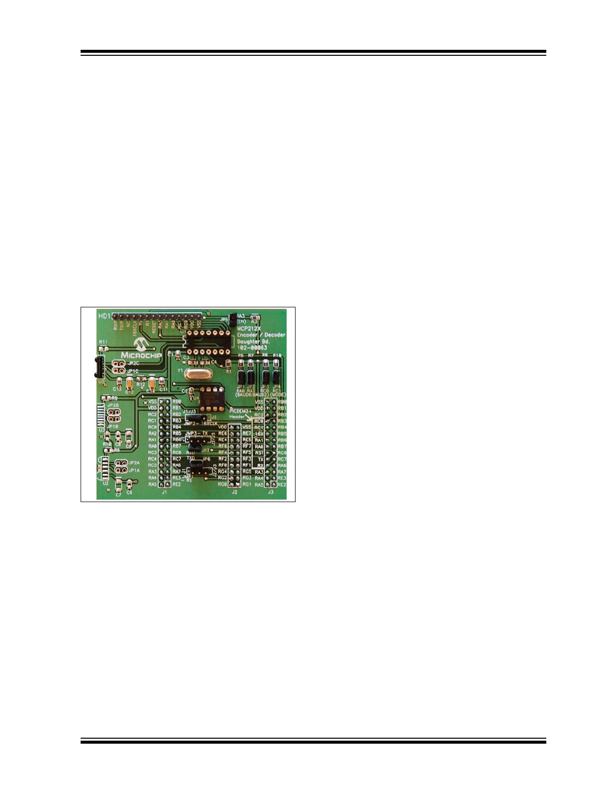
The MCP212X Developer’s Daughter Board is used to
evaluate and demonstrate the MCP2122 or the
MCP2120 IrDA
®
Standard Encoder/Decoder devices.
A header allows the MCP212X Developer’s Daughter
Board to be jumpered easily into systems for
development purposes.
The MCP212X Developer’s Daughter Board is
designed to interface to several of the “new” low cost
PIC
®
Demo Boards. These include the PICDEM HPC
Explorer Demo board, the PICDEM FS USB Demo
board, and the PICDEM LCD Demo board.
When the MCP212X Developer’s Daughter Board is
used in conjunction with the PICDEM HPC Explorer
Demo board, the MCP212x can be connected to either
of the PIC18F8772's two UARTs or the RX and TX sig-
nals can be "crossed" so the MCP212x device can
communicate directly out the PICDEM HPC Explorer
Demo Board's UART (DB-9).
Features:
• 8-pin socket for installation of MCP2122
(installed) and 14-pin socket for installation of
MCP2120
• Three Optical Transceiver circuits (1 installed)
• Headers to interface to low cost PICDEM Demo
Boards, including:
- • PICDEM™ HPC Explorer Demo Board
- • PICDEM™ LCD Demo Board
- • PICDEM™ FS USB Demo Board
- • PICDEM™ 2 Plus Demo Board
• Headers to easily connect to the user’s
embedded system
• Jumpers to select routing of MCP212X signals to
the PICDEM™ Demo Board Headers
• Jumpers to configure the operating mode of the
board
The MCP2120/MCP2150 Developer’s Kit has been
obsoleted but if you have access to one of these kits, it
can be used to demonstrate the operation of the
MCP2120.

MCP2120
DS21618B-page 10
© 2007 Microchip Technology Inc.
NOTES: