
© 2007 Microchip Technology Inc.
Preliminary
DS21894C-page 1
MCP2122
Features
• Pinout compatible with HSDL-7000
• Compliant with IrDA
®
Standard Physical Layer
Specification (version 1.3)
• UART to IrDA Standard Encoder/Decoder
- Interfaces with IrDA Standard Compliant
Transceiver
• Baud Rates:
- Up to IrDA Standard 115.2 Kbaud Operation
• Transmit/Receive Formats (Bit Width) Supported:
- 1.63 µs
• Low-power Mode (2 µA at 1.8V, +125°C)
• Pb-free packaging
CMOS Technology
• Low-voltage operation
• Extended temperature range
• Low power consumption
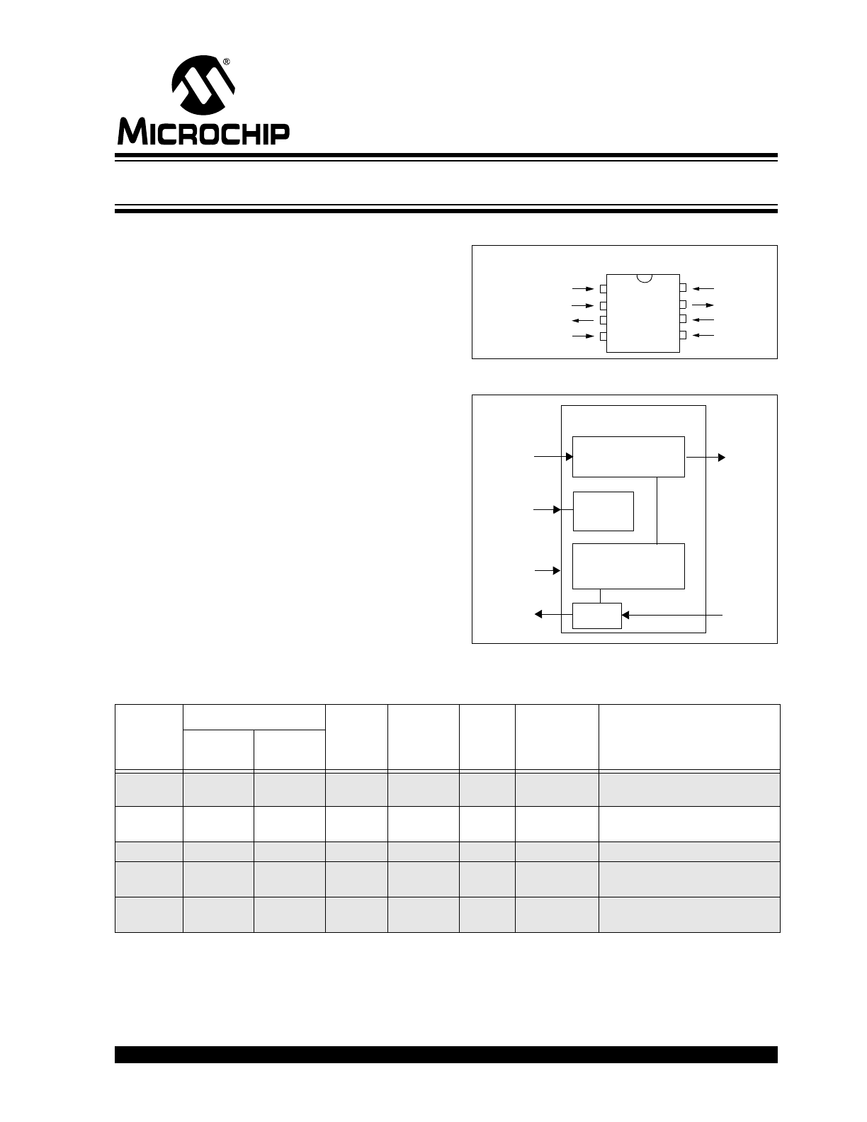
Package Types
Block Diagram
IrDA Family Selection
PDIP, SOIC
MCP2
122
V
SS
16XCLK
RESET
RXIR
TXIR
V
DD
TX
RX
1
2
3
4
8
7
6
5
Encode
Decode
TX
TXIR
RX
RXIR
RESET
MCP2122
Reset
Baud Rate
Generator
Logic
16XCLK
Device
Baud Rate
Encoder
/
Decoder
Protocol
Layer
Handler
Clock
Source
Host UART
Baud Rate
Selection
Comment
Host
UART
IR
MCP2120 2400 -
312,500
(1)
2400 -
312,500
(1)
Yes
No
XTAL
HW/SW
MCP2122 2400 -
115,200
(1)
2400 -
115,200
(1)
Yes
No
16XCLK By 16XCLK Extended Temperature Range
(-40°C to +125°C)
MCP2140 9600
9600
Yes
IrCOMM
(3)
XTAL
None - Fixed
MCP2150 9600 -
115,200
(2)
9600 -
115,200
(2)
Yes
IrCOMM
(3)
XTAL
HW
Host UART easily interfaces to
a PC’s serial port (DTE)
MCP2155 9600 -
115,200
(2)
9600 -
115,200
(2)
Yes
IrCOMM
(3)
XTAL
HW
Host UART easily interfaces to
a modem’s serial port (DCE)
Note 1: The host UART and the IR operate at the same baud rates.
2: The host UART and IR baud rates operate independent of each other.
3: Supports the 9-wire “cooked” service class of the IrCOMM Application Layer Protocol.
Infrared Encoder/Decoder

MCP2122
DS21894C-page 2
Preliminary
© 2007 Microchip Technology Inc.
NOTES:
© 2007 Microchip Technology Inc.
Preliminary
DS21894C-page 3
MCP2122
1.0
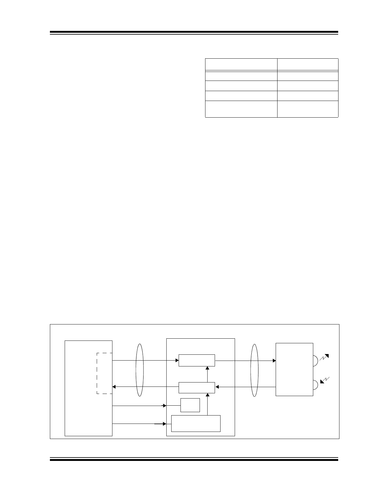
DEVICE OVERVIEW
The MCP2122 is a stand-alone IrDA standard encoder/
decoder device that is pinout-compatible with the
Agilent
®
HSDL-7000 encoder/decoder.
The MCP2122 has two interfaces: the host UART
interface and the IR interface (see
Figure 1-1
). The host
UART interfaces to the UART of the Host Controller.
The Host Controller is the device in the embedded
system that transmits and receives the data. The IR
interface connects to an infrared (IR) optical transceiver
circuit that converts electrical pulses into IR light
(encode) and converts IR light into electrical pulses
(decode). This IR optical transceiver circuit could be
either a standard infrared optical transceiver (such as a
Vishay
®
TFDU 4300) or it could be implemented with
discrete components. For additional information, please
refer to AN243, “Fundamentals of the Infrared Physical
Layer” (DS00243).
When the Host Controller transmits the UART format
data, the MCP2122 receives this UART data and
encodes (modulates) it bit by bit. This encoded data is
then output as electrical pulses to the IR transceiver.
The IR transceiver will then convert these electrical
pulses to IR light pulses.
The IR transceiver also receives IR light pulses (data),
which are outputted as electrical pulses. The MCP2122
decodes (demodulates) these electrical pulses, with
the data then being transmitted by the MCP2122
UART. This modulation/demodulation method is
performed in accordance with the IrDA standard.
Table 1-1
shows an overview of some of the device
features.
Figure 1-1
shows a typical application block
diagram.
Table 1-2
shows the pin definitions of the
MCP2122 during normal operation.
TABLE 1-1:
MCP2122 FEATURES
OVERVIEW
Infrared Technology Features:
• Universal standard for connecting portable
computing devices
• Effortless implementation
• Economical alternative to other connectivity
solutions
• Reliable, high-speed connection
• Safe to use in any environment; can even be used
during air travel
• Eliminates the hassle of cables
• Allows PCs and non-PCs to communicate with
each other
• Enhances mobility by allowing users to easily
connect
1.1
Applications
Some applications where an IR interface (MCP2122)
could be used include:
• Data-Logging/Data Exchange
• System Setup
• System Diagnostic Read Out
• Manufacturing Configuration
• Host Controller Firmware Updates
• System Control
FIGURE 1-1:
SYSTEM BLOCK DIAGRAM
Features
MCP2122
Serial Communications:
UART, IR
Baud Rate Selection:
16XCLK
Low-power Mode:
Yes
Packages:
8-pin PDIP
8-pin SOIC
Encode
Decode
TX
TXIR
RX
RXIR
RESET
MCP2122
PIC
®
SO
SI
TFDU 4300
UAR
T
TXD
RXD
Reset
Logic
Clock
Logic
16XCLK
Clock
Host UART
Interface
IR
Interface
Host Controller
Protocol Handler
Optical
Transceiver
(I/O)
MCU
MCP2122
DS21894C-page 4
Preliminary
© 2007 Microchip Technology Inc.
TABLE 1-2:
PIN DESCRIPTION
Pin Name
Pin Number
Pin
Type
Buffer
Type
PDIP
SOIC
Description
16XCLK
1
1
I
ST
16x external clock source input
TX
2
2
I
ST
Asynchronous receive from Host Controller UART
RX
3
3
O
—
Asynchronous transmit to Host Controller UART
V
SS
4
4
—
P
Ground reference for logic and I/O pins
RESET
5
5
I
ST
Resets the Device
H = Normal Operation
L = Device in Reset
RXIR
6
6
I
ST
Asynchronous receive from infrared transceiver
TXIR
7
7
O
—
Asynchronous transmit to infrared transceiver
V
DD
8
8
—
P
Positive supply for logic and I/O pins
Legend:
ST = Schmitt Trigger input with CMOS levels
I = Input
P = Power
O = Output
© 2007 Microchip Technology Inc.
Preliminary
DS21894C-page 5
MCP2122
2.0
DEVICE OPERATION
The MCP2122 is a low-cost infrared encoder/decoder.
The baud rate is the same for the host UART and IR
interfaces and is determined by the frequency of the
16XCLK signal, with a maximum baud rate of
115.2 Kbaud.
The MCP2122 is made up of these functional modules:
• Clock Driver (16XCLK)
• Reset
• IR Encoder/Decoder
- IrDA Standard Encoder
- IrDA Standard Decoder
The 16XCLK circuit allows a clock input to provide the
device clock.
The Reset circuit supports an external reset signal.
The IR Encoder logic takes a data bit and converts it to
the IrDA standard signal according to the IrDA standard
Physical Layer specification, while the IR Decoder
logic takes the IrDA standard signal and converts it to
8-bit data bytes.
2.1
Power-up
As the device is powered up, there will be a voltage
range in which the device will not operate properly. The
device should be reset once it has entered the normal
operating range (from an out-of-voltage condition). The
RESET pin may then be forced high.
Other device operating parameters (such as frequency,
temperature, etc.) must also be within their operating
ranges when the device exits reset. Otherwise, the
device may not function as desired.
2.2
Device Reset
The MCP2122 is forced into the known state (RESET)
when the RESET pin is in the low state. Once the
RESET pin is brought to a high state, the device begins
normal operation (if the device operating parameters
are met).
Table 2-1
shows the states of the output pins
while the device is in reset (RESET = Low).
Table 2-2
shows the state of the output pins once the device exits
reset, RESET = L
→H (device in Normal Operation
mode).
The MCP2122 has a RESET noise filter in the RESET
input signal path. The filter will detect and ignore small
pulses.
Using the RESET pin to enter a low-power state is
discussed in Section 2.9 “Minimizing Power”.
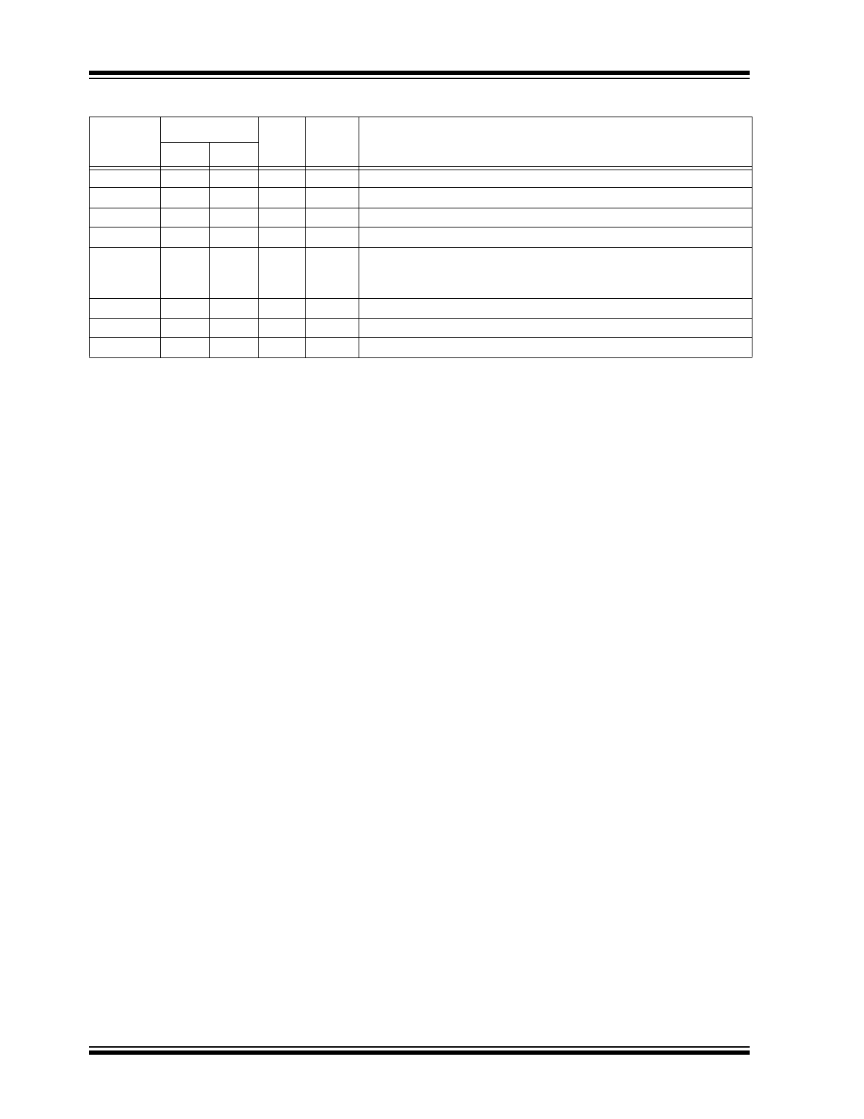
TABLE 2-1:
DEFAULT OUTPUT PIN
STATES IN DEVICE RESET
TABLE 2-2:
DEFAULT OUTPUT PIN
STATES AFTER DEVICE
RESET (RESET = L
→H)
2.3
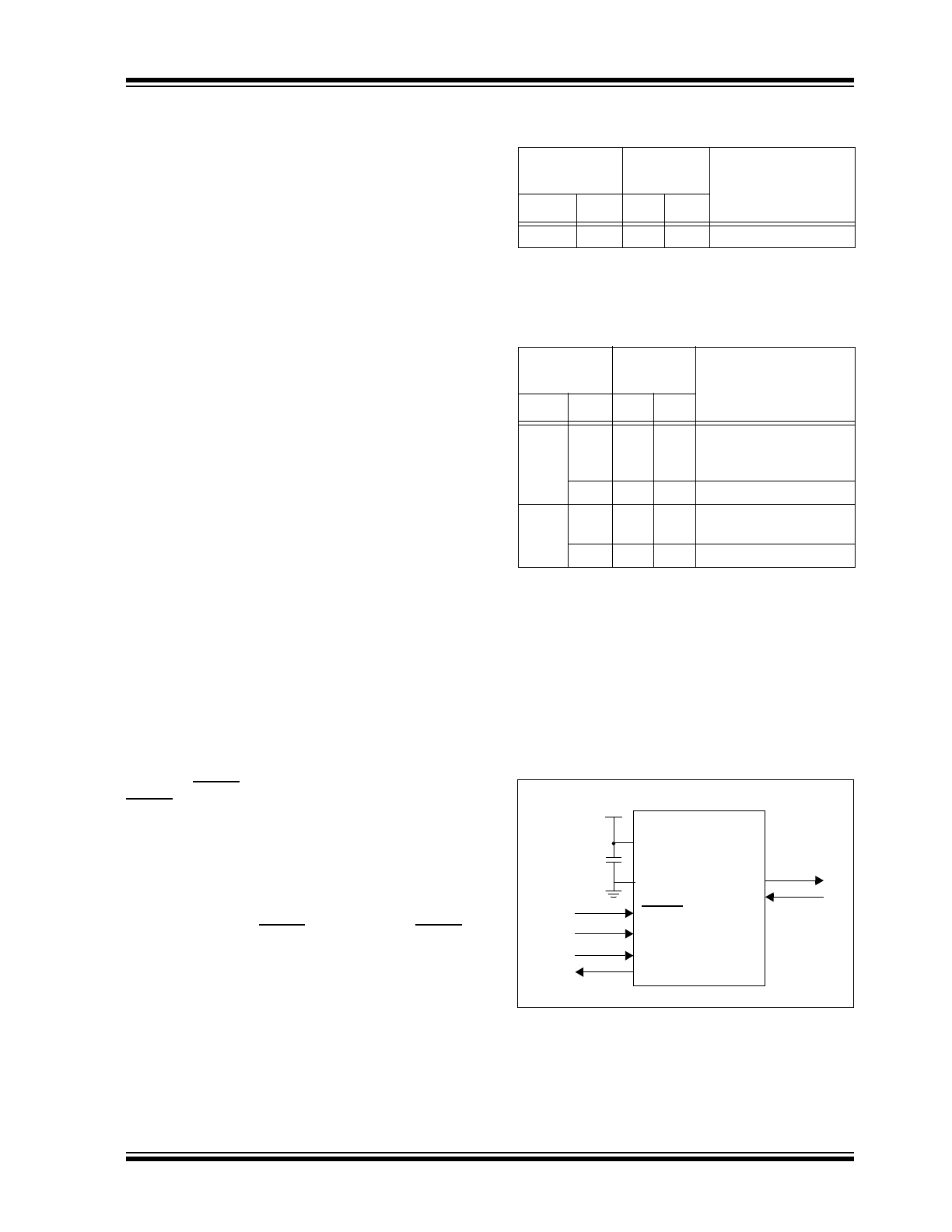
Decoupling
It is highly recommended that the MCP2122 have a
decoupling capacitor (C
BYP
). A 0.01 µF capacitor is
recommended as a starting value, but an evaluation of
the best value for your circuit/layout should be
performed. Place this decoupling capacitor (C
BYP
) as
close to the MCP2122 as possible (see
Figure 2-1
).
FIGURE 2-1:
DEVICE DECOUPLING
Input Pin
Output Pin
State
Comments
Name
State
RX
TXIR
RESET
L
H
L
Device in Reset mode
Input Pin
Output Pin
State
Comments
Name State
RX
TXIR
TX
L
—
L
→H
→L
After 7 - 8 16XCLK
pulses, the TXIR pin
will pulse high.
H
—
L
RXIR
L
H
→L
—
After 4 16XCLK pulses,
RX = L.
H
H
—
V
DD
(bypass
capacitor)
MCP2122
V
DD
RESET
V
SS
16XCLK
TX
RX
TXIR
RXIR
C
BYP
MCP2122
DS21894C-page 6
Preliminary
© 2007 Microchip Technology Inc.
2.3.1
BROWN-OUTS
Some applications may subject the MCP2122 to a
brown-out condition. Good design practice requires
that when a system is in brown-out, the system should
be in reset to ensure that the system is in a known
state when the system exits the brown-out. This
brown-out circuitry is external to the MCP2122.
2.3.1.1
External Brown-Out Reset Circuits
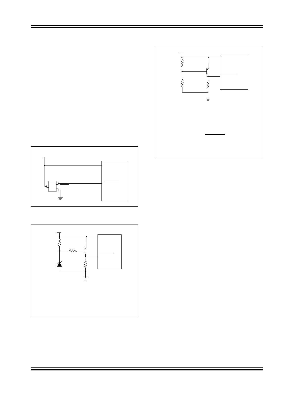
Figure 2-2
shows a circuit for external brown-out
protection using the TCM809 device.
Figure 2-3
and
Figure 2-4
illustrate two examples of
external circuitry that may be implemented. Each
option needs to be evaluated to determine if they
satisfy the requirements of the application.
FIGURE 2-2:
EXTERNAL BROWN-OUT
PROTECTION USING THE
TCM809
FIGURE 2-3:
EXTERNAL BROWN-OUT
PROTECTION CIRCUIT 1
FIGURE 2-4:
EXTERNAL BROWN-OUT
PROTECTION CIRCUIT 2
V
SS
RST
TCM809
V
DD
MCP2122
V
DD
RESET
Note 1: Resistors should be adjusted for the
characteristics of the transistor.
2: This circuit will activate reset when
V
DD
goes below (Vz + 0.7V),
where Vz = Zener voltage.
V
DD
33 k
Ω
10 k
Ω
40 k
Ω
V
DD
RESET
MCP2122
Q1
R2
40 k
Ω
V
DD
RESET
MCP2122
R1
Q1
V
DD
Note 1: This circuit is less expensive, but
less accurate. Transistor Q1 turns
off when V
DD
is below a certain level
such that:
2: Resistors should be adjusted for the
characteristics of the transistor.
V
DD
•
R1
R1 + R2
= 0.7V
© 2007 Microchip Technology Inc.
Preliminary
DS21894C-page 7
MCP2122
2.4
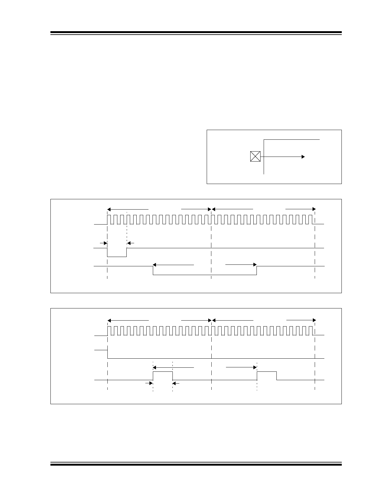
16XCLK (Bit Clock)
The MCP2122 requires an external clock source to
operate. The 16XCLK pin is the device clock input (see
Figure 2-5
) and is independent of the host UART
interface or the IR interface. The 16XCLK determines
all timing during device operation. It is the edge of the
16XCLK pin that causes activity to occur.
The 16XCLK signal can also be referred to as a bit
clock (BITCLK). There are 16 BITCLKs for each bit
time. The BITCLKs are used for the generation of the
Start bit, the eight data bits and the Stop bit.
When the embedded system could be receiving IR
communication, the MCP2122 is required to have the
16XCLK signal clocking at the expected frequency,
with minimal variation in that frequency. Between data
bytes (Stop bit to Start bit), the 16XCLK frequency can
be changed. This may occur in systems where the Host
Controller is implementing one of the IrDA standard
application layer protocols (such as IrObex).
When the embedded system does not want to receive
IR communications, the 16XCLK clock can be disabled
(static). This will reduce the power consumption of the
system.
Figure 2-6
shows the relationship of the 16XCLK signal
to the RXIR input, which then determines the RX output
signal.
Figure 2-7
shows the relationship of the
16XCLK signal to the TX input, which then determines
the TXIR output signal. For device timing information,
refer to Section 4.0 “Electrical Characteristics”.
FIGURE 2-5:
DEVICE CLOCK SOURCE
FIGURE 2-6:
16XCLK AND RX/RXIR
FIGURE 2-7:
16XCLK AND TX/TXIR
MCP2122
16XCLK
16XCLK
RXIR
RX
16 16XCLK
16 16XCLK
≤ 3 CLK
16 16XCLK
Bit A
Bit B
(input)
(output)
(input)
3 CLK (
≤ ~ 4 µs)
16XCLK
TX
TXIR
16 16XCLK
16 16XCLK
16 16XCLK
Bit A
Bit B
(input)
(output)
(input)
MCP2122
DS21894C-page 8
Preliminary
© 2007 Microchip Technology Inc.
2.4.1
BAUD RATE
The baud rate for the MCP2122 is determined by the
frequency of the 16XCLK signal.
Equation 2-1
demonstrates how to calculate the 16XCLK frequency
based on the desired baud rate.
Table 2-3
shows some
common baud rates and the corresponding 16XCLK
frequency.
EQUATION 2-1:
16XCLK FREQUENCY
TABLE 2-3:
COMMON BAUD RATE/
16XCLK FREQUENCY
2.5
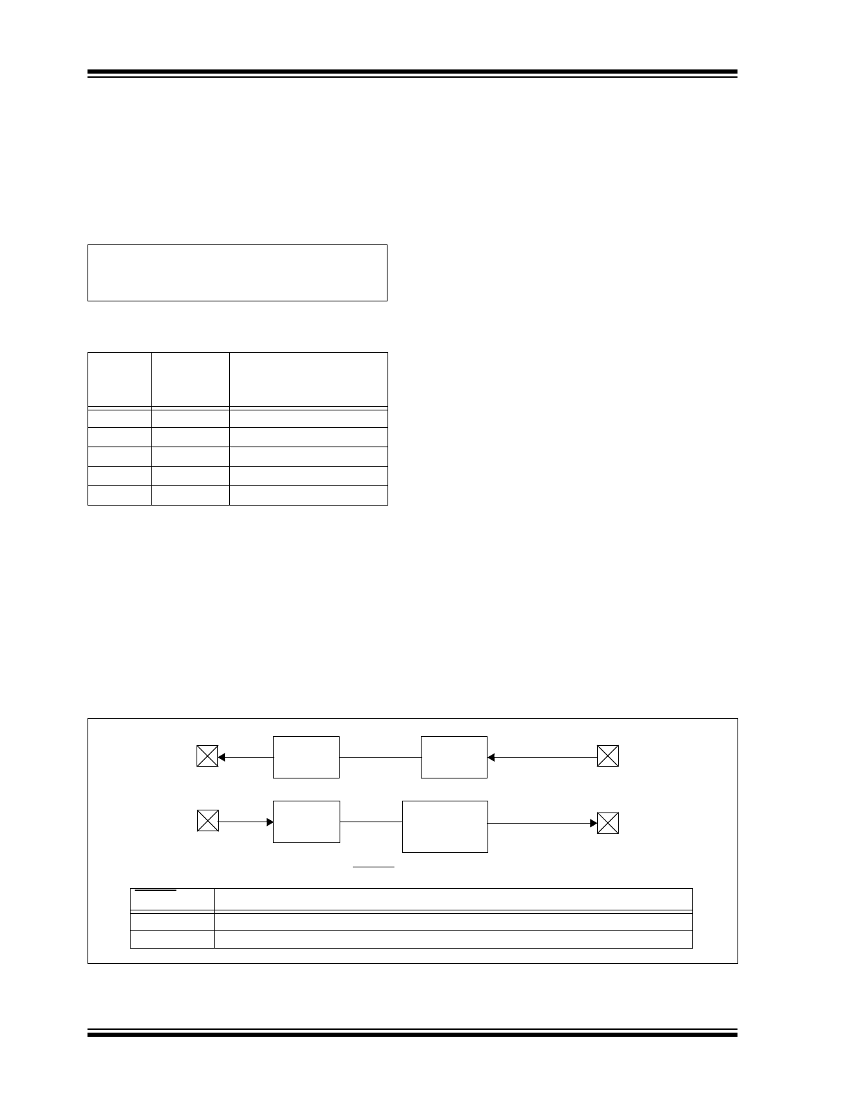
Encoder/Decoder
The IR encoder/decoder is made up of two major
components. They are:
• IR Decoder
• IR Encoder
The encoder receives UART data (bit by bit) and
outputs a data bit in the IrDA standard bit format.
Figure 2-8
shows a functional block diagram of the
encoder.
The decoder receives IrDA standard data (bit by bit)
and outputs data in UART data bit format.
Figure 2-8
shows a functional block diagram of the decoder.
The encoder/decoder has two interfaces. They are:
• Host UART interface
• IR interface
2.5.1
ENCODING (MODULATION)
Each bit time is comprised of 16 bit clocks. If the value
to be transmitted (as determined by the TX pin) is a
logic-low, the TXIR pin will output a low level for 7-bit
clock cycles, a logic-high level for 3-bit clock (with a
maximum high-time of about 4 µs) cycles, with the
remaining time (6-bit clock cycles or more) being low. If
the value to transmit is a logic-high, the TXIR pin will
output a low level for the entire 16 bit clock cycle.
2.5.2
DECODING (DEMODULATION)
Each bit time is comprised of 16 bit clocks. If the value
to be received is a logic-low, the RXIR pin will be a low
level for the first 3-bit clock cycle (or a minimum of
1.6 µs), with the remaining time (13-bit clock cycles)
being high. If the value to be received is a logic-high,
the RXIR pin will be a high level for the entire 16-bit
clock cycle. The level on the RX pin will be in the
appropriate state for an entire 16-bit clock cycle.
FIGURE 2-8:
MCP2122 RECEIVE DETECT TO ENCODER/DECODER BLOCK DIAGRAM
Baud
Rate
16XCLK
Frequency
(F
16
XCLK
)
Comment
9600
153,600
19,200
307,200
38,400
614,400
57,600
921,600
115,200
1,843,200
F
16XCLK
16 (Desired Baud Rate)
•
=
TXIR
Glitch
Filter
Decode
RX
RXIR
Pulse Width
Limiter
Encode
TX
The following table shows the state on the RESET pin and how this effects the operation of the TXIR pin.
RESET State
Comment
V
IH
TXIR output encoded value of TX pin
V
IL
TXIR is forced low
(~ 4 µs)
© 2007 Microchip Technology Inc.
Preliminary
DS21894C-page 9
MCP2122
2.5.3
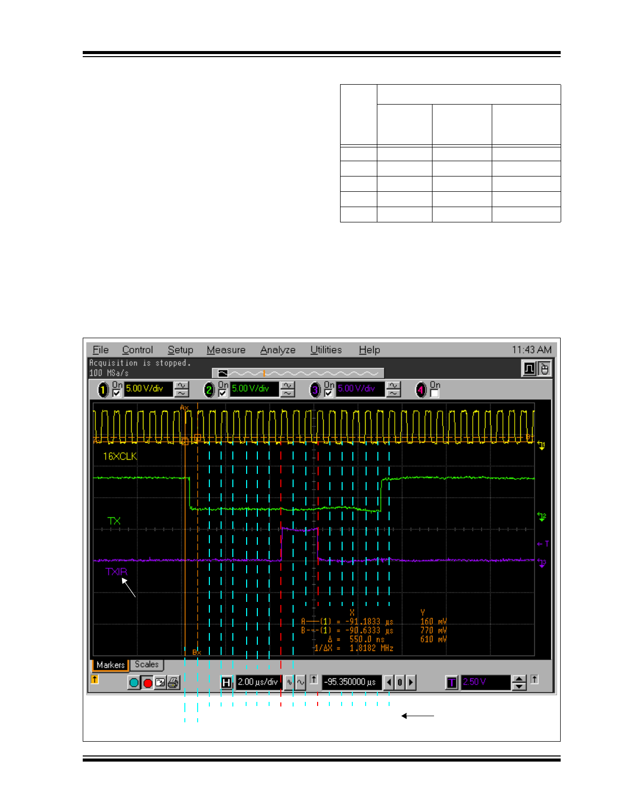
ENCODING AND SCREEN
CAPTURES
Table 2-4
shows the TXIR pin high-time at different
common baud rates. The internal TXIR pulse-width
high-time limiter is a feature that minimizes the system
current consumption at lower baud rates. The IrDA
standard specification requires that optical receiver cir-
cuitry detect pulses as narrow as 1.41 µs (1.63 µs is
the typical time at 115200 baud). Therefore, the time
that the TXIR pin is high after this valid detection is
additional current that is driven by the emitter LED. The
MCP2122 will force the TXIR pin low once the pulse-
width limiter has timed out.
Figure 2-9
shows the
MCP2122 16XCLK, TX and TXIR waveforms at
115200 baud for a single TX low bit. In this case, the
TXIR is high for three 16XCLK pulses. In
Figure 2-10
,
the MCP2122 is at 9600 baud for a single TX low bit. In
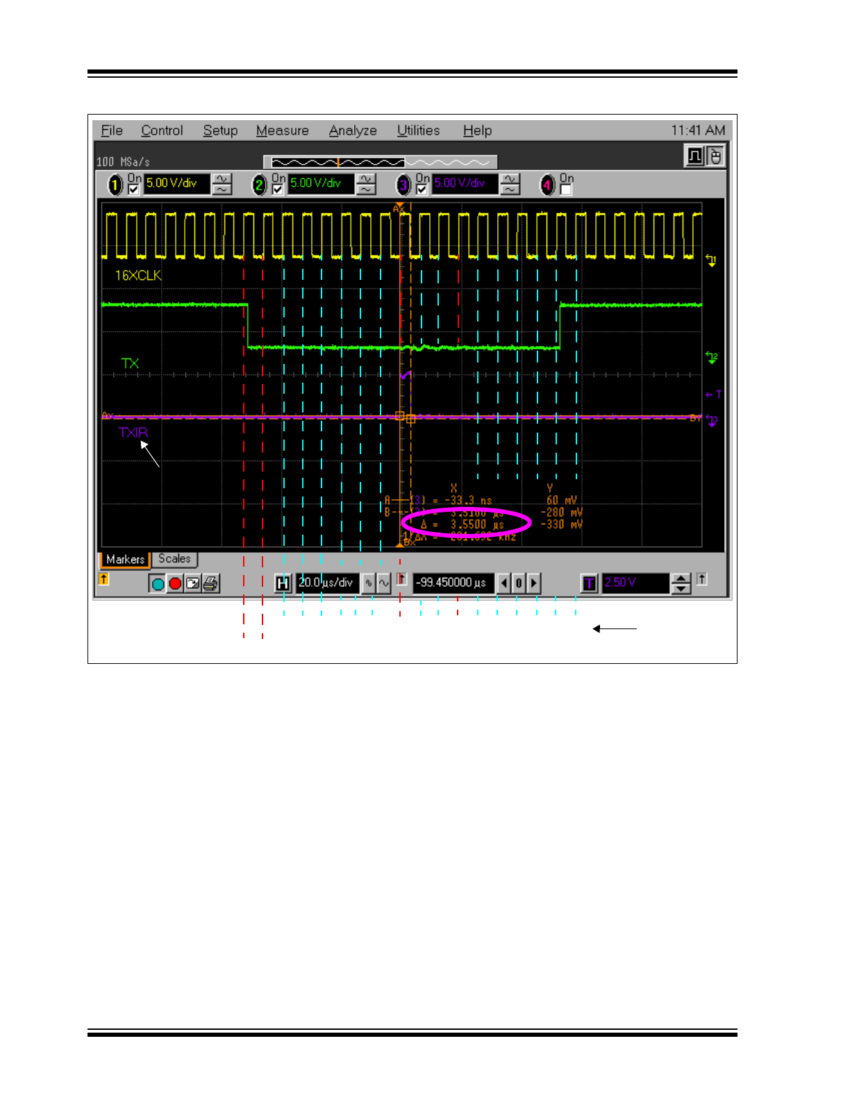
this case, the TXIR is high for 3.55 µs (determined by
pulse-width limiter circuit).
TABLE 2-4:
TXIR HIGH PULSE WIDTH
FIGURE 2-9:
MCP2122 AT 115200 BAUD WAVEFORM
Baud
Rate
TXIR Pulse Width
3xT
16
XCLK
Circuit
Pulse-width
Limiter
(2)
Circuit
Actual Pulse
Width
9600
19.53 µs
(1)
4.00 µs
4.00 µs
(3)
19200
9.77 µs
(1)
4.00 µs
4.00 µs
(3)
38400
4.88 µs
(1)
4.00 µs
4.00 µs
(3)
57600
3.26 µs
4.00 µs
3.26 µs
115200
1.63 µs
4.00 µs
1.63 µs
Note 1: The pulse-width limiter on the TXIR pin
saves system current for this baud rate.
2: This TXIR pulse width time is a design
target and is not tested. Actual times may
be greater than, or less than, this value.
3: This time (determined by the pulse-width
limiter circuit) is device dependent.
1 2 3 4 5 6 7 8 9 10 11 12 13 14 15 16
Jitter of the TX input relative to the 16XCLK and TXIR
16XCLK Pulse
A B
TXIR
MCP2122
DS21894C-page 10
Preliminary
© 2007 Microchip Technology Inc.
FIGURE 2-10:
MCP2122 AT 9600 BAUD WAVEFORM
1 2 3 4 5 6
7 8 9 10 11 12 13 14 15 16
16XCLK Pulse
Jitter of the TX input relative to the 16XCLK and TXIR
A B
TXIR