

AT24C16D
I²C-Compatible (2-Wire) Serial EEPROM 16-Kbit (2,048 x 8)
Features
•
Low-Voltage Operation:
–
Vcc = 1.7V to 3.6V
•
Internally Organized as 2,048 x 8 (16K)
•
I
2
C-Compatible (2-Wire) Serial Interface:
–
100 kHz Standard mode, 1.7V to 3.6V
–
400 kHz Fast mode, 1.7V to 3.6V
–
1 MHz Fast Mode Plus (FM+), 2.5V to 3.6V
•
Schmitt Triggers, Filtered Inputs for Noise Suppression
•
Bidirectional Data Transfer Protocol
•
Write-Protect Pin for Full Array Hardware Data Protection (except WLCSP)
•
Ultra Low Active Current (1 mA maximum) and Standby Current (0.8 μA maximum)
•
16-Byte Page Write Mode:
–
Partial page writes allowed
•
Random and Sequential Read Modes
•
Self-Timed Write Cycle within 5 ms Maximum
•
ESD Protection > 4,000V
•
High Reliability:
–
Endurance: 1,000,000 write cycles
–
Data retention: 100 years
•
Green Package Options (Lead-free/Halide-free/RoHS compliant)
•
Die Sale Options: Wafer Form and Tape and Reel Available
Packages
•
8-lead PDIP
(
1
)
, 8-lead SOIC, 5-lead SOT23, 8-lead TSSOP, 8-pad UDFN, 8-ball VFBGA, and 4-ball
WLCSP
Note:
1.
Contact Microchip Sales for the availability of this package.
©
2017 Microchip Technology Inc.
Datasheet
DS20005858A-page 1

Table of Contents
Features.......................................................................................................................... 1
Packages.........................................................................................................................1
1. Package Types.......................................................................................................... 4
2. Pin Descriptions.........................................................................................................5
2.1.
Ground......................................................................................................................................... 5
2.2.
Serial Data (SDA).........................................................................................................................5
2.3.
Serial Clock (SCL)........................................................................................................................5
2.4.
Write-Protect................................................................................................................................ 6
2.5.
Device Power Supply................................................................................................................... 6
3. Description.................................................................................................................7
3.1.
System Configuration Using 2-Wire Serial EEPROMs.................................................................7
3.2.
Block Diagram.............................................................................................................................. 8
4. Electrical Characteristics........................................................................................... 9
4.1.
Absolute Maximum Ratings..........................................................................................................9
4.2.
DC and AC Operating Range.......................................................................................................9
4.3.
DC Characteristics....................................................................................................................... 9
4.4.
AC Characteristics......................................................................................................................10
4.5.
Electrical Specifications..............................................................................................................12
5. Device Operation and Communication....................................................................14
5.1.
Clock and Data Transition Requirements...................................................................................14
5.2.
Start and Stop Conditions.......................................................................................................... 14
5.3.
Acknowledge and No-Acknowledge...........................................................................................15
5.4.
Standby Mode............................................................................................................................ 15
5.5.
Software Reset...........................................................................................................................16
6. Memory Organization.............................................................................................. 17
6.1.
Device Addressing..................................................................................................................... 17
7. Write Operations......................................................................................................18
7.1.
Byte Write...................................................................................................................................18
7.2.
Page Write..................................................................................................................................18
7.3.
Acknowledge Polling.................................................................................................................. 19
7.4.
Write Cycle Timing..................................................................................................................... 19
7.5.
Write Protection..........................................................................................................................20
8. Read Operations..................................................................................................... 21
8.1.
Current Address Read................................................................................................................21
8.2.
Random Read............................................................................................................................ 21
8.3.
Sequential Read.........................................................................................................................22
AT24C16D
©
2017 Microchip Technology Inc.
Datasheet
DS20005858A-page 2

9. Device Default Condition from Microchip................................................................ 23
10. Packaging Information.............................................................................................24
10.1. Package Marking Information.....................................................................................................24
11. Revision History.......................................................................................................32
The Microchip Web Site................................................................................................ 33
Customer Change Notification Service..........................................................................33
Customer Support......................................................................................................... 33
Product Identification System........................................................................................34
Microchip Devices Code Protection Feature................................................................. 34
Legal Notice...................................................................................................................35
Trademarks................................................................................................................... 35
Quality Management System Certified by DNV.............................................................36
Worldwide Sales and Service........................................................................................37
AT24C16D
©
2017 Microchip Technology Inc.
Datasheet
DS20005858A-page 3
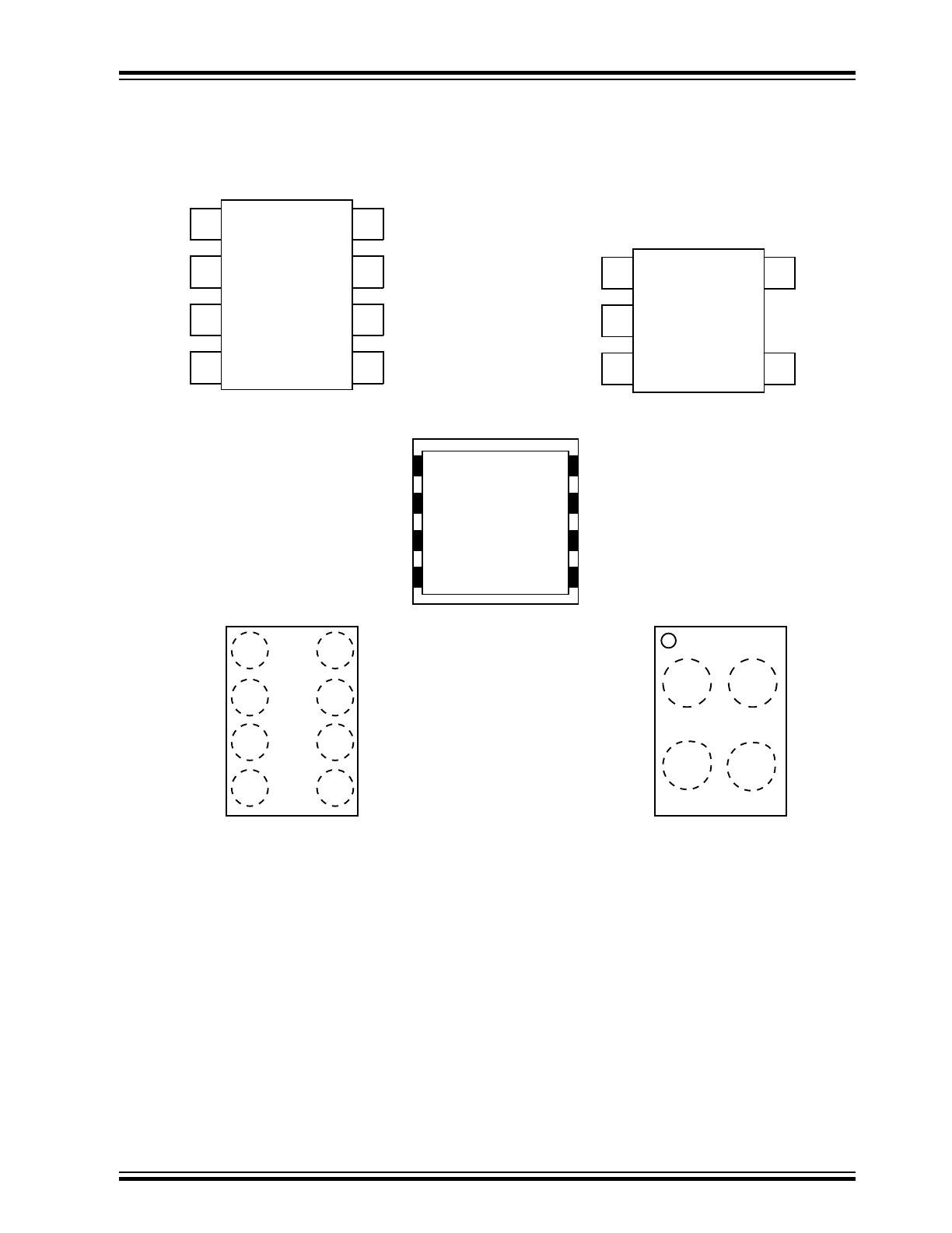
1.
Package Types
NC
NC
NC
GND
Vcc
WP
SCL
SDA
8-pad UDFN
(Top View)
8-lead PDIP/SOIC/TSSOP
(Top View)
NC
1
2
3
4
8
7
6
5
NC
NC
GND
Vcc
WP
SCL
SDA
1
2
3
4
8
7
6
5
NC
NC
NC
GND
Vcc
WP
SCL
SDA
8-ball VFBGA
(Top View)
Vcc
SCL
4-ball WLCSP
(1)
(Top View)
GND
SDA
5-lead SOT23
(Top View)
SCL
1
2
3
5
4
GND
SDA
WP
Vcc
1
2
3
4
5
6
7
8
A1
A2
B1
B2
Note:
1.
Since the WLCSP has no WP pin, the write protection feature is not offered on the WLCSP.
AT24C16D
©
2017 Microchip Technology Inc.
Datasheet
DS20005858A-page 4

2.
Pin Descriptions
The descriptions of the pins are listed in
Table 2-1
.
Table 2-1. Pin Function Table
Name
8-lead
PDIP
8-lead
SOIC
8-lead
TSSOP
5-lead
SOT23
8-pad
UDFN
(
1
)
8-ball
VFBGA
4-ball
WLCSP
Function
NC
1
1
1
-
1
1
-
No Connect
NC
2
2
2
-
2
2
-
No Connect
NC
3
3
3
-
3
3
-
No Connect
GND
4
4
4
2
4
4
A2
Ground
SDA
5
5
5
3
5
5
B2
Serial Data
SCL
6
6
6
1
6
6
B1
Serial Clock
WP
(
2
)
7
7
7
5
7
7
-
Write-Protect
V
CC
8
8
8
4
8
8
A1
Device Power
Supply
Note:
1.
The exposed pad on the UDFN package can be connected to GND or left floating.
2.
If the WP pin is not driven, it is internally pulled down to GND. In order to operate in a wide variety
of application environments, the pull-down mechanism is intentionally designed to be somewhat
strong. Once these pins are biased above the CMOS input buffer’s trip point (~0.5 x V
CC
), the pull
‑down mechanism disengages. Microchip recommends connecting these pins to a known state
whenever possible. Since the WLCSP has no WP pin, the write protection feature is not offered on
the WLCSP.
2.1
Ground
The ground reference for the power supply. GND should be connected to the system ground.
2.2
Serial Data (SDA)
The SDA pin is an open-drain bidirectional input/output pin used to serially transfer data to and from the
device. The SDA pin must be pulled-high using an external pull-up resistor (not to exceed 10 kΩ in value)
and may be wire-ORed with any number of other open-drain or open-collector pins from other devices on
the same bus.
2.3
Serial Clock (SCL)
The SCL pin is used to provide a clock to the device and to control the flow of data to and from the
device. Command and input data present on the SDA pin is always latched in on the rising edge of SCL,
while output data on the SDA pin is clocked out on the falling edge of SCL. The SCL pin must either be
forced high when the serial bus is idle or pulled high using an external pull-up resistor.
AT24C16D
©
2017 Microchip Technology Inc.
Datasheet
DS20005858A-page 5

2.4
Write-Protect
Connecting the WP pin to GND will ensure normal write operations. When the WP pin is connected to
V
CC
, all write operations to the memory are inhibited. Refer to
Note 2
for the behavior of the pin when not
connected.
2.5
Device Power Supply
The V
CC
pin is used to supply the source voltage to the device. Operations at invalid V
CC
voltages may
produce spurious results and should not be attempted.
AT24C16D
©
2017 Microchip Technology Inc.
Datasheet
DS20005858A-page 6
3.
Description
The AT24C16D provides 16,384 bits of Serial Electrically Erasable and Programmable Read-Only
Memory (EEPROM) organized as 2,048 words of 8 bits each. This device is optimized for use in many
industrial and commercial applications where low-power and low-voltage operations are essential. The
device is available in space-saving 8-lead SOIC, 8-lead TSSOP, 8-pad UDFN, 8-lead PDIP
(
1
)
, 5-lead
SOT23, 8-ball VFBGA and 4-ball WLCSP packages. The entire family of packages operates from 1.7V to
3.6V.
Note:
1.
Contact Microchip Sales for the availability of this package.
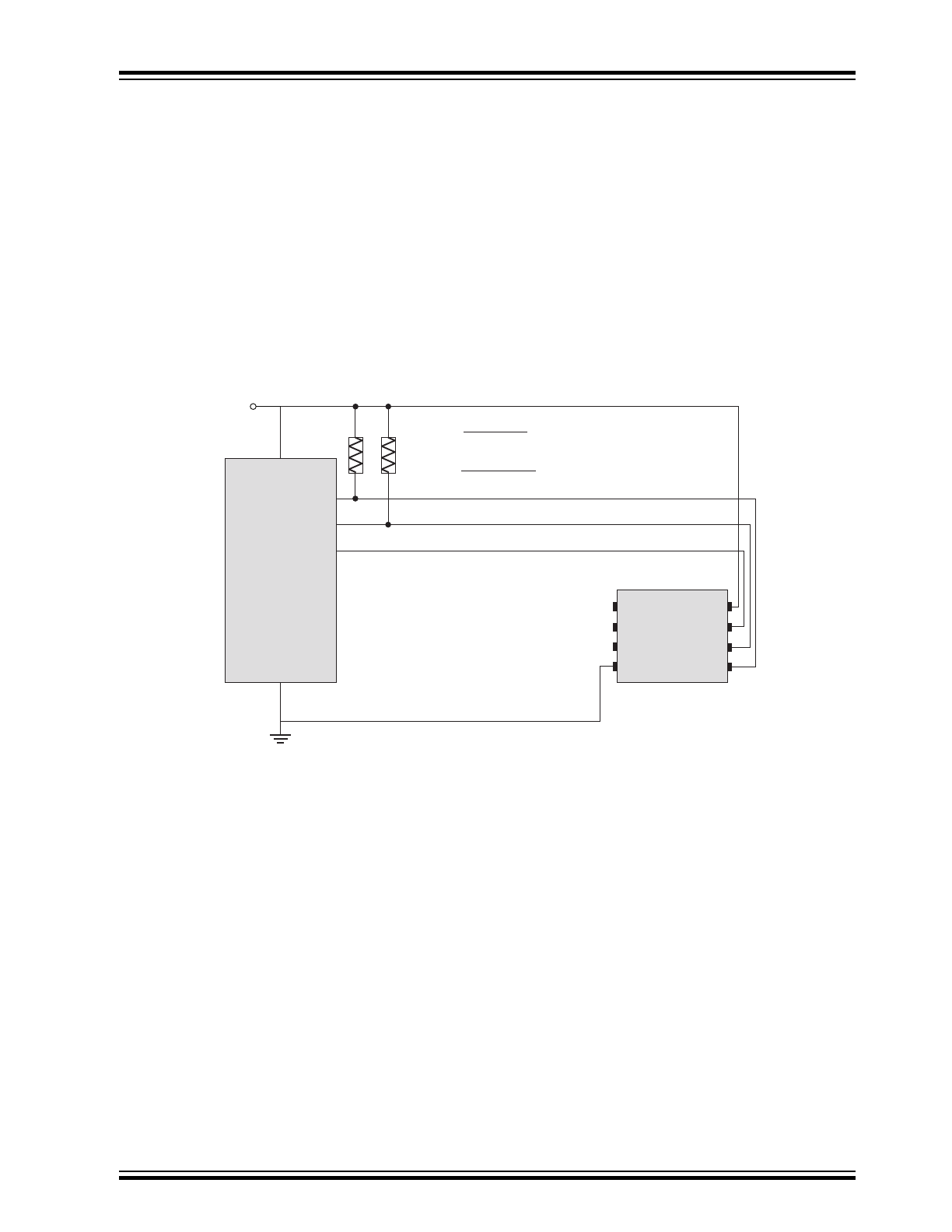
3.1
System Configuration Using 2-Wire Serial EEPROMs
I
2
C Bus Master:
Microcontroller
V
CC
GND
SCL
SDA
WP
R
PUP(max) =
t
R(max)
0.8473 x C
L
R
PUP(min) =
V
CC
- V
OL(max)
I
OL
Slave
AT24CXXX
V
CC
WP
SDA
SCL
NC
NC
NC
GND
V
CC
AT24C16D
©
2017 Microchip Technology Inc.
Datasheet
DS20005858A-page 7
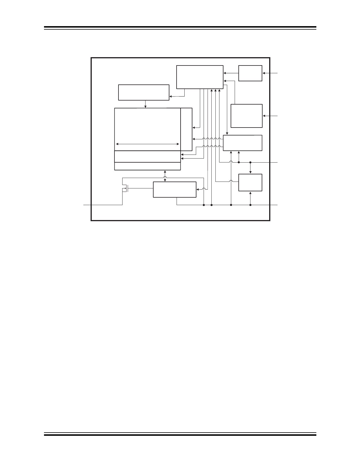
3.2
Block Diagram
1 page
Start
Stop
Detector
GND
Memory
System Control
Module
High-Voltage
Generation Circuit
Data & ACK
Input/Output Control
Address Register
and Counter
Write
Protection
Control
D
OUT
D
IN
V
CC
WP
SCL
SDA
POR
Generator
EEPROM Array
Column Decoder
Row Decoder
Data Register
AT24C16D
©
2017 Microchip Technology Inc.
Datasheet
DS20005858A-page 8

4.
Electrical Characteristics
4.1
Absolute Maximum Ratings
Temperature under bias
-55°C to +125°C
Storage temperature
-65°C to +150°C
Supply voltage with respect to ground
-0.5V to +4.10V
Voltage on any pin with respect to ground
–0.6V to Vcc + 0.5V
DC output current
5.0 mA
ESD protection
>4 kV
Note: Stresses above those listed under “Absolute Maximum Ratings” may cause permanent damage to
the device. This is a stress rating only and functional operation of the device at those or any other
conditions above those indicated in the operation listings of this specification is not implied. Exposure
above maximum rating conditions for extended periods may affect device reliability.
4.2
DC and AC Operating Range
Table 4-1. DC and AC Operating Range
AT24C16D
Operating Temperature (Case)
Industrial Temperature Range
-40°C to +85°C
V
CC
Power Supply
Low Voltage Grade
1.7V to 3.6V
4.3
DC Characteristics
Table 4-2. DC Characteristics
Parameter
Symbol
Minimum
Typical
(
1
)
Maximum
Units
Test Conditions
Supply
Voltage
V
CC
1.7
—
3.6
V
Supply
Current,
Read
I
CC1
—
0.08
0.3
mA
V
CC
= 1.8V
(
2
)
, Read at
400 kHz
—
0.15
0.5
mA
V
CC
= 3.6V, Read at 1 MHz
Supply
Current,
Write
I
CC2
—
0.20
1.0
mA
V
CC
= 3.6V, Write at 1 MHz
Standby
Current
I
SB
—
0.08
0.4
μA
V
CC
= 1.8V
(
2
)
, V
IN
= V
CC
or
GND
—
0.10
0.8
μA
V
CC
= 3.6V, V
IN
= V
CC
or
GND
AT24C16D
©
2017 Microchip Technology Inc.
Datasheet
DS20005858A-page 9

Parameter
Symbol
Minimum
Typical
(
1
)
Maximum
Units
Test Conditions
Input
Leakage
Current
I
LI
—
0.10
3.0
μA
V
IN
= V
CC
or GND
Ouput
Leakage
Current
I
LO
—
0.05
3.0
μA
V
OUT
= V
CC
or GND
Input Low
Level
V
IL
-0.6
—
V
CC
x 0.3
V
Note 2
Input High
Level
V
IH
V
CC
x 0.7
—
V
CC
+ 0.5
V
Note 2
Output Low
Level
V
OL1
—
—
0.2
V
V
CC
= 1.8V, I
OL
= 0.15 mA
Output Low
Level
V
OL2
—
—
0.4
V
V
CC
= 3.0V, I
OL
= 2.1 mA
Note:
1.
Typical values characterized at T
A
= +25°C unless otherwise noted.
2.
This parameter is characterized but is not 100% tested in production.
4.4
AC Characteristics
Table 4-3. AC Characteristics
Parameter
Symbol
Standard Mode
Fast Mode
Fast Mode Plus
Units
V
CC
= 1.7V to 3.6V
V
CC
= 1.7V to 3.6V
V
CC
= 2.5V to 3.6V
Min.
Max.
Min.
Max.
Min.
Max.
Clock
Frequency,
SCL
f
SCL
—
100
—
400
—
1000
kHz
Clock Pulse
Width Low
t
LOW
4,700
—
1,300
—
500
—
ns
Clock Pulse
Width High
t
HIGH
4,000
—
600
—
400
—
ns
Input Filter
Spike
Suppression
(SCL,SDA)
(
1
)
t
I
—
100
—
100
—
100
ns
Clock Low to
Data Out Valid
t
AA
—
4,500
—
900
—
450
ns
Bus Free Time
between Stop
and Start
(
1
)
t
BUF
4,700
—
1,300
—
500
—
ns
Start Hold
Time
t
HD.STA
4,000
—
600
—
250
—
ns
AT24C16D
©
2017 Microchip Technology Inc.
Datasheet
DS20005858A-page 10