

2014 Microchip Technology Inc.
DS20005296B-page 1
HV9989
Features
• Three out-of-phase constant-current boost
converters
• Current loop closed, with sub-microsecond PWM-
dimming pulses, supports PWM dimming >20 kHz
• Internal 40V linear regulator
• External clock input
• External individual reference inputs
• Individual PWM dimming inputs
• Programmable slope compensation
• +0.2A/-0.4A gate drivers
• Independent short circuit protection with hiccup
for each channel
• Latching output open-circuit protection
Applications
• LCD panel back-lighting
Description
HV9989 is a three-channel peak current mode PWM
controller designed to drive single switch converters in
a constant-output current mode. It can be used for driv-
ing either RGB LEDs or multiple channels of white
LEDs.
HV9989 features a proprietary PWM-dimming control
algorithm that achieves a dimming pulse of a few hun-
dred nanoseconds from a Continuous-Conduction
Mode (CCM) or Discontinuous-Conduction Mode
(DCM) boost converter, while maintaining the instanta-
neous LED constant current determined by the external
reference voltage input. This feature permits a dimming
frequency outside of the audible range, and can also
yield a wide dimming ratio in excess of 10,000:1 at low
dimming frequency. Each of the three channels fea-
tures individual PWM-dimming and reference voltage
inputs.
The switching frequencies of the three converters are
controlled by an external clock signal, such that the
channels operate at a switching frequency of 1/12th the
external clock frequency, and are positioned 120
°
out-
of-phase to reduce the input current ripple.
HV9989 provides a full protection feature set, including
output-short and open-circuit protection, for each indi-
vidual channel that is independent from the other chan-
nels.
HV9989 is powered by a built-in 40V linear regulator.
Three-Channel CCM/DCM Boost LED Driver
with Sub-Microsecond PWM Dimming

HV9989
DS20005296B-page 2
2014 Microchip Technology Inc.
TO OUR VALUED CUSTOMERS
It is our intention to provide our valued customers with the best documentation possible to ensure successful use of your Microchip
products. To this end, we will continue to improve our publications to better suit your needs. Our publications will be refined and
enhanced as new volumes and updates are introduced.
If you have any questions or comments regarding this publication, please contact the Marketing Communications Department via
E-mail at
docerrors@microchip.com
. We welcome your feedback.
Most Current Data Sheet
To obtain the most up-to-date version of this data sheet, please register at our Worldwide Web site at:
http://www.microchip.com
You can determine the version of a data sheet by examining its literature number found on the bottom outside corner of any page.
The last character of the literature number is the version number, (e.g., DS30000000A is version A of document DS30000000).
Errata
An errata sheet, describing minor operational differences from the data sheet and recommended workarounds, may exist for current
devices. As device/documentation issues become known to us, we will publish an errata sheet. The errata will specify the revision
of silicon and revision of document to which it applies.
To determine if an errata sheet exists for a particular device, please check with one of the following:
• Microchip’s Worldwide Web site;
http://www.microchip.com
• Your local Microchip sales office (see last page)
When contacting a sales office, please specify which device, revision of silicon and data sheet (include literature number) you are
using.
Customer Notification System
Register on our web site at
www.microchip.com
to receive the most current information on all of our products.
2014 Microchip Technology Inc.
DS20005296B-page 3
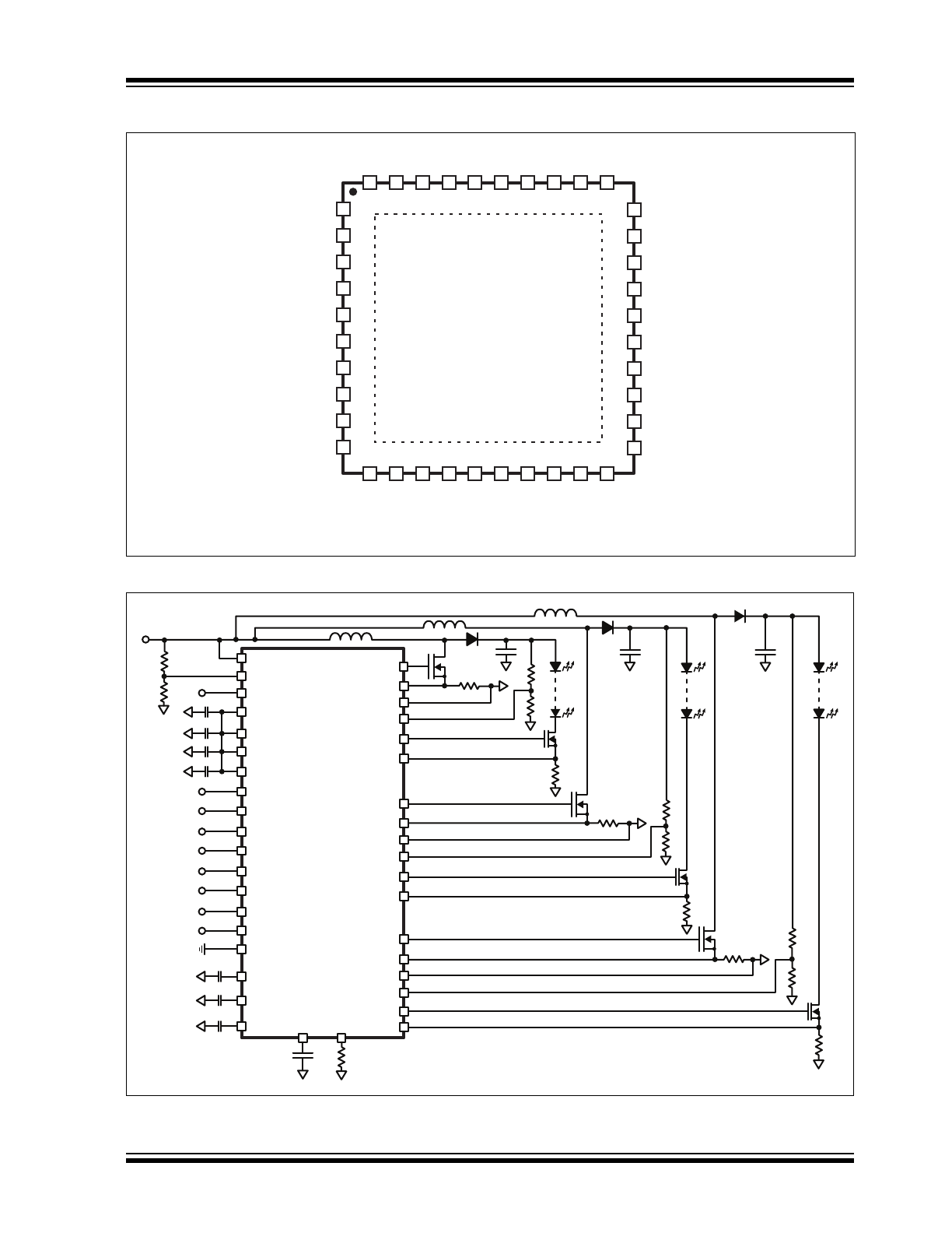
HV9989
Pin Diagram
Typical Application Circuit
40-Lead QFN
VDD3
FLT3
CS3
COMP3
FDBK3
REF3
OVP3
CLK
FLG
VIN_SNS
GND
1
10
11
20
40
30
21
31
VDD1
FLT1
CS1
COMP1
FDBK1
REF1
OVP1
VIN
VDD
EN
GND
COMP2
REF2
OVP2
SKIP
SC
PWMD1
PWMD2
PWMD3
NC
GATE1
GND1
FDBK2
CS2
FLT2
GATE2
GND2
VDD2
GND3
GATE3
GATE1
CS1
GND1
OVP1
FLT1
FDBK1
GATE2
CS2
GND2
OVP2
FLT2
FDBK2
GATE3
CS3
GND3
OVP3
FLT3
FDBK3
VIN
VIN_SNS
FLG
VDD
VDD1
VDD2
VDD3
PWMD1
PWMD2
PWMD3
REF1
REF2
REF3
EN
CLK
GND
COMP1
COMP2
COMP3
SKIP
SC
HV9989
HV9989
DS20005296B-page 4
2014 Microchip Technology Inc.
1.0
ELECTRICAL
CHARACTERISTICS
ABSOLUTE MAXIMUM RATINGS †
V
IN
to GND........................................................ -0.5V to +45V
V
DD
to GND, V
DD
1-3 to GND..........................--0.3V to +10V
All other pins to GND .............................-0.3V to (V
DD
+ 0.3V)
Operating temperature ....................................-40°C to +85°C
Storage temperature .....................................-65°C to +150°C
Continuous power dissipation (T
A
= +25°C).............4000 mW
† Notice: Stresses above those listed under “Absolute Maxi-
mum Ratings” may cause permanent damage to the device.
This is a stress rating only and functional operation of the
device at those or any other conditions, above those indi-
cated in the operational listings of this specification, is not
implied. Exposure to maximum rating conditions for extended
periods may affect device reliability.
1.1
ELECTRICAL SPECIFICATIONS
TABLE 1-1:
ELECTRICAL CHARACTERISTICS (SHEET 1 OF 3)
1
Symbol
Parameter
Note
Min
Typ
Max
Units Conditions
Input
VINDC
Input DC supply voltage
1
10
—
40
V
DC input voltage
IINSD
Shut-down mode supply
current
1
—
—
500
μA
EN = 0.8V
IIN
Supply current
—
—
—
4.5
mA
EN ≥ 2.0V; PWMD1 = PWMD2
= PWMD3 = GND
Internal Regulator
VDD
Internally regulated voltage
1
7.0
—
8.1
V
VIN= 11V; EN = GND;
External IDD = 30mA
∆ VDD
Load regulation
—
—
—
80
mV
VIN= 11V; EN = GND;
External IDD(A) = 10mA,
IDD(B) = 30mA
∆ VDD = VDD(A) - VDD(B)
UVLO
VDD under voltage lockout
threshold
—
5.9
—
6.4
V
VDD falling
UVLOHYST
VDD under voltage hystere-
sis
—
-
500
-
mV
VDD rising
PWM Dimming (PWMD1, PWMD2 and PWMD3)
VPWMD(lo) PWMD input low voltage
1
—
—
0.8
V
—
VPWMD(hi) PWMD input high voltage
1
2.0
—
—
V
—
RPWMD
PWMD pull down resistor
—
80
—
160
kΩ
VPWMD = 5.0V
Td
Delay time to PWMD latch
2
50
—
150
ns
—
TDP
DMAX inhibit delay
2
—
400
—
ns
—
Note 1:
Applies over the full operating ambient temperature range of 0°C < T
A
< +85°C.
2:
For design guidance only.
2014 Microchip Technology Inc.
DS20005296B-page 5
HV9989
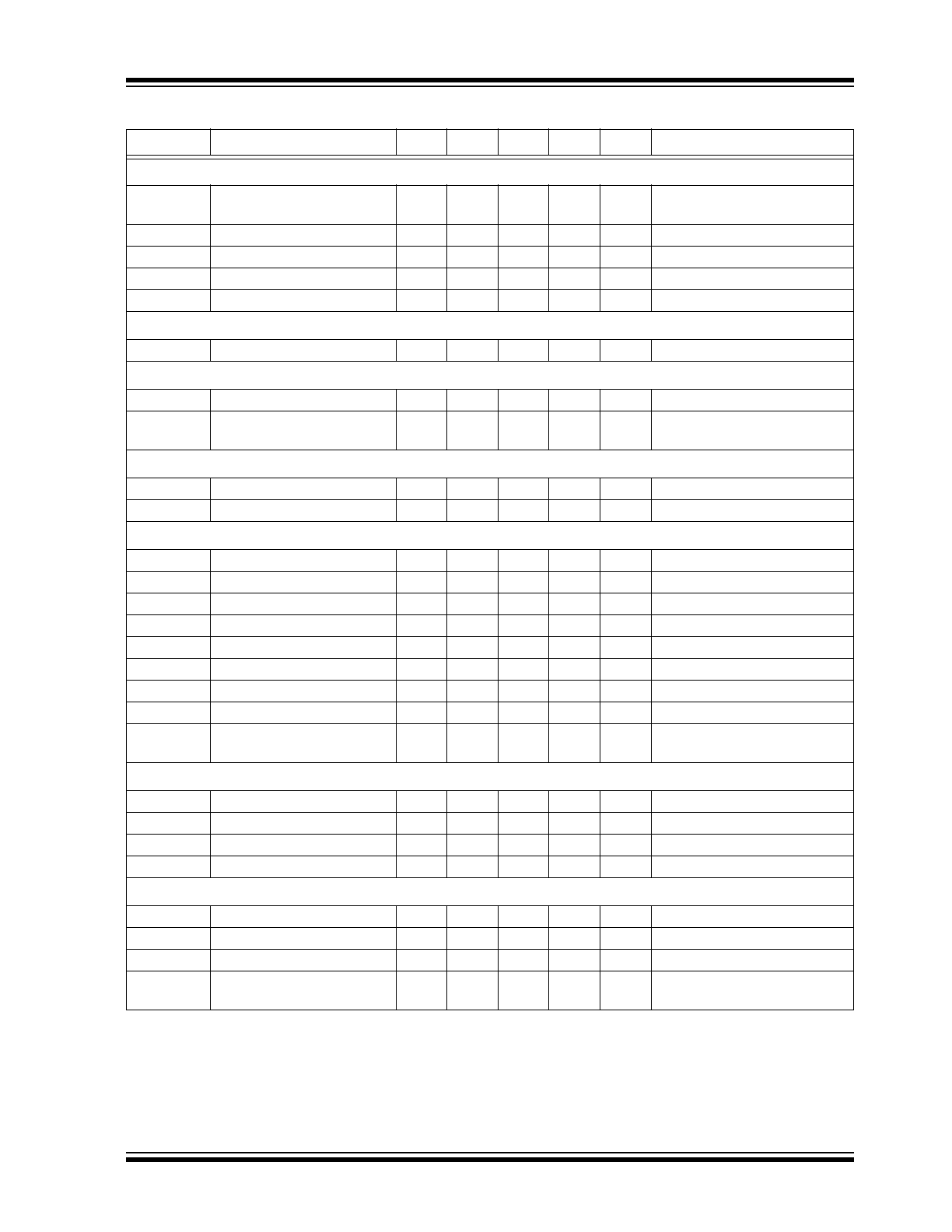
Gate (GATE1, GATE2 and GATE3)
ISOURCE
Gate short circuit current,
sourcing
2
0.2
—
—
A
VGATE = 0V
ISINK
Gate sinking current
2
0.4
—
—
A
VGATE = VDD
TRISE
Gate output rise time
—
—
50
85
ns
CGATE = 1.0nF
TFALL
Gate output fall time
—
—
25
45
ns
CGATE = 1.0nF
DMAX
Maximum duty cycle
2
—
91
—
%
—
Over-voltage Protection (OVP1, OVP2 and OVP3)
VOVP,rising Over-voltage rising trip point
1
4.7
—
5.4
V
OVP rising
Current Sense (CS1, CS2 and CS3)
TBLANK
Leading edge blanking
1
210
—
460
ns
—
TDELAY
Delay to GATE
—
—
—
250
ns
50mV overdrive to the current
sense comparator
Slope Compensation (SC)
CSC(EFF) Effective capacitance
2
0.9
1.0
1.1
nF
—
∆VSC
VDD-to-SC voltage drop
1
1.25
—
3.25
V
RSC = 120kΩ
Internal Transconductance Opamp (Gm1, Gm2 and Gm3)
GB
Gain bandwidth product
2
—
1.0
—
MHz
75pF capacitance at COMP pin
AV
Open loop DC gain
—
65
—
—
dB
Output open
KCOMP
COMP-to-CS divider ratio
2
—
1/12
—
—
—
VCM
Input common-mode range
2
-0.3
—
3.0
V
—
VO
Output voltage range
2
0.7
—
6.75
V
—
Gm
Transconductance
—
500
—
700
μA/V
—
VOFFSET Input offset voltage
—
-5.0
—
5.0
mV
—
IBIAS
Input bias current
2
—
0.5
1.0
nA
—
TR
Recovery delay
2
—
120
—
ns
FDBK = 0V, REF = 0.5V,
PWMD rising
Oscillator (CLOCK)
fOSC1
Oscillator frequency
—
—
500
—
kHz
FCLOCK = 6.0MHz
KSW
Oscillator divider ratio
2
—
12
—
-
—
Phi1
GATE1-GATE2 phase delay
2
—
120
—
°
—
Phi1
GATE1-GATE3 phase delay
2
—
240
—
°
—
Oscillator (CLOCK)
TOFF
CLOCK low time
2
50
—
—
ns
—
TON
CLOCK high time
2
50
—
—
ns
—
VCLOCK,HI CLOCK input high
1
2.0
—
—
V
—
VCLOCK,L
O
CLOCK input low
1
—
—
0.8
V
—
TABLE 1-1:
ELECTRICAL CHARACTERISTICS (CONTINUED) (SHEET 2 OF 3)
1
Symbol
Parameter
Note
Min
Typ
Max
Units Conditions
Note 1:
Applies over the full operating ambient temperature range of 0°C < T
A
< +85°C.
2:
For design guidance only.
HV9989
DS20005296B-page 6
2014 Microchip Technology Inc.
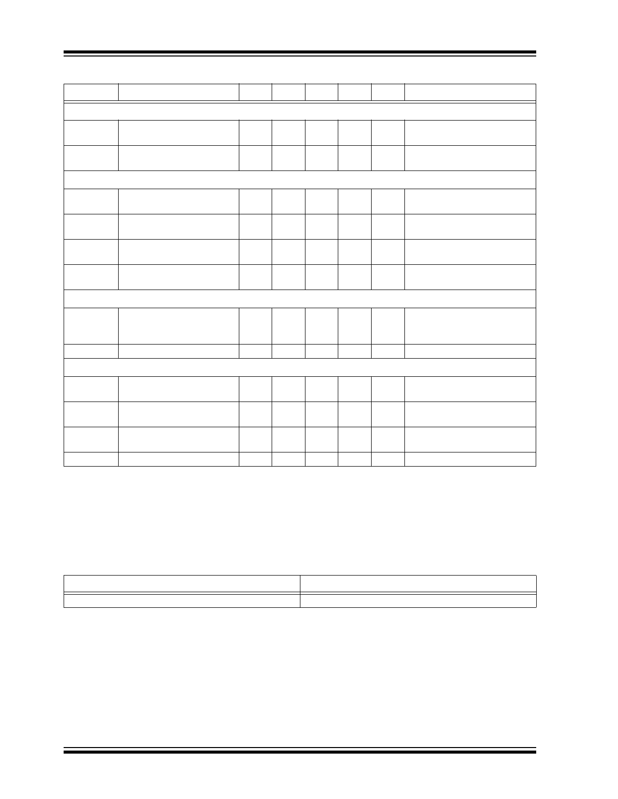
Disconnect Driver (FLT1, FLT2 and FLT3)
TRISE,FAU
LT
Fault output rise time
—
—
—
300
ns
330 pF capacitor at FLTx pin
TFALL,FAU
LT
Fault output fall time
—
—
—
200
ns
330 pF capacitor at FLTx pin
Short Circuit Protection (all three channels)
TBLANK,S
C
Blanking time
1
400
—
800
ns
—
GSC
Gain for short circuit
comparator
—
1.9
2.0
2.1
—
—
Vomin
Minimum current limit
threshold
2
0.15
—
—
V
REF = GND
TOFF
Propagation time for short
circuit detection
—
—
—
250
ns
FDBK = 2 • REF + 0.1V
HICCUP timer
IHC,SOUR
CE
Current source at SKIP pin
used for hiccup mode pro-
tection
—
—
10
—
μA
—
∆VCAP
SKIP voltage swing
2
—
4.0
—
V
—
Low output detection (OVP1, OVP2, OVP3, VIN_SNS, FLG)
VOVP_OS_
F
OVP offset voltage
1
-25
—
25
mV
OVP falling
VOVP_OS_
R
OVP offset voltage
—
40
—
70
mV
OVP rising
VFLG(LOW
)
FLG low voltage
—
0
—
0.4
V
I(FLG) = 1.0mA
VIN_CM
Input common-mode range
2
-0.3
—
5.0
V
—
1
TABLE 1-1:
ELECTRICAL CHARACTERISTICS (CONTINUED) (SHEET 3 OF 3)
1
Symbol
Parameter
Note
Min
Typ
Max
Units Conditions
Note 1:
Applies over the full operating ambient temperature range of 0°C < T
A
< +85°C.
2:
For design guidance only.
TABLE 1-2:
THERMAL RESISTANCE
Package
θja
40-Lead QFN
24°C/W

2014 Microchip Technology Inc.
DS20005296B-page 7
HV9989
2.0
PIN DESCRIPTION
The descriptions of the pins are listed in
Table 2-1
.
TABLE 2-1:
PIN DESCRIPTION (SHEET 1 OF 2)
Pin #
Name
Description
1
VDD1
Power supply pin for channel 1. It can either be connected to the VDD pin or supplied
with an external power supply. It must be bypassed with a low ESR capacitor to their
respective GND1 (at least 0.1 μF). All VDD pins (VDD, VDD1-3) must be connected
together externally.
2
FLT1
Drives external disconnect switches. The disconnect switches are used to protect the
LEDs in case of fault conditions, and also help to provide excellent PWM dimming
response by disconnecting and reconnecting the LEDs from the output capacitor during
PWM dimming.
3
CS1
Senses the source current of the external power FET used with channel 1. It includes a
built-in 210 ns (min) blanking timer.
4
COMP1
Stable closed loop control can be accomplished by connecting a compensation network
between the COMP pin and its GND.
5
FDBK1
Provides output current feedback for channel 1 by using a current sense resistor.
6
REF1
The voltage at this pin sets the output current level for channel 1. Recommended voltage
range for this pin is 0V-1.25V.
7
OVP1
Provides the over voltage protection for the converter. When the voltage at this pin
exceeds 5V, channel 1 of the HV9989 is turned off. The fault is reset by re-enabling the
IC using the EN pin.
8
VIN
Input of the internal 40V linear regulator.
9
VDD
Output of the linear regulator. It maintains a regulated 7.75V as long as the voltage of the VIN
pin is between 10 and 40V. It must be bypassed with a low ESR capacitor to GND (at least 0.1
μF). This pin can be used as a power supply for the three channels.
10
EN
When the pin is pulled below 0.8V, the IC goes into a standby mode and draws minimal current.
11
GND
Ground connection for the common circuitry in the HV9989.
12
COMP2
Stable closed loop control can be accomplished by connecting a compensation network
between the COMP pin and its GND.
13
REF2
The voltage at this pin sets the output current level for channel 2. Recommended voltage
range for this pin is 0-1.25V.
14
OVP2
Provides the over voltage protection for the converter. When the voltage at this pin
exceeds 5V, channel 2 of the HV9989 is turned off. The fault is reset by re-enabling the
IC using the EN pin.
15
SKIP
Programs the hiccup timer for short circuit fault on any of the three channels. A capacitor
to GND programs the hiccup time.
16
SC
Sets the current to program slope compensation voltage ramp at the three CS inputs.
Connect a resistor to GND.
17
PWMD1
Used to PWM dim channel 1.
18
PWMD2
Used to PWM dim channel 2.
19
PWMD3
Used to PWM dim channel 3.
20
NC
No connection.
21
VIN_SNS
When voltage at this pin exceeds any of the voltages at OVP 1-3, the high-impedance
state is issued at the FLG output.
22
FLG
Open-drain logic output reporting a high-impedance state in the case of any of the OVP
1-3 voltages falling below the VIN_SNS voltage. A hysteresis is added at VIN_SNS to
avoid oscillation.
23
CLK
Clock input for the HV9989. The input to the CLK pin should be a TTL compatible square
wave signal. The three channels will switch at 1/12th the switching frequency of the sig-
nal applied at the CLK pin.

HV9989
DS20005296B-page 8
2014 Microchip Technology Inc.
24
OVP3
Provides the over voltage protection for the converter. When the voltage at this pin
exceeds 5V, channel 3 of the HV9989 is turned off. The fault is reset by re-enabling the
IC using the EN pin.
25
REF3
The voltage at this pin sets the output current level for channel 3. Recommended voltage
range for this pin is 0V-1.25V.
26
FDBK3
Provides output current feedback for channel 3 by using a current sense resistor.
27
COMP3
Stable closed loop control can be accomplished by connecting a compensation network
between the COMP pin and its GND.
28
CS3
Used to sense the source current of the external power FET used with channel 3. It
includes a built-in 210 ns (min) blanking timer.
29
FLT3
Used to drive external disconnect switches. The disconnect switches are used to protect
the LEDs in case of fault conditions and also help to provide excellent PWM dimming
response by disconnecting and reconnecting the LEDs from the output capacitor during
PWM dimming.
30
VDD3
Power supply pin for channel 3. It can either be connected to the VDD pin or supplied
with an external power supply. It must be bypassed with a low ESR capacitor to their
respective GND3 (at least 0.1 μF). All VDD pins (VDD, VDD1-3) must be connected
together externally.
31
GATE3
Output gate driver for the external N-channel power MOSFET.
32
GND3
Ground return for channel 3. It is recommended that all the GNDs of the IC be connected
together in a STAR connection at the input GND terminal to ensure best performance.
33
VDD2
Power supply pin for channel 2. It can either be connected to the VDD pin or supplied
with an external power supply. It must be bypassed with a low ESR capacitor to their
respective GND2 (at least 0.1 μF). All VDD pins (VDD, VDD1-3) must be connected
together externally.
34
GND2
Ground return for channel 2. It is recommended that all the GNDs of the IC be connected
together in a STAR connection at the input GND terminal to ensure best performance.
35
GATE2
Output gate driver for the external N-channel power MOSFET.
36
FLT2
Used to drive external disconnect switches. The disconnect switches are used to protect
the LEDs in case of fault conditions and also help to provide excellent PWM dimming
response by disconnecting and reconnecting the LEDs from the output capacitor during
PWM dimming.
37
CS2
Used to sense the source current of the external power FET used with channel 2. It
includes a built-in 210 ns (min) blanking timer.
38
FDBK2
Provides output current feedback for channel 2 by using a current sense resistor.
39
GND1
Ground return for channel 1. It is recommended that all the GNDs of the IC be connected
together in a STAR connection at the input GND terminal to ensure best performance.
40
GATE1
Output gate driver for the external N-channel power MOSFET.
TABLE 2-1:
PIN DESCRIPTION (CONTINUED) (SHEET 2 OF 2)
Pin #
Name
Description

2014 Microchip Technology Inc.
DS20005296B-page 9
HV9989
3.0
FUNCTIONAL DESCRIPTION
3.1
Power Topology
HV9989 is a three-channel, switch-mode converter,
LED driver designed to control a continuous conduction
mode boost or SEPIC device in a constant frequency
mode. The IC includes an internal linear regulator,
which operates from 10 to 40V input voltages. This
device can also be powered directly using the VDD
pins and bypassing the internal linear regulator.
HV9989 includes features typically required in LED
drivers such as open LED protection, output short cir-
cuit protection, linear and PWM dimming, programma-
ble input current limiting and accurate control of the
LED current. A high current gate drive output enables
the controller to be used in high power converters.
HV9989 is ideally suited for back-light applications
using either RGB or multi-channel white LED
configurations.
3.2
Power Supply to the IC (VIN, VDD,
VDD1-3)
The HV9989 can be powered directly from its VIN pin
that takes a voltage up to 40V. When a voltage is
applied at the VIN pin, the HV9989 tries to maintain a
constant 7.75V (typ) at the VDD pin. The regulator also
has a built in under-voltage lockout which shuts off the
IC if the voltage at the VDD pin falls below the UVLO
threshold. By connecting this VDD pin to the individual
VDD pins of the three channels, the internal regulator
can be used to power all three channels in the IC.
In case the internal regulator is not utilized, an external
power supply (7-9V) can be used to power the IC. In
this case, the power supply is directly connected to the
VDD pins and the VIN pin is left unconnected.
All four VDD pins must be bypassed by a low ESR
capacitor (≥0.1 µF) to provide a low impedance path for
the high frequency current of the output gate driver.
These capacitors must be referenced to the individual
grounds for proper noise rejection. Also, in all cases,
the four VDD pins must be connected together
externally.
The input current drawn from the external power supply
(or VIN pin) is a sum of the 4 mA current drawn by the
all the internal circuitry (for all three channels) and the
current drawn by the gate drivers (which in turn
depends on the switching frequency and the gate
charge of the external FET).
In the preceding equation, f
S
is the switching frequency
of the converters and Q
G1-3
are the gate charges of the
external FETs (which can be obtained from the FET
data sheets).
The EN pin is a TTL-compatible input used to disable
the IC. Pulling the EN pin to GND will shut down the IC
and reduce the quiescent current drawn by the IC to be
lower than 500 μA. If the enable function is not
required, the EN pin can be connected to VDD.
3.3
Clock Input (CLK)
The switching frequency of the converters are set by
using a TTL-compatible square wave input at the CLK
pin. The switching frequencies of the three converters
will be 1/12th the frequency of the external clock.
3.4
Current Sense (CS1-3)
The current sense input is used to sense the source
current of the switching FET. The CS input of the
HV9989 includes a built-in 100 ns (minimum) blanking
time to prevent spurious turn off due to the initial current
spike when the FET turns on.
The IC includes an internal resistor divider network,
which steps down the voltage at the COMP pins by a
factor of 12 (including the internal diode drop). This
stepped-down voltage is given to one of the
comparators as the current reference.
It is recommended that the sense resistor R
CS
be cho-
sen so as to provide about 250 mV current sense signal.
3.5
Slope Compensation
For continuous conduction mode converters operating in
the Constant Frequency mode, slope compensation
becomes necessary to ensure stability of the peak cur-
rent mode controller, if the operating duty cycle is greater
than 0.5. Choosing a slope compensation which is one
half of the down slope of the inductor current ensures
that the converter will be stable for all duty cycles.
Slope compensation in the HV9989 can be pro-
grammed by a single resistor at SC input common for
all three channels. Assuming a down slope of DS (A/
ms) for the inductor current, the SC resistor can be
computed as:
where R
CS
is the current sense resistor at the CS
X
inputs.
I
IN
4mA
Q
G1
Q
G2
Q
G3
+
+
+
f
s
=
R
SC
2
V
DD
V
SC
–
DS 10
6
R
CS
C
SC EFF
--------------------------------------------------------------
11
V
DS R
CS
C
SC EFF
-----------------------------------------------
=
HV9989
DS20005296B-page 10
2014 Microchip Technology Inc.
3.6
Control of the LED Current
The LED currents in the HV9989 are controlled in a
closed-loop manner. The current references which set
the three LED currents are provided at the REF pins
(REF1-3). This reference voltage is compared to the
FDBK voltages (FDBK1-3) which sense the LED cur-
rents in the three channels using current sense resis-
tors. The HV9989 includes three 1MHz
transconductance amplifiers with tri-state outputs,
which are used to close the feedback loops and provide
accurate current control. The compensation networks
are connected at the COMP pins (COMP1-3).
The outputs of the op amps are buffered and connected
to the current sense comparators using 12:1 dividers.
The buffer helps to prevent the integrator capacitor from
discharging during the PWM dimming state.
The outputs of the op amps are controlled by the signal
applied to the PWMD pins (PWMD1-3). When PWMD
is high, the output of the op amp is connected to the
COMP pin. When PWMD is low, the output is left open.
This enables the integrating capacitor to hold the
charge when the PWMD signal has turned off the gate
drive. When the IC is enabled, the voltage on the inte-
grating capacitor will force the converter into steady
state almost instantaneously.
3.7
Linear Dimming
Linear dimming can be accomplished in the HV9989 by
varying the voltages at the REF pins. Note that since
the HV9989 is a peak current mode controller, it has a
minimum on-time for the GATE outputs. This minimum
on-time will prevent the converters from completely
turning off even when the REF pins are pulled to GND.
Thus, linear dimming cannot accomplish true zero LED
current. To get zero LED current, PWM dimming has to
be used. Note that different signals can be connected
to the three REF pins if desired, and they need not be
connected together.
Due to the offset voltage of the short circuit comparator,
as well as the non-linearity of the X2 gain stage, pulling
the REF pin very close to GND would cause the inter-
nal short circuit comparator to trigger and shut down
the IC. To overcome this, the output of the gain stage is
limited to 125mV (minimum), allowing the REF pin to
be pulled all the way to 0V without triggering the short
circuit comparator.
3.8
PWM Dimming
PWM dimming in HV9989 can be accomplished using
a TTL-compatible square wave source at the PWMD1-
3 pins.
HV9989 has an enhanced PWM dimming capability,
which allows PWM dimming to widths less than one
switching cycle with no drop in the LED current.
The enhanced PWM dimming performance of the
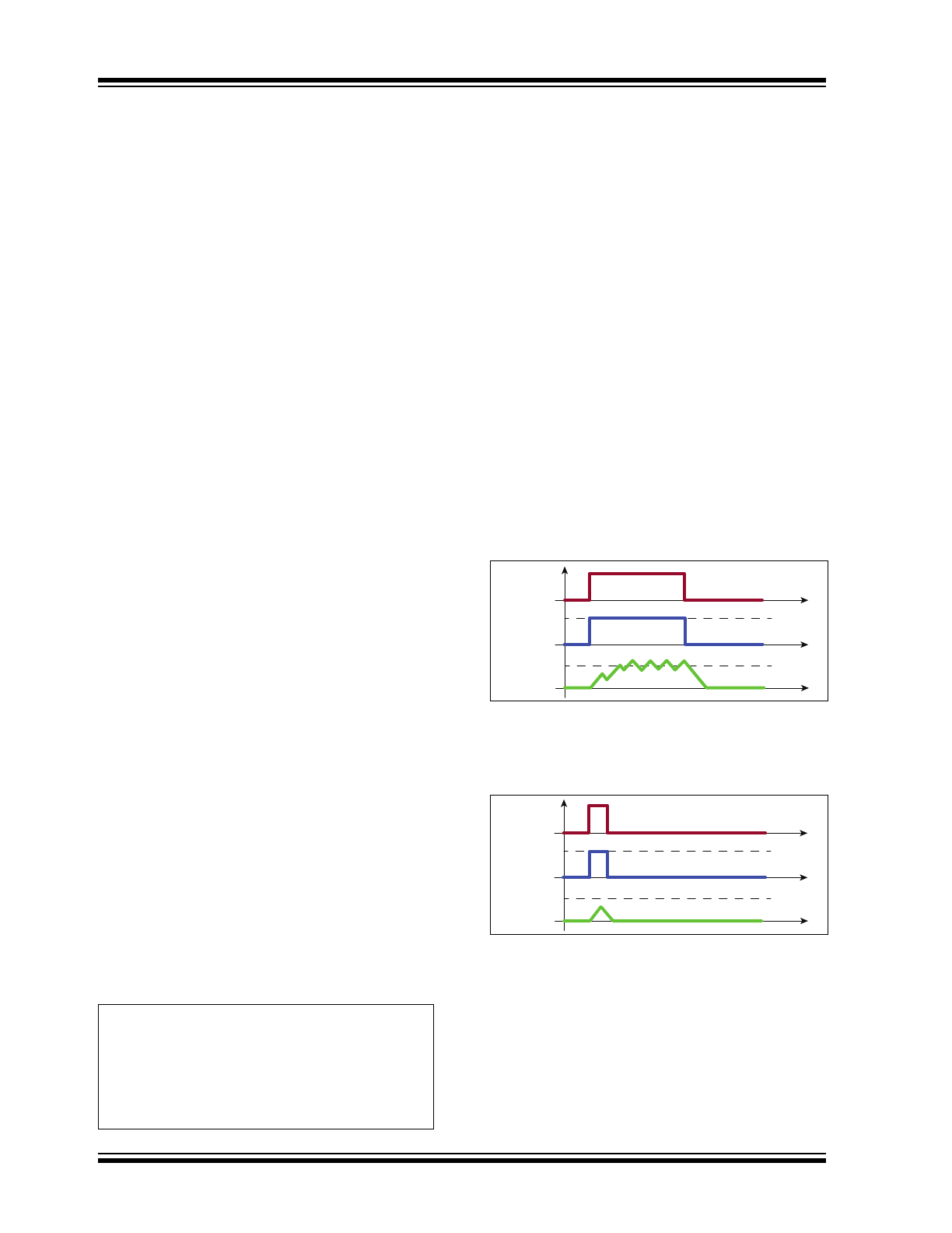
HV9989 can be best explained by considering typical
boost converter circuits without this functionality. When
the PWM dimming pulse becomes very small (less than
one switching cycle for a DCM design or less than a few
switching cycles for a CCM design), the boost con-
verter is turned off before the input current can reach its
steady state value. This causes the input power to
drop, which is manifested in the output as a drop in the
LED current (
Figure 3-1
and
Figure 3-2
for a CCM
design).
FIGURE 3-1:
PWM DIMMING WITH
DIMMING ON-TIME FAR
GREATER THAN ONE
SWITCHING TIME PERIOD
FIGURE 3-2:
PWM DIMMING WITH
DIMMING ON-TIME
EQUAL TO ONE
SWITCHING TIME PERIOD
In the above figures, I
O
(SS) and I
L
(SS) refer to the
steady state values (PWMD = 100%) for the output cur-
rent and inductor current respectively. As can be seen,
the inductor current does not rise enough to trip the CS
comparator. This causes the closed loop amplifier to
lose control of the LED current and COMP rails to VDD.
Note:
This control IC is a peak current mode control-
ler; therefore, pulling the REF pin to zero will
not cause the LED current to go to zero. The
converter will still be operating at its minimum
on-time causing a very small current to flow
through the LEDs. To get zero LED current,
the PWMD input has to be pulled to GND.
PWMD
I
LED
I
INDUCTOR
I
O
(SS)
I
O
(SS)
PWMD
I
LED
I
INDUCTOR
I
O
(SS)
I
L
(SS)