

2014 Microchip Technology Inc.
DS20005295B-page 1
HV9982
Features
• Switch mode controller for single-switch convert-
ers
• Closed loop control of output current
- Buck
- Boost
- SEPIC
• High PWM dimming ratio
• Internal 40V linear regulator
• Constant frequency operation
• Programmable slope compensation
• Linear and PWM dimming
• +0.2A/-0.4A gate drives for the switching FETs
• Output short circuit protection
• Output over voltage protection
• Hiccup-mode protection
• Analog control of PWM dimming
Applications
• RGB backlight applications
• Multiple string, white-LED driver applications
Description
HV9982 is a three-channel, closed loop, peak-current
mode PWM controller designed to drive a constant out-
put current. It can be used for driving either RGB LEDs
or multiple channels of white LEDs.
HV9982 includes a 40V linear regulator which provides
an 8.0V supply to power the IC. The switching frequen-
cies of the three converters are controlled by an exter-
nal clock signal. The channels operate at a switching
frequency of 1/12th of the external clock frequency and
are positioned 120
°
out-of-phase to reduce the input
current ripple. Each converter is driven by a peak cur-
rent mode controller with output current feedback.
The three output currents can be individually dimmed
using either linear or PWM dimming. The IC also
includes three disconnect FET drivers, which enable
high PWM-dimming ratios and also help to disconnect
the input in case of an output short-circuit condition.
HV9982 includes a Hiccup-mode protection for both
open LED and short-circuit condition with automatic
recovery when the fault clears.
Three-Channel, Closed-Loop, Switch Mode
LED Drive IC

HV9982
DS20005295B-page 2
2014 Microchip Technology Inc.
TO OUR VALUED CUSTOMERS
It is our intention to provide our valued customers with the best documentation possible to ensure successful use of your Microchip
products. To this end, we will continue to improve our publications to better suit your needs. Our publications will be refined and
enhanced as new volumes and updates are introduced.
If you have any questions or comments regarding this publication, please contact the Marketing Communications Department via
E-mail at
docerrors@microchip.com
. We welcome your feedback.
Most Current Data Sheet
To obtain the most up-to-date version of this data sheet, please register at our Worldwide Web site at:
http://www.microchip.com
You can determine the version of a data sheet by examining its literature number found on the bottom outside corner of any page.
The last character of the literature number is the version number, (e.g., DS30000000A is version A of document DS30000000).
Errata
An errata sheet, describing minor operational differences from the data sheet and recommended workarounds, may exist for current
devices. As device/documentation issues become known to us, we will publish an errata sheet. The errata will specify the revision
of silicon and revision of document to which it applies.
To determine if an errata sheet exists for a particular device, please check with one of the following:
• Microchip’s Worldwide Web site;
http://www.microchip.com
• Your local Microchip sales office (see last page)
When contacting a sales office, please specify which device, revision of silicon and data sheet (include literature number) you are
using.
Customer Notification System
Register on our web site at
www.microchip.com
to receive the most current information on all of our products.
2014 Microchip Technology Inc.
DS20005295B-page 3
HV9982
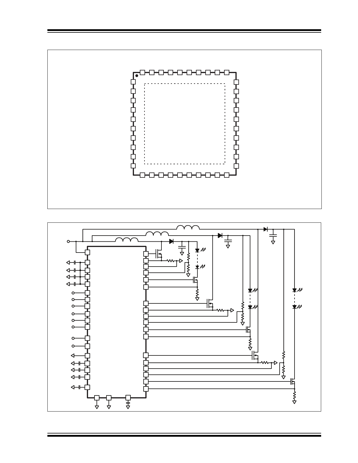
Pin Diagram
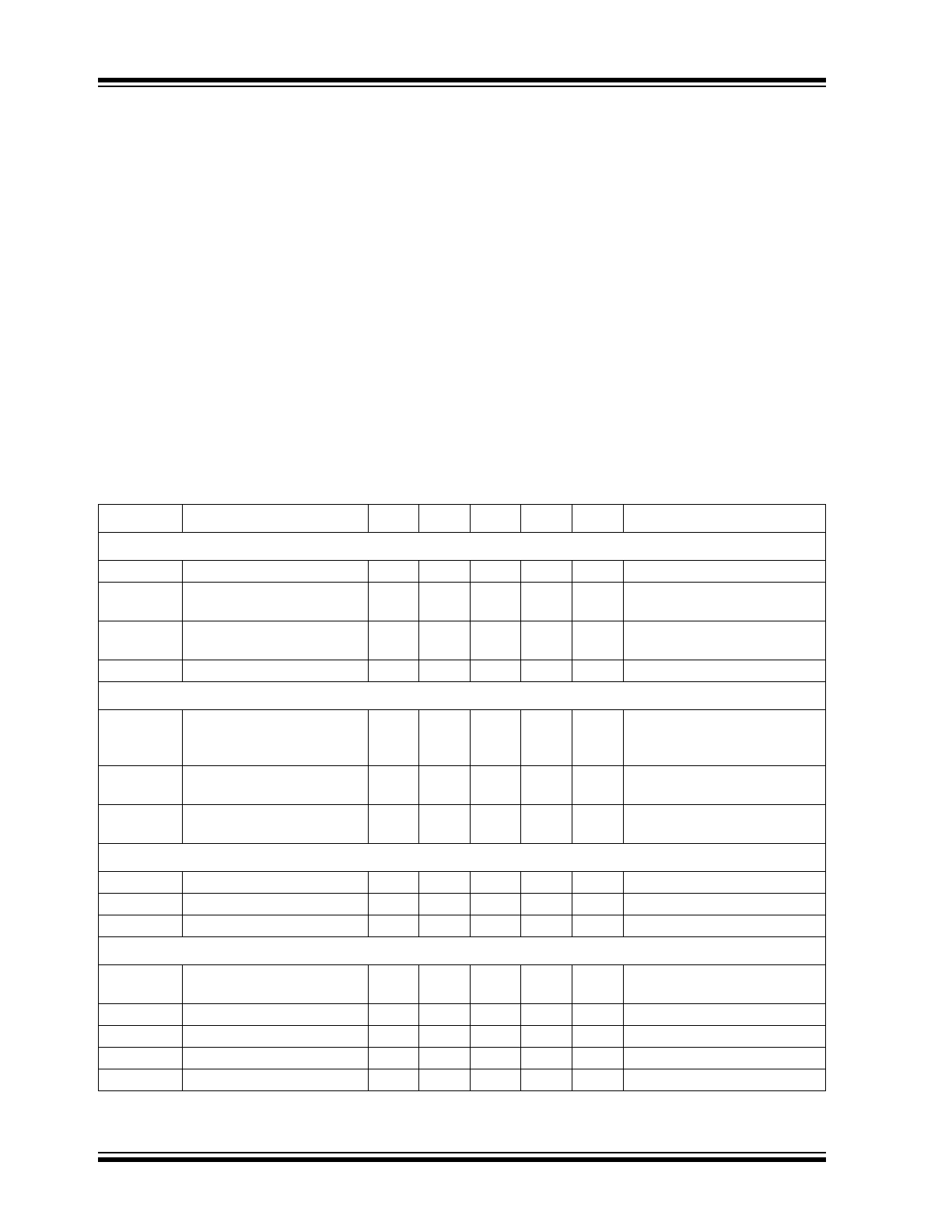
Typical Application Circuit
40-Lead QFN
VDD3
FLT3
CS3
COMP3
FDBK3
REF3
OVP3
CLK
NS
S2
GND
1
10
11
20
40
30
21
31
VDD1
FLT1
CS1
COMP1
FDBK1
REF1
OVP1
VIN
VDD
EN
GND
COMP2
REF2
OVP2
SKIP
RAMP
PWMD1
PWMD2
PWMD3
S1
GATE1
GND1
FDBK2
CS2
FLT2
GATE2
GND2
VDD2
GND3
GATE3
GATE1
CS1
GND1
FLT1
FDBK1
GATE2
CS
GND2
FLT2
FDBK2
GATE3
CS3
OVP3
FLT3
FDBK3
OVP1
OVP2
GND3
VIN
VDD
VDD1
VDD2
VDD3
PWMD1
PWMD2
PWMD3
REF1
REF2
REF3
EN
CLK
GND
COMP1
COMP2
COMP3
SKIP
S2
RAMP
S1
HV9982
HV9982
DS20005295B-page 4
2014 Microchip Technology Inc.
1.0
ELECTRICAL
CHARACTERISTICS
ABSOLUTE MAXIMUM RATINGS
†
V
IN
to GND........................................................ -0.5V to +45V
V
DD
to GND, V
DD
1-3 to GND..........................--0.3V to +10V
All other pins to GND .............................-0.3V to (V
DD
+ 0.3V)
Operating temperature ..................................-40°C to +125°C
Storage temperature .....................................-65°C to +150°C
Continuous power dissipation (T
A
= +25°C).............5000 mW
† Notice: Stresses above those listed under “Absolute Maxi-
mum Ratings” may cause permanent damage to the device.
This is a stress rating only and functional operation of the
device at those or any other conditions, above those indi-
cated in the operational listings of this specification, is not
implied. Exposure to maximum rating conditions for extended
periods may affect device reliability.
1.1
ELECTRICAL SPECIFICATIONS
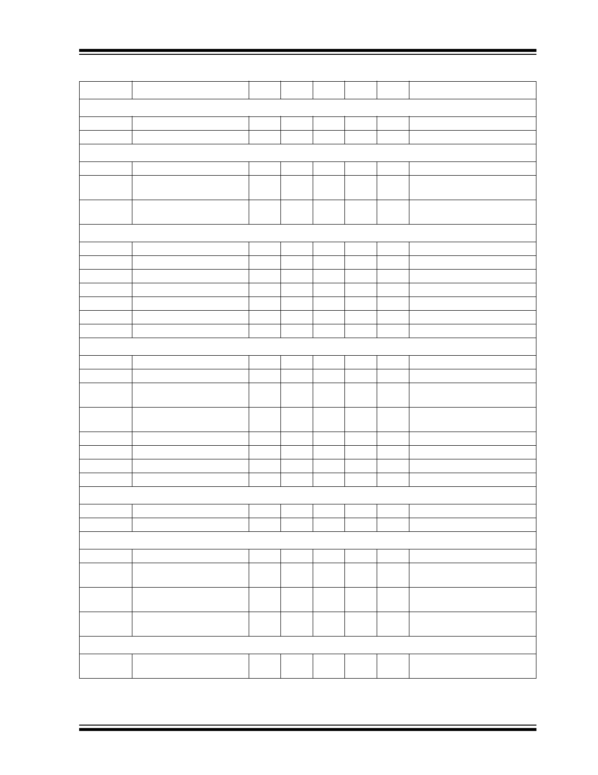
TABLE 1-1:
ELECTRICAL CHARACTERISTICS (SHEET 1 OF 3)
1
Symbol
Parameter
Note
Min
Typ
Max
Units Conditions
Input
V
INDC
Input DC supply voltage
1
10
-
40
V
DC input voltage
I
INSD
Shut-down mode supply
current
1
-
-
500
μA
EN ≤ 0.8V
I
IN
Supply current
-
-
-
4.5
mA
EN ≥ 2.0V; PWMD1 = PWMD2
= PWMD3 = GND
R
EN
Pull-down resistor
-
75
130
160
kΩ
V
EN
= 5.0V
Internal Regulator
V
DD
Internally regulated voltage
1
7.25
7.75
8.25
V
V
IN
= 12-40V; EN = HIGH;
PWMD1-3 = V
DD
; GATE1-3 =
1nF; CLK = 6MHz
UVLO
V
DD
under voltage lockout
threshold
-
6.0
-
6.5
V
V
DD
falling
UVLO
HYST
V
DD
under voltage hystere-
sis
-
-
500
-
mV
V
DD
rising
PWM Dimming (PWMD1, PWMD2 and PWMD3)
V
PWMD(lo)
PWMD input low voltage
1
-
-
0.8
V
---
V
PWMD(hi)
PWMD input high voltage
1
2.0
-
-
V
---
R
PWMD
PWMD pull down resistor
-
75
130
160
kΩ
V
PWMD
= 5.0V
Gate (GATE1, GATE2 and GATE3)
I
SOURCE
Gate short circuit current,
sourcing
2
0.2
-
-
A
V
GATE
= 0V
I
SINK
Gate sinking current
2
0.4
-
-
A
V
GATE
= VDD
T
RISE
Gate output rise time
-
-
-
85
ns
C
GATE
= 1.0nF
T
FALL
Gate output fall time
-
-
-
45
ns
C
GATE
= 1.0nF
D
MAX
Maximum duty cycle
2
-
91.7
-
%
---
Note 1:
Applies over the full operating ambient temperature range of 0°C < T
A
< +85°C.
2:
For design guidance only.
2014 Microchip Technology Inc.
DS20005295B-page 5
HV9982
Over-voltage Protection (OVP1, OVP2 and OVP3)
V
OVP,rising
Over voltage rising trip point
1
4.5
5.0
5.5
V
OVP rising
V
OVP,HYST
Over voltage hysteresis
-
-
0.5
-
V
OVP falling
Current Sense (CS1, CS2 and CS3)
T
BLANK
Leading edge blanking
1
100
-
250
ns
---
T
DELAY
Delay to output of gate
1
-
-
200
ns
100mV overdrive to the current
sense
R
DIS
Discharge resistance for
slope compensation
1
-
-
650
Ω
Gate = Low
Internal Transconductance Opamp (G
m1
, G
m2
and G
m3
)
GB
Gain bandwidth product
2
-
1.0
-
MHz
75pF capacitance at COMP pin
A
V
Open loop DC gain
-
65
-
-
dB
Output open
V
CM
Input common-mode range
2
-0.3
-
3.0
V
---
V
O
Output voltage range
2
0.7
-
V
DD
V
---
G
m
Transconductance
-
500
600
700
μA/V ---
V
OFFSET
Input offset voltage
-
-5.0
-
5.0
mV
---
I
BIAS
Input bias current
2
-
0.5
1.0
nA
---
Oscillator (CLOCK)
f
OSC1
Oscillator frequency
-
-
500
-
kHz
F
CLOCK
= 6.0MHz
K
SW
Oscillator divider ratio
2
-
12
-
-
---
Phi1
GATE1 - GATE2 phase
delay
2
-
120
-
°
---
Phi1
GATE1 - GATE3 phase
delay
2
-
240
-
°
---
T
OFF
CLOCK low time
2
50
-
-
ns
---
T
ON
CLOCK high time
2
50
-
-
ns
---
V
CLOCK,HI
CLOCK input high
1
2.0
-
-
V
---
V
CLOCK,LO
CLOCK input low
1
-
-
0.8
V
---
Disconnect Driver (FLT1, FLT2 and FLT3)
T
RISE,FAULT
Fault output rise time
-
-
-
450
ns
330pF capacitor at FAULT pin
T
FALL,FAULT
Fault output fall time
-
-
-
200
ns
330pF capacitor at FAULT pin
Short Circuit Protection (all three channels)
T
BLANK,SC
Blanking time
1
400
-
700
ns
---
G
SC
Gain for short circuit com-
parator
-
1.85
2.00
2.15
-
---
V
omin
Minimum current limit
threshold
2
0.15
-
0.25
V
REF = GND
T
OFF
Propagation time for short
circuit detection
-
-
-
250
ns
FDBK = 2 • REF + 0.1V
HICCUP timer
I
HC,SOURCE
Current source at SKIP pin used
for hiccup mode protection
-
-
10
-
μA
---
TABLE 1-1:
ELECTRICAL CHARACTERISTICS (CONTINUED) (SHEET 2 OF 3)
1
Symbol
Parameter
Note
Min
Typ
Max
Units Conditions
Note 1:
Applies over the full operating ambient temperature range of 0°C < T
A
< +85°C.
2:
For design guidance only.
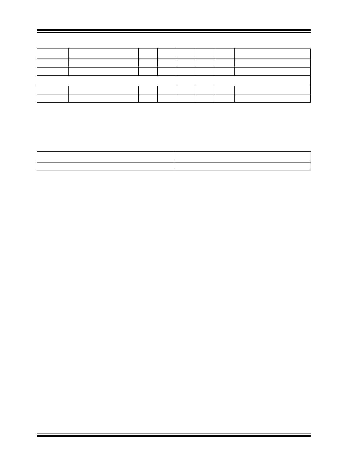
HV9982
DS20005295B-page 6
2014 Microchip Technology Inc.
V
TH(H)
High threshold at SKIP pin
2
-
5.0
-
V
---
V
TH(L)
Low threshold at SKIP pin
2
-
0.1
-
V
---
C
RAMP
for Analog Control of PWM Dimming
F
RAMP,min
Minimum frequency
-
-
110
-
Hz
C
RAMP
= 10nF
F
RAMP,max
Maximum frequency
-
-
1250
-
Hz
C
RAMP
= 1.0nF
1
TABLE 1-1:
ELECTRICAL CHARACTERISTICS (CONTINUED) (SHEET 3 OF 3)
1
Symbol
Parameter
Note
Min
Typ
Max
Units Conditions
Note 1:
Applies over the full operating ambient temperature range of 0°C < T
A
< +85°C.
2:
For design guidance only.
TABLE 1-2:
THERMAL RESISTANCE
Package
θja
40-Lead QFN
24°C/W

2014 Microchip Technology Inc.
DS20005295B-page 7
HV9982
2.0
PIN DESCRIPTION
The descriptions of the pins are listed in
Table 2-1
.
TABLE 2-1:
PIN DESCRIPTION (SHEET 1 OF 2)
Pin #
Name
Description
1
VDD1
Power supply pin for channel 1. It can either be connected to the VDD pin or supplied
with an external power supply. It must be bypassed with a low ESR capacitor to GND1
(at least 0.1 μF). All VDD pins (VDD, VDD1-3) must be connected together externally.
An external supply (7.0-9.0V) can be connected to these pins to power the IC if the
internal regulator is not used.
2
FLT1
Used to drive an external disconnect switch. The disconnect switch is used to protect the
LEDs in case of fault conditions and also help to provide excellent PWM dimming
response by disconnecting and reconnecting the LEDs from the output capacitor during
PWM dimming.
3
CS1
Used to sense the source current of the external power FET used with channel 1. It
includes a built-in 100 ns (min) blanking timer. An R-C network at this pin programs the
slope compensation. Refer to the Slope Compensation section for additional informa-
tion.
4
COMP1
Stable closed loop control for channel 1 can be accomplished by connecting a
compensation network between each COMP1 pin and GND1.
5
FDBK1
Output current feedback input for channel 1. It receives a voltage signal from an external
sense resistor.
6
REF1
The voltage at this pin sets the output current level for channel 1. Recommended voltage
range for this pin is 0-1.25V.
7
OVP1
Provides the over-voltage protection for the channel 1. When the voltage at this pin
exceeds 5.0V, the HV9982 is turned off and the fault timer starts. Upon completion of the
fault timer the IC attempts to restart.
8
VIN
Input of the internal 40V linear regulator.
9
VDD
Output of the linear regulator. It maintains a regulated 7.75V as long as the voltage of the
VIN pin is between 10 and 40V. It must be bypassed with a low ESR capacitor to GND
(at least 0.1 μF). Can be used as a power supply for the three channels.
10
EN
When pin is pulled below 0.8V, the IC goes into a standby mode and draws minimal
current.
11
GND
Ground connection for the common circuitry in the HV9982.
12
COMP2
Stable closed loop control for channel 2 can be accomplished by connecting a
compensation network between each COMP2 pin and GND2.
13
REF2
The voltage at this pin sets the output current level for channel 2. Recommended voltage
range for this pin is 0-1.25V.
14
OVP2
Provides the over voltage protection for the channel 2. When the voltage at this pin
exceeds 5.0V, the HV9982 is turned off and the fault timer starts. Upon completion of the
fault timer the IC attempts to restart.
15
SKIP
Programs the hiccup timer for fault conditions. A capacitor to GND programs the hiccup
time.
16
RAMP
Provides a ramp signal which is used while dimming the channels with pulse-width mod-
ulation with an analog input. A capacitor to GND programs the PWM-dimming frequency.
17
PWMD1
PWM dimming of the three channels is accomplished by using the PWMD pins. If S1 is
LOW, then the three pins directly control the PWM dimming of the three channels and a
square wave input should be applied at these pins. If S1 is high, then a 0-2.0V analog
signal should be applied at these pins. The PWM dimming is then done by comparing
the analog voltage to the voltage at the RAMP pin.
18
PWMD2
19
PWMD3
20
S1
Digital input pins which select the operating mode of the PWMD inputs. Refer to the
PWM dimming section for additional information.
21
S2
22
NC
No connect.

HV9982
DS20005295B-page 8
2014 Microchip Technology Inc.
23
CLK
Clock input for the HV9982. The input to the CLK pin should be a TTL compatible square
wave signal. The three channels will switch at 1/12th the switching frequency of the
signal applied at the CLK pin.
24
OVP3
Provides the over voltage protection for the channel 3. When the voltage at this pin
exceeds 5.0V, the HV9982 is turned off and the fault timer starts. Upon completion of the
fault timer the IC attempts to restart.
25
REF3
The voltage at this pin sets the output current level for channel 3. Recommended voltage
range for this pin is 0-1.25V.
26
FDBK3
Output current feedback input for channel 3. It receives a voltage signal from an external
sense resistor.
27
COMP3
Stable closed loop control for channel 3 can be accomplished by connecting a
compensation network between each COMP3 pin and GND3.
28
CS3
Used to sense the source current of the external power FET used with channel 3. It
includes a built-in 100 ns (min) blanking timer. An R-C network at this pin programs the
slope compensation. Refer to the Slope Compensation section for additional informa-
tion.
29
FLT3
Used to drive an external disconnect switch. The disconnect switch is used to protect the
LEDs in case of fault conditions and also help to provide excellent PWM-dimming
response by disconnecting and reconnecting the LEDs from the output capacitor during
PWM dimming.
30
VDD3
Power supply pin for channel 3. It can either be connected to the VDD pin or supplied
with an external power supply. It must be bypassed with a low ESR capacitor to GND3
(at least 0.1 μF). All VDD pins (VDD, VDD1-3) must be connected together externally.
An external supply (7.0-9.0V) can be connected to these pins to power the IC if the inter-
nal regulator is not used.
31
GATE3
Output gate drive for an external N-channel power MOSFET.
32
GND3
Ground return for channel 3. It is recommended that all the GNDs of the IC be connected
together in a STAR connection at the input GND terminal to ensure best performance.
33
VDD2
Power supply pin for channel 2. It can either be connected to the VDD pin or supplied
with an external power supply. It must be bypassed with a low ESR capacitor to GND2
(at least 0.1 μF). All VDD pins (VDD, VDD1-3) must be connected together externally.
An external supply (7.0-9.0V) can be connected to these pins to power the IC if the inter-
nal regulator is not used.
34
GND2
Ground return for channel 2. It is recommended that all the GNDs of the IC be connected
together in a STAR connection at the input GND terminal to ensure best performance.
35
GATE2
Output gate drive for an external N-channel power MOSFET.
36
FLT2
Used to drive an external disconnect switch. The disconnect switch is used to protect the
LEDs in case of fault conditions and also help to provide excellent PWM-dimming
response by disconnecting and reconnecting the LEDs from the output capacitor during
PWM dimming.
37
CS2
Used to sense the source current of the external power FET used with channel 2. It
includes a built-in 100 ns (min) blanking timer. An R-C network at this pin programs the
slope compensation. Refer to the Slope Compensation section for additional informa-
tion.
38
FDBK2
Output current feedback input for channel 2. It receives a voltage signal from an external
sense resistor.
39
GND1
Ground return for channel 1. It is recommended that all the GNDs of the IC be connected
together in a STAR connection at the input GND terminal to ensure best performance.
40
GATE1
Output gate drive for an external N-channel power MOSFET.
TABLE 2-1:
PIN DESCRIPTION (CONTINUED) (SHEET 2 OF 2)
Pin #
Name
Description

2014 Microchip Technology Inc.
DS20005295B-page 9
HV9982
3.0
FUNCTIONAL DESCRIPTION
3.1
Power Topology
HV9982 is a three-channel, switch-mode converter
LED driver designed to control a continuous conduction
mode buck, boost or SEPIC converter in a constant fre-
quency mode. The IC includes an internal linear regu-
lator, which operates from input voltages 10V to 40V.
The IC can also be powered directly using the VDD
pins and bypassing the internal linear regulator. The IC
includes features typically required in LED drivers such
as open LED protection, output short circuit protection,
linear and PWM dimming, programmable input current
limiting, and accurate control of the LED current. A high
current gate drive output enables the controller to be
used in high power converters. The IC is ideally suited
for backlight application using either RGB or multi-
channel white LED configurations.
3.2
Power Supply to the IC (VIN, VDD,
VDD1-3)
HV9982 can be powered directly from its VIN pin which
withstands a voltage up to 40V. When a voltage is
applied at the VIN pin, the HV9982 tries to maintain a
constant 7.75V (typ) at the VDD pin. The regulator also
has a built in under-voltage lockout, which shuts off the
IC if the voltage at the VDD pin falls below the UVLO
threshold. By connecting this VDD pin to pins VDD1-3
of the other three channels, the internal regulator can
be used to power all three channels in the IC.
If the internal regulator is not utilized, an external power
supply (7.0-9.0V) can be used to power the IC. In this
case, the power supply is directly connected to the
VDD1-3 pins and the VIN pin is left unconnected.
All four VDD pins must by bypassed by a low ESR
capacitor (≥0.1 µF) to provide a low impedance path for
the high frequency current of the output gate driver.
These capacitors must be referenced to the individual
grounds for proper noise rejection (see
3.13 “Layout
Considerations”
). Also, in all cases, the four VDD pins
must be connected together externally.
The input current drawn from the external power supply
(or VIN pin) is a sum of the 4.5 mA (max) current drawn
by all the internal circuitry and the current drawn by the
gate drivers (which in turn depends on the switching
frequency and the gate charge of the external FET).
In the above equation, f
S
is the switching frequency of
the converters and Q
g1-3
are the gate charges of the
external FETs (which can be obtained from the FET
data sheets).
The EN pin is a TTL-compatible input used to disable
the IC. Pulling the EN pin to GND will shut down the IC
and reduce the quiescent current drawn by the IC to be
less than 500 μA. If the enable function is not required,
the EN pin can be connected to VDD.
3.3
Clock Input (CLK)
The switching frequency of the converters is set by
using a TTL-compatible square wave input at the CLK
pin. The switching frequencies of the three converters
will be 1/12
TH
the frequency of the external clock.
3.4
Current Sense (CS1-3)
The current sense input is used to sense the source
current of the switching FET. Each CS input of the
HV9982 includes a built-in, 100 ns (minimum) blanking
time to prevent spurious turn off due to the initial current
spike when the FET turns on.
The IC includes an internal, resistor-divider network,
which steps down the voltage at the COMP pins by a
factor of 13. This voltage is used as the reference for
the current sense comparators. Since the maximum
voltage of the COMP pin is (V
DD
– 1.0V), this voltage
determines the maximum reference current for the cur-
rent sense comparator, and thus the maximum inductor
current.
The current sense resistor, R
CS
, should be chosen so
that the input inductor current is kept below the satura-
tion current level of the input inductor. For discontinu-
ous conduction mode of operation, no slope
compensation is necessary. In this case, the current
sense resistor is chosen as:
where I
IN,pk
is the maximum desired peak input current.
For continuous conduction mode converters operating
in the constant frequency mode, slope compensation
becomes necessary to ensure stability of the peak cur-
rent mode controller, if the operating duty cycle is
greater than 0.5. This factor must also be accounted for
when determining R
CS
(see
3.5 “Slope Compensa-
tion”
).
3.5
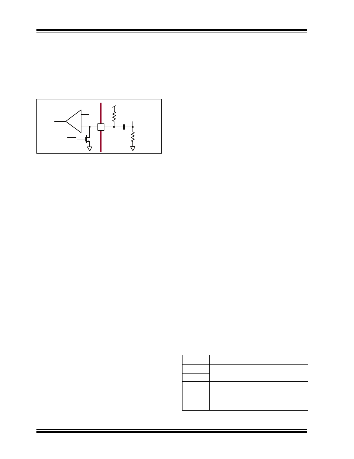
Slope Compensation
Choosing a slope compensation, which is one half of
the down slope of the inductor current, ensures that the
converter will be stable for all duty cycles.
Slope compensation in the HV9982 can be pro-
grammed by two external components, see
Figure 3-1
.
A resistor for V
DD
sets a current, which is almost con-
stant since the V
DD
voltage is much larger than the volt-
age at the CS pin. This current flows into the capacitor
and produces a ramp voltage across the capacitor. The
voltage at the CS pin is then the sum of the voltage
I
IN
4.5mA
Q
g1
Q
g2
Q
g3
+
+
+
f
s
=
R
CS
V
DD
1.0V
–
13 I
IN pk
-----------------------------
=
HV9982
DS20005295B-page 10
2014 Microchip Technology Inc.
across the capacitor and the voltage across the current
sense resistor. The voltage across the capacitor pro-
vides the required slope compensation. When the
GATE turns off, an internal pull down FET discharges
the capacitor. The 650Ω resistance of the internal FET
will prevent the voltage at the CS pin from going all the
way to zero.
FIGURE 3-1:
SLOPE COMPENSATION
The minimum value of the voltage will instead be:
The slope compensation capacitor is chosen so that it
can be completely discharged by the internal 650Ω
FET at the CS pin during the time the FET is off.
Assuming the worst case switch duty cycle of 92%,
Assuming a down slope of DS (A/ms) for the inductor
current, the current sense resistor and the slope com-
pensation resistor can be computed as:
3.6
Control of the LED Current
The LED currents in the HV9982 are controlled in a
closed-loop manner. The current references which set
the three LED currents are provided at the REF pins
(REF1-3). This reference voltage is compared to the
voltage at the FDBK1-3 pins which sense the LED cur-
rents in the three channels using current sense resis-
tors. HV9982 includes three 1 MHz transconductance
amplifiers with tri-state output, which are used to close
the feedback loops and provide accurate current con-
trol. The compensation networks are connected at the
COMP pins (COMP1-3).
The output of the op-amps are buffered and connected to
the current sense comparators using a 12R:1R resistor
divider.
The outputs of the op-amps are controlled by the signal
applied to the PWMD pins (PWMD1-3). When PWMD
is high, the output of the op-amp is connected to the
COMP pin. When PWMD is low, the output is left open.
This enables the integrating capacitor to hold the
charge when the PWMD signal has turned off the gate
drive. When the IC is enabled, the voltage on the inte-
grating capacitor will force the converter into steady
state almost instantaneously.
3.7
Linear Dimming
Linear Dimming can be accomplished in the HV9982
by varying the voltages at the REF pins. Note that since
the HV9982 is a peak current mode controller, it has a
minimum on-time for the GATE outputs. This minimum
on-time will prevent the converters from completely
turning off even when the REF pins are pulled to GND.
Thus, linear dimming cannot accomplish true zero LED
current. To get zero LED current, PWM dimming has to
be used. Different signals can be connected to the
three REF pins if desired and they need not be con-
nected together.
Due to the offset voltage of the short circuit comparator
as well as the non-linearity of the X2 gain stage, pulling
the REF pin very close to GND would cause the inter-
nal short circuit comparator to trigger and shut down
the IC. To overcome this, the output of the gain stage is
limited to 125 mV (minimum), allowing the REF pin to
be pulled all the way to 0V without triggering the short
circuit comparator.
3.8
PWM Dimming
PWM dimming in the HV9982 can be accomplished in
one of two ways: true PWM dimming using TTL-com-
patible square wave sources at the PWMD pins
(PWMD1-3), or an analog control of PWM dimming by
applying a 0-2.0V linear signal to the PWMD pins. The
analog control of PWM dimming helps the HV9982 to
be backward compatible with CCFL controllers. All
three channels can be individually PWM dimmed as
desired.
The mode of PWM dimming is set using control pins S1
and S2. The truth table for S1 and S2 control is given in
Table 3-1
. It is recommended that the pins be con-
nected to either VDD or GND and not left unconnected.
CS
VDD
R
SC
C
SC
R
CS
+
-
GATE
V
CS MIN
V
DD
R
SC
---------- 650
=
C
SC
0.08
3 650
f
S
----------------------------------
=
R
CS
V
DD
1
–
13
-------------------
1
DS 10
6
0.92
2 f
S
-----------------------------------------
I
IN pk
+
------------------------------------------------------------------
=
R
SC
2 V
DD
DS 10
6
C
SC
R
CS
--------------------------------------------------------
=
TABLE 3-1:
S1 AND S2 CONTROL
S1
S2 PWMD Output
0
0
The output will follow PWMD input signal
0
1
1
0
Input DC zero volt corresponds to 100%
duty cycle output
1
1
Input DC two volt corresponds to 100%
duty cycle output