
2017 Microchip Technology Inc.
DS20005588A-page 1
HV9961
Features
• Fast Average Current Control
• Programmable Constant Off-time Switching
• Linear Dimming Input
• PWM Dimming Input
• Output Short-circuit Protection with Skip Mode
• –40°C to +125°C Ambient Operating
Temperature
• Pin-compatible with HV9910B
Applications
• DC/DC or AC/DC LED Driver Applications
• LED Backlight Driver for LCD Displays
• General Purpose Constant-current Source
• LED Signage and Displays
• Architectural and Decorative LED Lighting
• LED Street Lighting
General Description
The
HV9961 is an Average-Current mode
constant-current control LED driver IC operating in a
constant Off-time mode. Unlike the HV9910B, this
control IC does not produce a peak-to-average error.
This greatly improves accuracy as well as the line and
load regulations of the LED current without any need
for loop compensation or high-side current sensing. Its
output LED current accuracy is ±3%.
The IC is equipped with a current limit comparator for
Hiccup mode output short-circuit protection.
The HV9961 can be powered from an 8V–450V supply.
It has a PWM dimming input that accepts an external
control TTL-compatible signal. In addition, the output
current can be programmed by an internal 275 mV
reference or controlled externally through a 0V–1.5V
linear dimming input.
The HV9961 is pin-to-pin compatible with HV9910B,
and it can be used as a drop-in replacement for many
applications to improve LED current accuracy and
regulation.
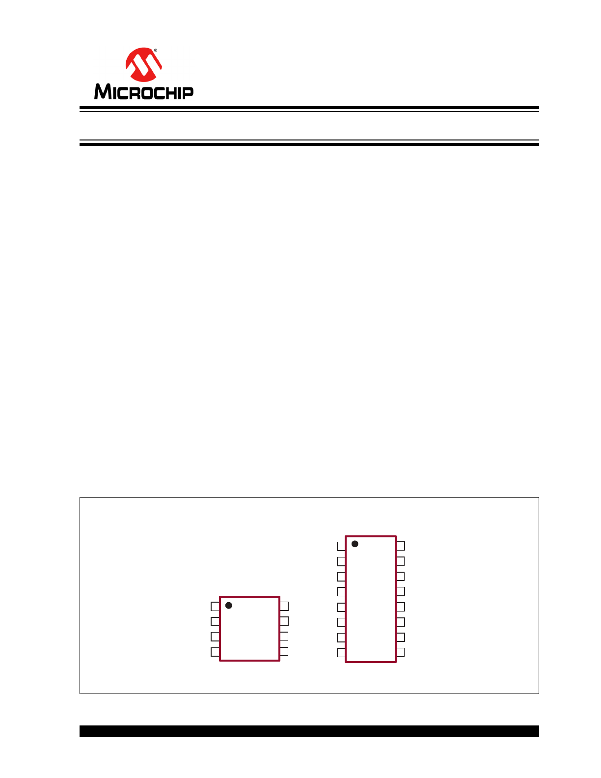
Package Type
16-lead SOIC
(Top view)
1
2
3
4
5
6
7
8
16
15
14
13
12
11
10
9
8
7
6
5
1
2
3
4
VIN
CS
GND
GATE
RT
LD
VDD
PWMD
VIN
NC
NC
CS
GND
NC
NC
GATE
NC
NC
RT
LD
VDD
NC
NC
PWMD
8-lead SOIC
(Top view)
See
Table 2-1
for pin information.
s
LED Driver with Average-Current Mode Constant-Current Control
HV9961
DS20005588A-page 2
2017 Microchip Technology Inc.
Functional Block Diagram
CS
R
S
Q
Q
T
OFF
Timer
L/E
Blanking
GATE
0.44V
MIN (V
LD
• 0.185, 0.275V)
LD
400µs
PWMD
RT
GND
Current
Mirror
i
Regulator
VIN
VDD
UVLO
POR
0.15/0.20V
Average Current
Control Logic
OUT
Auto-REF
HV9961
CLK
IN
Hiccup
2017 Microchip Technology Inc.
DS20005588A-page 3
HV9961
Typical Application Circuit
1
4
2
8
5
6
7
3
HV9961
VIN
GATE
PWMD
LD
VDD
RT
CS
GND
LED
Load
Sets
LED
Current
8V–450V
R
CS
R
T
HV9961
DS20005588A-page 4
2017 Microchip Technology Inc.
1.0
ELECTRICAL CHARACTERISTICS
Absolute Maximum Ratings†
V
IN
to GND ............................................................................................................................................ –0.5V to +470V
V
DD
to GND ............................................................................................................................................................ +12V
CS, LD, PWMD, Gate, RT to GND.................................................................................................... –0.3V to V
DD
+0.3V
Junction Temperature, T
J
.................................................................................................................... –40°C to +150°C
Storage Temperature, T
S
..................................................................................................................... –65°C to +150°C
Continuous Power Dissipation (T
A
= +25°C):
8-lead SOIC ............................................................................................................................................ 650 mW
16-lead SOIC ........................................................................................................................................ 1000 mW
† Notice: Stresses above those listed under “Absolute Maximum Ratings” may cause permanent damage to the
device. This is a stress rating only, and functional operation of the device at those or any other conditions above those
indicated in the operational sections of this specification is not intended. Exposure to maximum rating conditions for
extended periods may affect device reliability.
ELECTRICAL CHARACTERISTICS
Electrical Specifications: T
A
= 25°C, V
IN
= 12V, V
LD
= V
DD
, and V
PWMD
= V
DD
unless otherwise specified.
Parameter
Sym.
Min.
Typ.
Max.
Unit
Conditions
INPUT
Input DC Supply Voltage Range
V
INDC
8
—
450
V
DC input voltage
(
Note 1
and
Note 2
)
Shutdown Mode Supply Current
I
INSD
—
0.5
1
mA
Pin PWMD connected to
GND (
Note 2
)
INTERNAL REGULATOR
Internally Regulated Voltage
V
DD
7.25
7.5
7.75
V
V
IN
= 8V, I
DD(EXT)
= 0 mA,
500 pF at gate, R
T
= 226 kΩ
Line Regulation of V
DD
∆V
DD, line
0
—
1
V
V
IN
= 8V–450V,
I
DD(EXT)
= 0 mA,
500 pF at gate, R
T
= 226 kΩ
Load Regulation of V
DD
∆V
DD, load
0
—
100
mV
I
DD(EXT)
= 0 mA–1 mA,
500 pF at gate, R
T
= 226 kΩ
V
DD
Undervoltage Lockout Upper
Threshold
V
UVLO
6.45
6.7
6.95
V
V
IN
rising (
Note 2
)
V
DD
Undervoltage Lockout
Hysteresis
∆V
UVLO
—
500
—
mV
V
IN
falling
Maximum Input Current
(Limited by UVLO)
I
IN, MAX
3.5
—
—
mA
V
IN
= 8V, T
A
= 25°C (
Note 3
)
1.5
—
—
V
IN
= 8V, T
A
= 125°C (
Note 3
)
PWM DIMMING
PWMD Input Low Voltage
V
PWMD(LO)
—
—
0.8
V
V
IN
= 8V–450V (
Note 2
)
PWMD Input High Voltage
V
PWMD(HI)
2.2
—
—
V
V
IN
= 8V–450V (
Note 2
)
PWMD Pull-down Resistance
R
PWMD
50
100
150
kΩ
V
PWMD
= 5V
AVERAGE-CURRENT SENSE LOGIC
Current Sense Reference Voltage
V
CST
268
275
286
mV
V
LD
= 1.5V
LD-to-CS Voltage Ratio
A
V(LD)
0.182 0.185 0.188
—
V
LD
= 1.2V
LD-to-CS Voltage Offset
A
V
x V
LD(OFFSET)
0
—
10
mV
Offset = V
CS
– A
V(LD)
x V
LD
,
V
LD
= 1.2V
Note 1: Also limited by package power dissipation limit, whichever is lower
2: Denotes specifications which apply over the full operating ambient temperature range of
–40°C < T
A
< +125°C
3: Specification is obtained by characterization and is not 100% tested.
2017 Microchip Technology Inc.
DS20005588A-page 5
HV9961
CS Threshold Temperature
Regulation
∆V
CST(TEMP)
—
—
5
mV
(
Note 2
)
LD Input Shutdown Threshold
Voltage
V
LD(OFF)
—
150
—
mV
V
LD
falling
LD Input Enable Threshold Voltage
V
LD(EN)
—
200
—
mV
V
LD
rising
Current Sense Blanking Interval
T
BLANK
150
—
320
ns
(
Note 2
)
Minimum On-time
T
ON(MIN)
—
—
1000
ns
V
CS
= V
CST
+ 30 mV
Maximum Steady-state Duty Cycle
D
MAX
75
—
—
%
Reduction in output LED
current may occur beyond
this duty cycle
SHORT-CIRCUIT PROTECTION
Hiccup Threshold Voltage
V
CSH
410
440
470
mV
Current Limit Delay CS-to-Gate
T
DELAY
—
—
150
ns
V
CS
= V
CSH
+ 30 mV
Short-circuit Hiccup Time
T
HICCUP
350
400
550
μs
Minimum On-time (Short-circuit)
T
ON(MIN),SC
—
—
430
ns
V
CS
= V
DD
T
OFF
TIMER
Off-time
T
OFF
32
40
48
μs
R
T
= 1 MΩ
8
10
12
R
T
= 226 kΩ
GATE DRIVER
Gate Sourcing Current
I
SOURCE
0.165
—
—
A
V
GATE
= 0V, V
DD
= 7.5V
Gate Sinking Current
I
SINK
0.165
—
—
A
V
GATE
= V
DD
, V
DD
= 7.5V
Gate Output Rise Time
t
r
—
30
50
ns
C
GATE
= 500 pF, V
DD
= 7.5V
Gate Output Fall Time
t
f
—
30
50
ns
C
GATE
= 500 pF, V
DD
= 7.5V
TEMPERATURE SPECIFICATIONS
Parameter
Sym.
Min.
Typ.
Max.
Unit
Conditions
TEMPERATURE RANGES
Operating Ambient Temperature
T
A
–40
—
+125
°C
Maximum Junction Temperature
T
J(MAX)
—
—
+150
°C
Storage Temperature
T
S
–65
—
+150
°C
PACKAGE THERMAL RESISTANCE
8-lead SOIC
JA
—
101
—
°C/W
16-lead SOIC
JA
—
83
—
°C/W
ELECTRICAL CHARACTERISTICS (CONTINUED)
Electrical Specifications: T
A
= 25°C, V
IN
= 12V, V
LD
= V
DD
, and V
PWMD
= V
DD
unless otherwise specified.
Parameter
Sym.
Min.
Typ.
Max.
Unit
Conditions
Note 1: Also limited by package power dissipation limit, whichever is lower
2: Denotes specifications which apply over the full operating ambient temperature range of
–40°C < T
A
< +125°C
3: Specification is obtained by characterization and is not 100% tested.
HV9961
DS20005588A-page 6
2017 Microchip Technology Inc.
2.0
PIN DESCRIPTION
The details on the pins of HV9961 are listed on
Table 2-1
. Refer to
Package Types
for the location of
pins.
TABLE 2-1:
PIN FUNCTION TABLE
Pin Number
Pin Name
Description
8-lead SOIC 16-lead SOIC
1
1
VIN
This pin is the input of an 8V–450V linear regulator.
2
4
CS
This pin is the current sense pin used to sense the FET current with
an external sense resistor.
3
5
GND
Ground return for all internal circuitry. This pin must be electrically
connected to the ground of the power train.
4
8
Gate
This pin is the output of gate driver for driving an external N-chan-
nel power MOSFET.
5
9
PWMD
This is the PWM dimming input of the IC. When this pin is pulled to
GND, the gate driver is turned off. When the pin is pulled high, the
gate driver operates normally.
6
12
V
DD
This is the power supply pin for all internal circuits. It must be
bypassed with a low ESR capacitor to GND (at least 0.1 μF).
7
13
LD
This pin is the linear dimming input, and it sets the current sense
threshold as long as the voltage at this pin is less than 1.5V. If volt-
age at LD falls below 150 mV, the gate output is disabled. The gate
signal recovers at 200 mV at LD.
8
14
RT
A resistor connected between this pin and GND programs the gate
off-time.
—
2, 3, 6, 7, 10,
11, 15 and16
NC
No connection
2017 Microchip Technology Inc.
DS20005588A-page 7
HV9961
3.0
APPLICATION INFORMATION
3.1
General Description
Peak current control (as in HV9910B) is the simplest
and the most economical way to regulate a buck
converter's output current. However, it suffers accuracy
and regulation problems that arise from
peak-to-average current error, contributed by the
current ripple in the output inductor and the
propagation delay in the current sense comparator.
The full inductor current signal is unavailable for direct
switch current sensing across the sense resistor at the
ground path in this low-side switch buck converter
when the control switch is at the ground potential
because the switch is turned off. While it is very simple
to detect the peak current in the switch, controlling the
average inductor current is usually implemented by
level translating the sense signal from +V
IN
. Although
this is practical for a relatively low-input voltage, V
IN
,
this type of average-current control may become
excessively complex and expensive in the offline AC or
other high-voltage DC applications.
The HV9961 uses a proprietary control scheme that
allows fast and accurate control of the average current
in the buck inductor by sensing the switch current only.
No compensation of the current control loop is
required. The output LED current’s response to PWMD
input is similar to that of the HV9910B. The effect of
inductor current ripple amplitude on this control
scheme is insignificant. Therefore, the LED current is
independent of the variation in inductance, switching
frequency or output voltage. Constant off-time control
of the buck converter is used for stability and improving
the LED current regulation over a wide range of input
voltages. Unlike HV9910B, the HV9961 does not
support Constant Frequency mode.
3.2
Off Timer
The timing resistor connected between RT and GND
determines the off-time of the gate driver. Wiring this
resistor between RT and Gate as with HV9910B is no
longer supported. Refer to
Equation 3-1
for the
computation of the gate output’s off-time.
EQUATION 3-1:
T
OFF
s
R
T
k
25
------------------- 0.3
+
=
within the range of 30 kΩ ≤ R
T
≤ 1 MΩ
3.3
Average-Current Control
Feedback and Output Short-circuit
Protection
The current through the switching Metal-oxide
Semiconductor Field-effect Transistor (MOSFET)
source is averaged and used to give constant-current
feedback. This current is detected with a sense resistor
at the CS pin. The feedback operates in a fast
Open-loop mode. No compensation is required. Output
current is programmed as seen in
Equation 3-2
.
EQUATION 3-2:
I
LED
0.275V
R
CS
-----------------
=
When the voltage at the LD input V
LD
≥ 1.5V
If the voltage at the LD input is less than 1.5V, the
output current is computed as specified in
Equation 3-3
.
EQUATION 3-3:
I
LED
V
LD
0.185
R
CS
------------------------------
=
When the voltage at the LD input 0.2V ≤ V
LD
< 1.5V
The above equations are only valid for continuous
conduction of the output inductor. It is good design
practice to choose the inductance of the inductor such
that the peak-to-peak inductor current is 30% to 40% of
the average DC full-load current. Hence, the
recommended inductance can be calculated as shown
in
Equation 3-4
.
EQUATION 3-4:
L
O
V
O MAX
T
OFF
0.4 I
O
-----------------------------------------
=
The duty-cycle range of the current control feedback is
limited to D ≤ 0.75. A reduction in the LED current may
occur when the desired LED string voltage V
O
is
greater than 75% of the input voltage V
IN
of the
HV9961 LED driver.
Reducing the targeted output LED string voltage V
O
below V
O(MIN)
= V
IN
x D
MIN
, where D
MIN
= 1 µs/(T
OFF
+1 µs), may also result in the loss of regulation of the
LED current. This condition, however, causes an
increase in the LED current and can potentially trip the
short-circuit protection comparator.
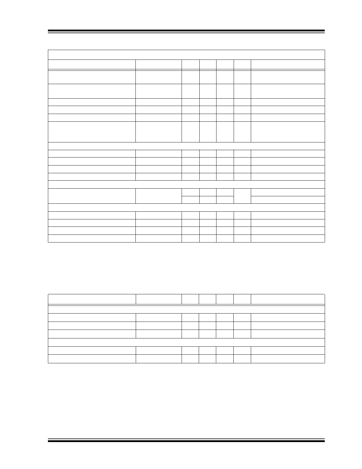
The typical output characteristic of the HV9961 LED
driver is shown in
Figure 3-1
. The corresponding
HV9910B characteristic is given for the comparison.
HV9961
DS20005588A-page 8
2017 Microchip Technology Inc.
FIGURE 3-1:
Typical Output
Characteristic of an HV9961 LED Driver.
V
IN
= 170VDC
HV9961
HV9910B
0 10 20 30 40 50 60
0.60
0.55
0.50
0.45
0.40
0.35
0.30
0.25
LED Current (A)
Output Voltage (V)
Output Characteristics
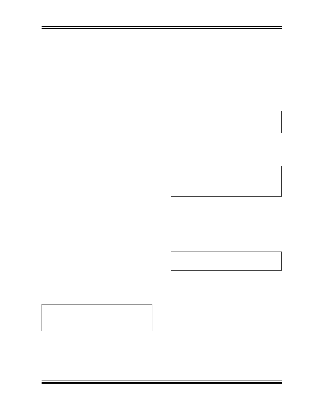
The short-circuit protection comparator trips when the
voltage at CS exceeds 0.44V. When this occurs, the
short-circuit gate off-time T
HICCUP
= 400 µs is
generated to prevent the staircasing of the inductor
current and, potentially, its saturation due to insufficient
output voltage. The typical short-circuit inductor current
is shown in the waveform of
Figure 3-2
.
400µs
0.44V/R
CS
FIGURE 3-2:
Short-circuit Inductor
Current.
A leading-edge blanking delay is provided at CS to
prevent false triggering of the current feedback and the
short-circuit protection.
3.4
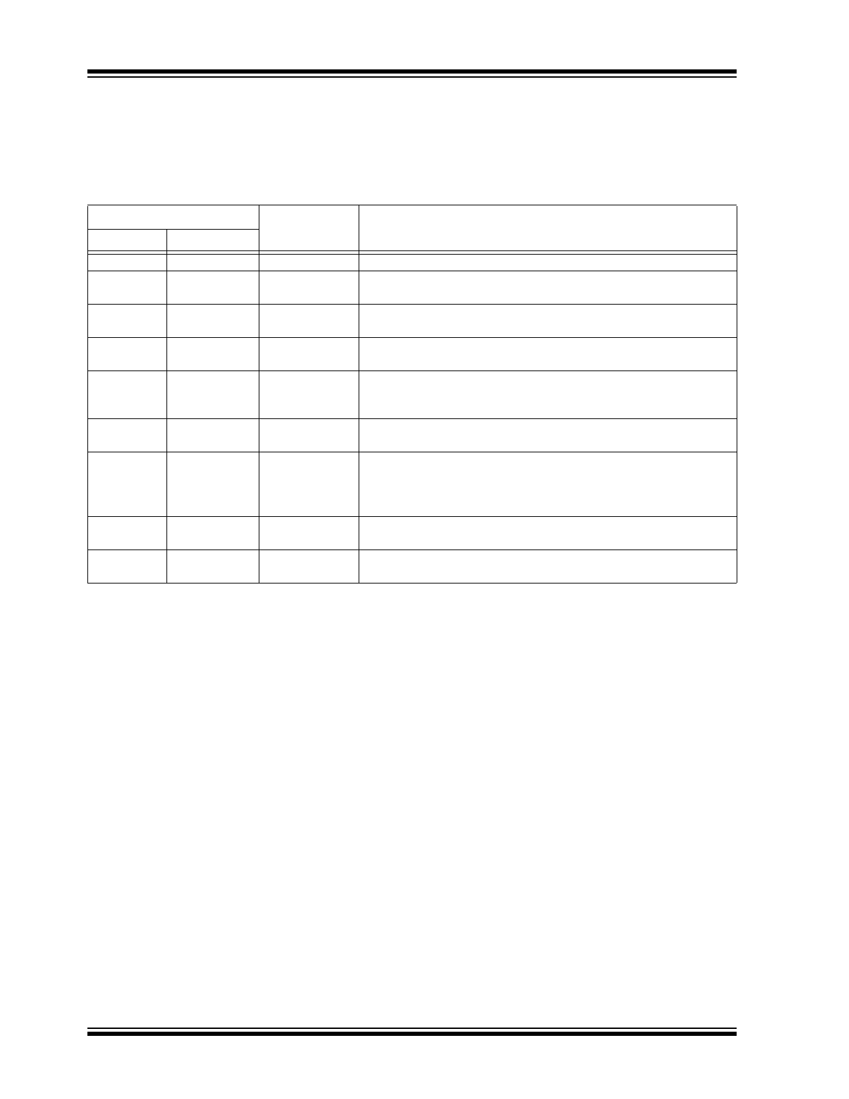
Linear Dimming
When the voltage at LD falls below 1.5V, the internal
275 mV reference to the constant-current feedback
becomes overridden by V
LD
x 0.185. As long as the
current in the inductor remains continuous, the LED
current is given by
Equation 3-3
. However, when V
LD
falls below 150 mV, the gate output becomes disabled.
The gate signal recovers when V
LD
exceeds 200 mV. It
is required in some applications to use the same
brightness control signal input to shut off the lamp. The
typical linear dimming response is shown in
Figure 3-3
.
FIGURE 3-3:
0 0.2 0.4 0.6 0.8 1.0 1.2 1.4 1.6
0.40
0.35
0.30
0.25
0.20
0.15
0.10
0.05
0
LED Current (A)
LD (V)
LD Response Characteristics
Typical Linear Dimming
Response of an HV9961 LED Driver.
The linear dimming input could also be used for
“mixed-mode” dimming to expand the dimming ratio. In
such case, a pulse-width modulated signal with an
amplitude below 1.5V should be applied to LD.
3.5
Input Voltage Regulator
The HV9961 can be powered directly from an
8 V
DC
–450 V
DC
supply through its V
IN
input. When this
voltage is applied at the V
IN
pin, the HV9961 maintains
a constant 7.5V level at V
DD
. This voltage can be used
to power the IC and external circuitry connected to V
DD
within the rated maximum current or within the thermal
ratings of the package, whichever limit is lower. The
V
DD
pin must be bypassed by a low ESR capacitor to
provide a low-impedance path for the high-frequency
current of the gate output. The HV9961 can also be
powered through the V
DD
pin directly with a voltage
greater than the internally regulated 7.5V, but less than
12V.
Despite the instantaneous voltage rating of 450V,
continuous voltage at V
IN
is limited by the power
dissipation in the package. For example, when HV9961
draws I
IN
= 2.5 mA from the V
IN
input, and the 8-pin
SOIC package is used, the maximum continuous
voltage at V
IN
is limited to the value shown in
Equation 3-5
.
EQUATION 3-5:
V
IN MAX
T
J MAX
T
A
–
R
JA
I
IN
--------------------------------
=
396V
=
Where:
Ambient temperature: T
A
= 25°C
Maximum working junction temperature: T
J(MAX)
= 125°C
Junction-to-ambient thermal resistance:
R
θ,JA
= 101°C/W
2017 Microchip Technology Inc.
DS20005588A-page 9
HV9961
In such cases, when it is needed to operate the
HV9961 from a higher voltage, a resistor or a Zener
diode can be added in series with the V
IN
input to divert
some of the power loss from the HV9961. In the above
example, using a 100V Zener diode will allow the circuit
to work up to 490V. The input current drawn from the
V
IN
pin is represented by
Equation 3-6
.
EQUATION 3-6:
I
IN
1mA Q
G
f
S
+
Where:
f
S
= Switching frequency
Q
G
= Gate charge of the external FET (obtained from
the manufacturer’s data sheet)
3.6
Gate Output
The gate output of the HV9961 is used to drive an
external MOSFET. It is recommended that the gate
charge Q
G
of the external MOSFET be less than 25 nC
for switching frequencies ≤100 kHz and less than
15 nC for switching frequencies >100 kHz.
3.7
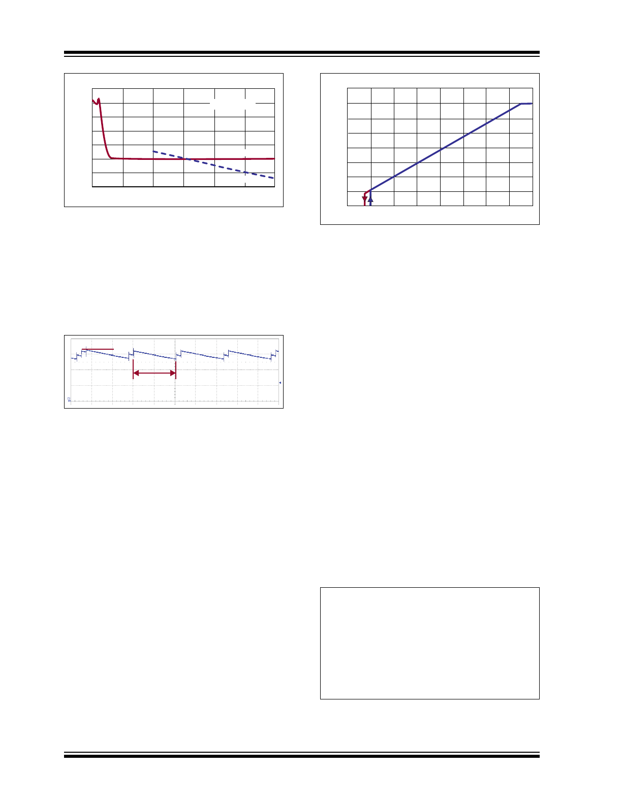
PWM Dimming
Due to the fast open-loop response of the
average-current control loop of the HV9961, its PWM
dimming performance nearly matches that of the
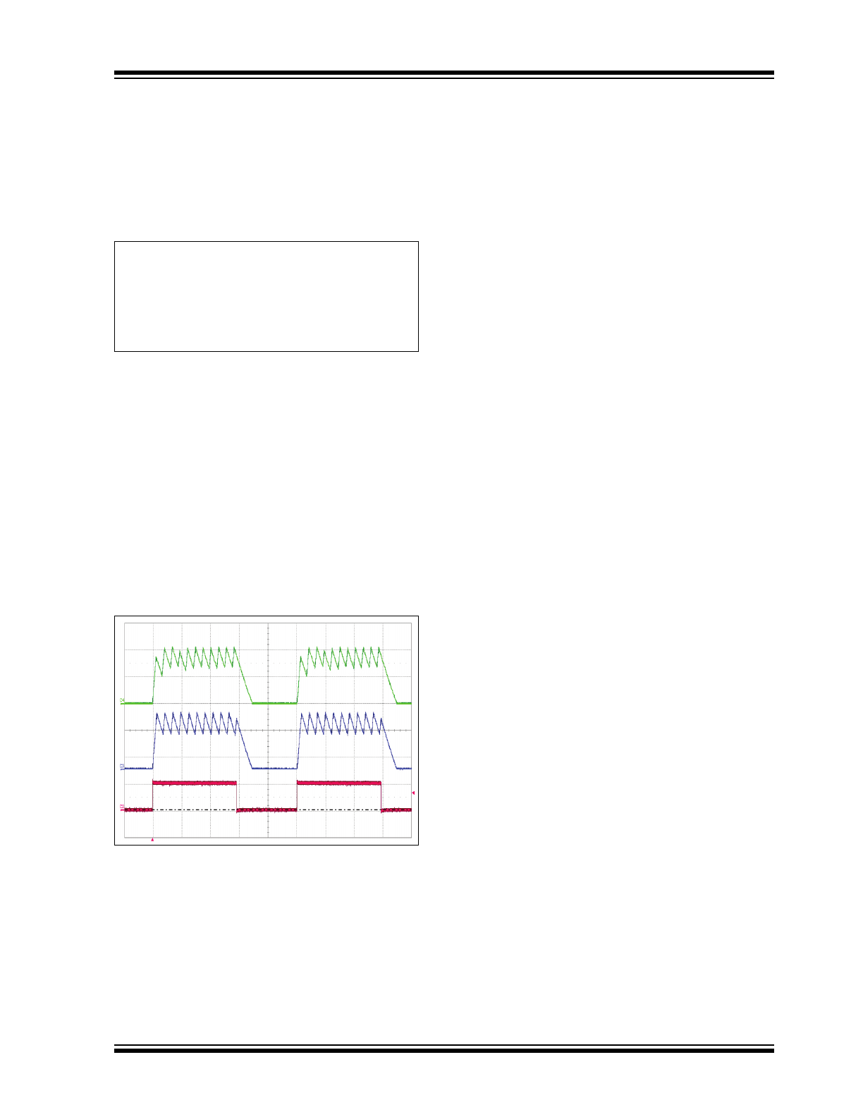
HV9910B. The inductor current waveform comparison
is shown in
Figure 3-4
.
CH4 = Inductor Current
CH3 = Inductor Current
of HV9910B
for comparison
CH2 = V
PWMD
FIGURE 3-4:
Typical PWM Dimming
Response of an HV9961 LED Driver.
The rising and falling edges are limited by the current
slew rate in the inductor. The first switching cycle is
terminated upon reaching the 275 mV or V
LD
x 0.185
level at CS. The circuit is further reaching its
steady-state within 3–4 switching cycles regardless of
the switching frequency.
HV9961
DS20005588A-page 10
2017 Microchip Technology Inc.
4.0
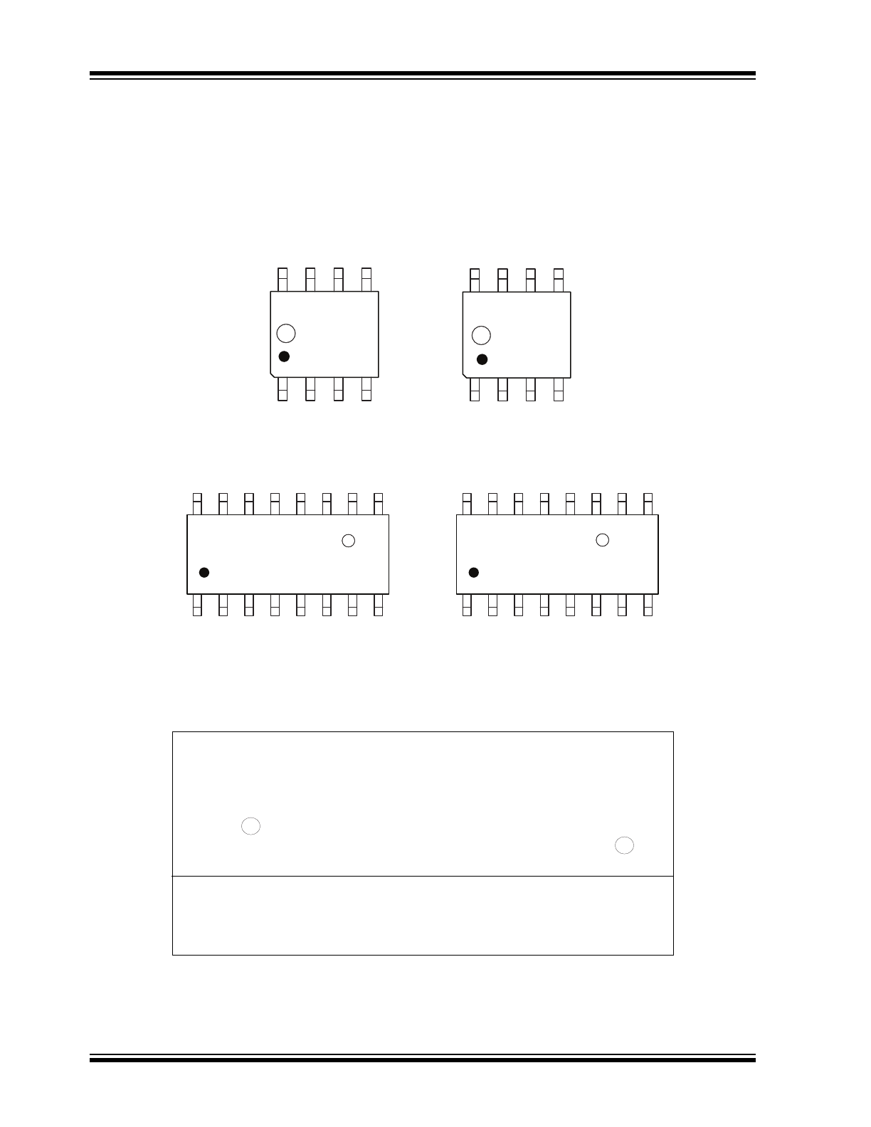
PACKAGING INFORMATION
4.1
Package Marking Information
Legend: XX...X
Product Code or Customer-specific information
Y
Year code (last digit of calendar year)
YY
Year code (last 2 digits of calendar year)
WW
Week code (week of January 1 is week ‘01’)
NNN
Alphanumeric traceability code
Pb-free JEDEC
®
designator for Matte Tin (Sn)
*
This package is Pb-free. The Pb-free JEDEC designator ( )
can be found on the outer packaging for this package.
Note:
In the event the full Microchip part number cannot be marked on one line, it will
be carried over to the next line, thus limiting the number of available
characters for product code or customer-specific information. Package may or
not include the corporate logo.
3
e
3
e
8-lead SOIC
Example
NNN
XXXXXXXX
YYWW
e3
888
HV9961LG
1725
e3
16-lead SOIC
XXXXXXXXX
YYWWNNN
Example
HV9961NG
1714789
e3
e3