
2016 Microchip Technology Inc.
DS20005583A-page 1
HV9912
Features
• Switch-mode Controller for Single-switch Drivers:
- Buck
- Boost
- Buck-boost
- SEPIC
• Works with High-side Current Sensors
• Closed-loop Control of Output Current
• High Pulse-Width Modulation (PWM) Dimming
Ratio
• Internal 90V Linear Regulator (can be extended
using external Zener Diodes)
• Internal 2% Voltage Reference (0°C < T
A
< 85°C)
• Constant Frequency or Constant Off-time
Operation
• Programmable Slope Compensation
• Linear and PWM Dimming
• +0.2A/–0.4A Gate Driver
• Hiccup Mode Protection for both Short-circuit and
Open-circuit Conditions
• Output Overvoltage Protection
• Synchronization Capability
• Pin Compatible with HV9911
Applications
• RGB Backlight Applications
• General LED Lighting Applications
• Battery-powered LED Lamps
General Description
HV9912 is an LED driver IC designed to control
single-switch PWM converters (buck, boost,
buck-boost and SEPIC) in a Constant Frequency or
Constant Off-time mode. The controller uses a peak
Current Mode control scheme with programmable
slope compensation and includes an internal
transconductance amplifier to control the output current
in closed loop, enabling high output current accuracy.
In the case of buck and buck-boost converters, the
output current can be sensed using a high-side current
sensor like the HV7800. In the Constant Frequency
mode, multiple HV9912 ICs can be synchronized with
each other or with an external clock, using the SYNC
pin. Programmable MOSFET current limit enables
current limiting during Input Undervoltage and Output
Overload conditions. The IC also includes a 0.2A
source and 0.4A sink gate driver that makes the
HV9912 suitable for high-power applications. An
internal 90V linear regulator powers the IC, eliminating
the need for a separate power supply for the IC. The IC
also provides a FAULT output, which can be used to
disconnect the LEDs in case of a Fault condition using
an external disconnect FET. HV9912 also provides a
TTL-compatible, low-frequency PWM dimming input
that can accept an external control signal with a duty
ratio of 0-100% and a frequency of up to a few kilohertz.
The HV9912 includes hiccup protection from both short
and open circuits, with automatic recovery after the
Fault condition is cleared.
The HV9912 is a pin-compatible replacement for
HV9911. It can be used with existing HV9911 designs,
which have input voltages of less than 90V, by
changing R
OVP1
, R
OVP
, and R
T
.
Package Type
VIN
VDD
GATE
GND
CS
SC
RT
SYNC
FDBK
IREF
COMP
PWMD
OVP
FAULT
REF
CLIM
1
2
3
4
5
6
7
8
9
10
11
12
13
14
15
16
16-lead SOIC
(Top View)
See
Table 2-1
for pin information.
Switch-Mode LED Driver IC with High Current Accuracy
and Hiccup Mode Protection
HV9912
DS20005583A-page 2
2016 Microchip Technology Inc.
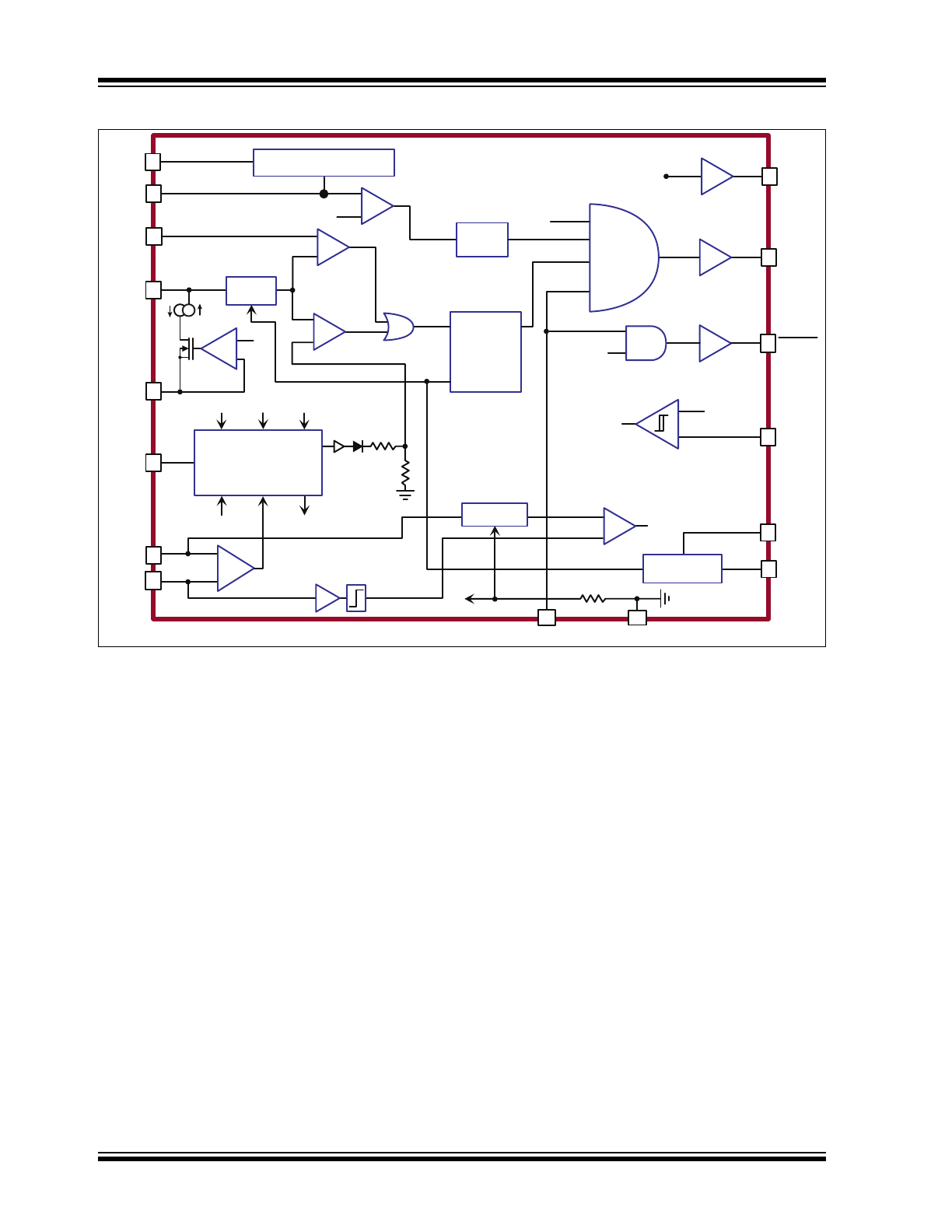
Functional Block Diagram
V
bg
VIN
VDD
REF
GATE
FDBK
IREF
COMP
GND
PWMD
POR
RT
SYNC
S
R
Q
Blanking
CS
SC
ramp
1:2
OVPD
OVP
FAULT
SS
SS
SCD
CLIM
Linear Regulator
One Shot
Hiccup/Dimming
Block
POR
OVD
SCD
PWMD
SS
2
G
M
5V rising
4.5V falling
PWMD
13R
R
5.60/6.10V
T
BLANK
T
BLANK,SC
-
+
+
-
-
+
+
-
+
-
+
-
-
+
2016 Microchip Technology Inc.
DS20005583A-page 3
HV9912
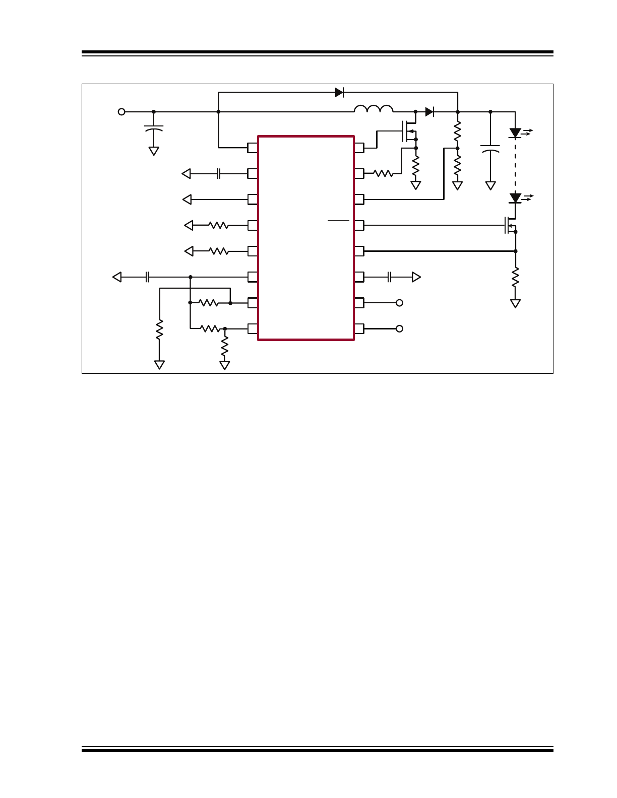
Typical Application Circuit
6
7
10
9
15
8
13
14
16
11
12
5
3
1
2
4
C
IN
C
DD
C
REF
R
R2
R
R1
R
L1
R
L2
R
T
R
SLOPE
R
SC
R
CS
R
OVP1
R
OVP2
C
O
D1
Q1
L1
Q2
C
C
R
S
VIN
VDD
GND
SC
RT
REF
CLIM
IREF
SYNC
PWMD
COMP
FDBK
FAULT
OVP
CS
GATE
HV9912
D2
V
IN
HV9912
DS20005583A-page 4
2016 Microchip Technology Inc.
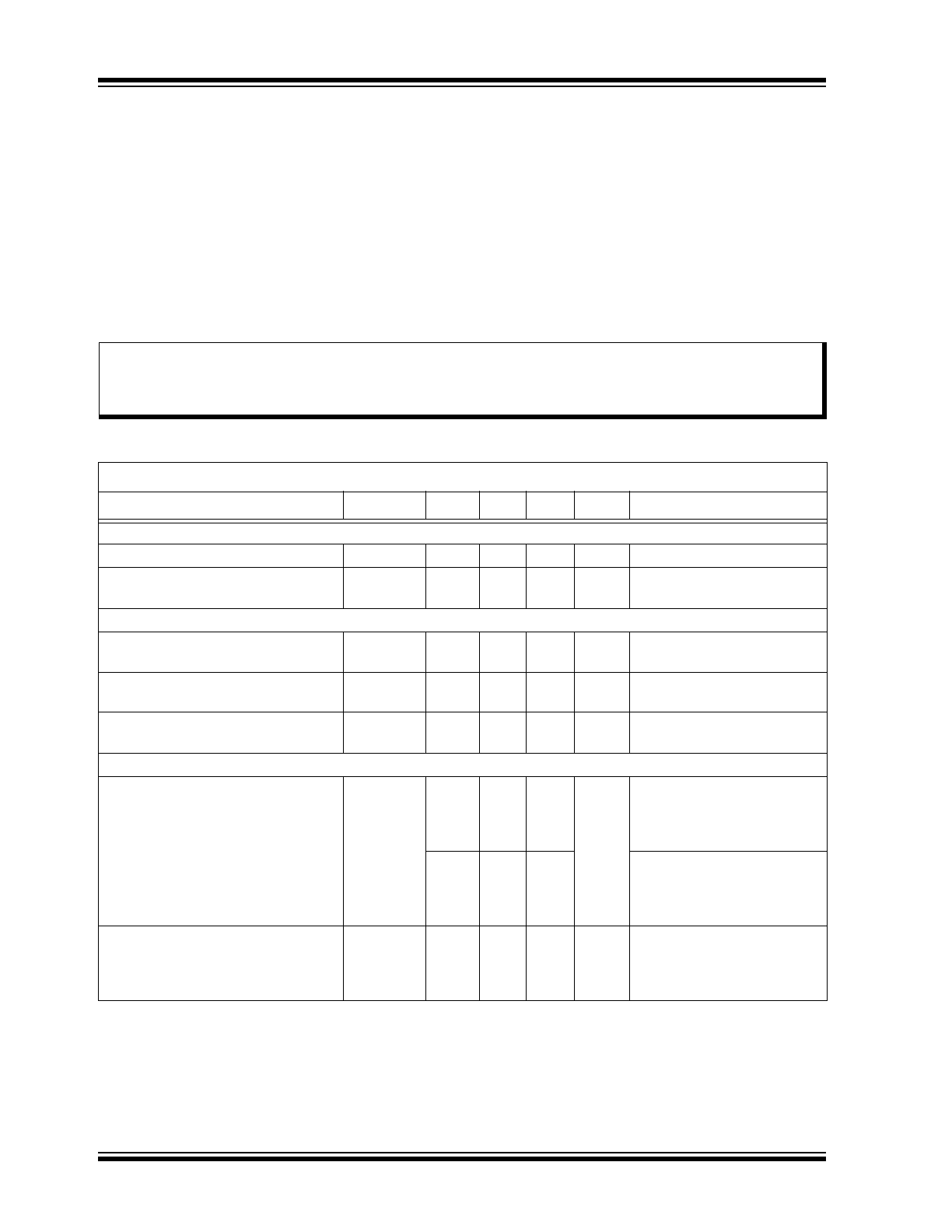
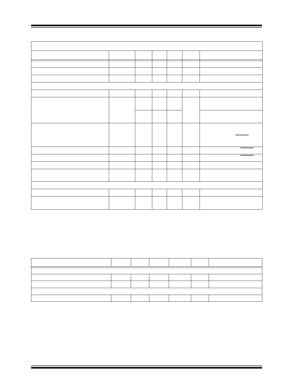
1.0
ELECTRICAL CHARACTERISTICS
Absolute Maximum Ratings †
V
IN
to GND ............................................................................................................................................... –0.5 to +100V
V
DD
to GND............................................................................................................................................–0.3V to +13.5V
CS to GND ........................................................................................................................................ –0.3V to V
DD
+0.3V
PWMD to GND.................................................................................................................................. –0.3V to V
DD
+0.3V
GATE to GND.................................................................................................................................... –0.3V to V
DD
+0.3V
All Other Pins to GND ....................................................................................................................... –0.3V to V
DD
+0.3V
Continuous Power Dissipation (T
A
= +25°C)..................................................................................................... 1200 mW
Operating Junction Temperature Range .............................................................................................. –40°C to +125°C
Storage Temperature Range ................................................................................................................ –65°C to +150°C
† Notice: Stresses above those listed under “Absolute Maximum Ratings” may cause permanent damage to the
device. This is a stress rating only, and functional operation of the device at those or any other conditions above those
indicated in the operational sections of this specification is not intended. Exposure to maximum rating conditions for
extended periods may affect device reliability.
ELECTRICAL CHARACTERISTICS
Electrical Specifications: T
A
= 25°C and V
IN
= 12V unless otherwise specified.
Parameters
Sym.
Min.
Typ.
Max.
Units
Conditions
INPUT
Input DC Supply Voltage Range
V
INDC
Note 1
—
90
V
DC input voltage (
Note 2
)
Shutdown Mode Supply Current
I
INSD
—
—
1.5
mA
PWMD connected to GND
(
Note 2
)
INTERNAL REGULATOR
Internally Regulated Voltage
V
DD
7.25
7.75
8.25
V
V
IN
= 9V–90V; PWMD con-
nected to GND (
Note 2
)
V
DD
Undervoltage Lockout
Threshold
UVLO
RISE
6.5
—
7
V
V
DD
rising
V
DD
Undervoltage Lockout
Hysteresis
UVLO
HYST
—
500
—
mV
V
DD
falling
REFERENCE
REF Pin Voltage
V
REF
1.225
1.25
1.285
V
REF bypassed with a 0.1 µF
capacitor to GND; I
REF
= 0;
PWMD = GND;
0°C < T
A
< +85°C
1.225
1.25
1.29
REF bypassed with a 0.1 µF
capacitor to GND; I
REF
= 0;
PWMD = GND;
–40°C < T
A
< 125°C
Line Regulation of Reference Voltage
V
REFLINE
0
—
20
mV
REF bypassed with a 0.1 µF
capacitor to GND; I
REF
= 0;
V
DD
= 7.25V–12V;
PWMD = GND
Note 1: See
Section 3.3 “Minimum Input Voltage at VIN Pin”
for the minimum input voltage.
2: The specifications which apply over the full operating temperature range at
–40°C < T
A
< +85°C are guaranteed by design and characterization.
3: For design guidance only
2016 Microchip Technology Inc.
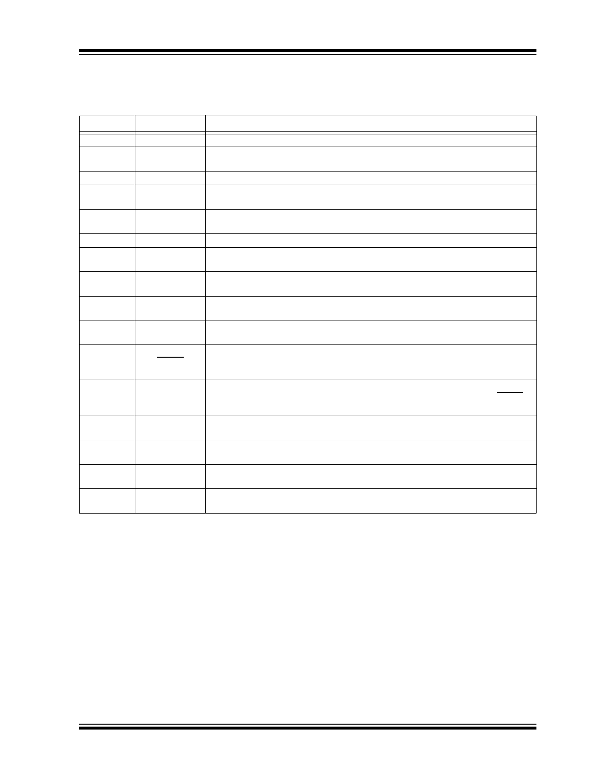
DS20005583A-page 5
HV9912
Load Regulation of Reference
Voltage
V
REFLOAD
0
—
10
mV
REF bypassed with a 0.1 µF
capacitor to GND;
I
REF
= 0 µA–500 µA;
PWMD = GND
PWM DIMMING
PWMD Input Low Voltage
V
PWMD(LO)
—
—
0.8
V
Note 2
PWMD Input High Voltage
V
PWMD(HI)
2
—
—
V
Note 2
PWMD Pull-down Resistance
R
PWMD
50
100
150
kΩ
V
PWMD
= 5V
GATE
GATE Short-circuit Current
I
SOURCE
0.2
—
—
A
V
GATE
= 0V
GATE Sinking Current
I
SINK
0.4
—
—
A
V
GATE
= V
DD
GATE Output Rise Time
T
RISE
—
50
85
ns
C
GATE
= 1 nF
GATE Output Fall Time
T
FALL
—
25
45
ns
C
GATE
= 1 nF
OVERVOLTAGE PROTECTION
Overvoltage Rising Trip Point
V
OVP,RISING
4.75
5
5.25
V
OVP rising
Overvoltage Hysteresis
V
OVP,HYST
—
0.5
—
V
OVP falling
CURRENT SENSE
Leading Edge Blanking
T
BLANK
100
—
280
ns
0°C < T
A
< +85°C
100
—
330
–40°C < T
A
< +125°C
Delay to Output of C
OMP
Comparator
T
DELAY1
—
—
200
ns
COMP = V
DD
; C
LIM
= REF;
C
SENSE
= 0 mV to 600 mV
(step up)
Delay to Output of C
LIMIT
Comparator
T
DELAY2
—
—
200
ns
COMP = V
DD
; C
LIM
= 300 mV;
C
SENSE
= 0 mV to 400 mV
(step up)
Comparator Offset Voltage
V
OFFSET
–10
—
10
mV
INTERNAL TRANSCONDUCTANCE OPAMP
Gain Bandwidth Product
GBW
—
1
—
MHz
75 pF capacitance at OP pin
(
Note 3
)
Open-loop DC Gain
A
V
60
—
—
dB
Output open
Input Common Mode Range
V
CM
–0.3
—
3
V
Note 3
Output Voltage Range
V
O
0.7
—
6.75
V
Note 3
Transconductance
g
M
450
550
650
µA/V
Input Offset Voltage
V
OFFSET
–5
—
5
mV
Input Bias Current
I
BIAS
—
0.5
1
nA
Note 3
OSCILLATOR
Oscillator Frequency
f
OSC1
99
106
118
kHz
R
T
= 500 kΩ (
Note 2
)
f
OSC2
510
580
650
kHz
R
T
= 96 kΩ (
Note 2
)
Maximum Duty Cycle
D
MAX
87
—
93
%
ELECTRICAL CHARACTERISTICS (CONTINUED)
Electrical Specifications: T
A
= 25°C and V
IN
= 12V unless otherwise specified.
Parameters
Sym.
Min.
Typ.
Max.
Units
Conditions
Note 1: See
Section 3.3 “Minimum Input Voltage at VIN Pin”
for the minimum input voltage.
2: The specifications which apply over the full operating temperature range at
–40°C < T
A
< +85°C are guaranteed by design and characterization.
3: For design guidance only
HV9912
DS20005583A-page 6
2016 Microchip Technology Inc.
SYNC Input High
V
SYNCH
2
—
—
V
SYNC Input Low
V
SYNCL
—
—
0.8
V
SYNC Output Current
I
OUTSYNC
—
18
—
µA
OUTPUT SHORT-CIRCUIT
Gain for Short-circuit Comparator
G
SC
1.9
2
2.1
V
Minimum Output Voltage of the Gain
Stage
V
OMIN
0.125
—
0.25
V
0°C < T
A
< +85°C;
I
REF
= GND
0.125
—
0.26
–40°C < T
A
< +125°C;
I
REF
= GND
Propagation Time for Short-circuit
Detection
T
OFF
—
—
250
ns
PWMD = V
DD
; I
REF
= 400 mA;
FDBK step from
0 mV to 900 mV; FAULT goes
from high to low
Fault Output Rise Time
T
RISE,FAULT
—
—
300
ns
330 pF capacitor at FAULT pin
Fault Output Fall Time
T
FALL,FAULT
—
—
300
ns
330 pF capacitor at FAULT pin
Blanking Time
T
BLANK,SC
480
—
900
ns
Current Source at COMP Pin used for
Hiccup Mode Protection
I
HICCUP
—
5
—
µA
SLOPE COMPENSATION
Current Sourced Out of SC Pin
I
SLOPE
0
—
100
µA
Note 2
Internal Current Mirror Ratio
G
SLOPE
1.8
2
2.26
I
SLOPE
= 50 µA;
R
SC
= 1 kΩ
TEMPERATURE SPECIFICATIONS
Parameters
Sym.
Min.
Typ.
Max.
Units
Conditions
TEMPERATURE RANGES
Operating Junction Temperature
T
J
–40
—
+125
°C
Storage Temperature
Ts
–65
—
+150
°C
PACKAGE THERMAL RESISTANCE
16-lead SOIC
JA
—
83
—
°C/W
ELECTRICAL CHARACTERISTICS (CONTINUED)
Electrical Specifications: T
A
= 25°C and V
IN
= 12V unless otherwise specified.
Parameters
Sym.
Min.
Typ.
Max.
Units
Conditions
Note 1: See
Section 3.3 “Minimum Input Voltage at VIN Pin”
for the minimum input voltage.
2: The specifications which apply over the full operating temperature range at
–40°C < T
A
< +85°C are guaranteed by design and characterization.
3: For design guidance only
2016 Microchip Technology Inc.
DS20005583A-page 7
HV9912
2.0
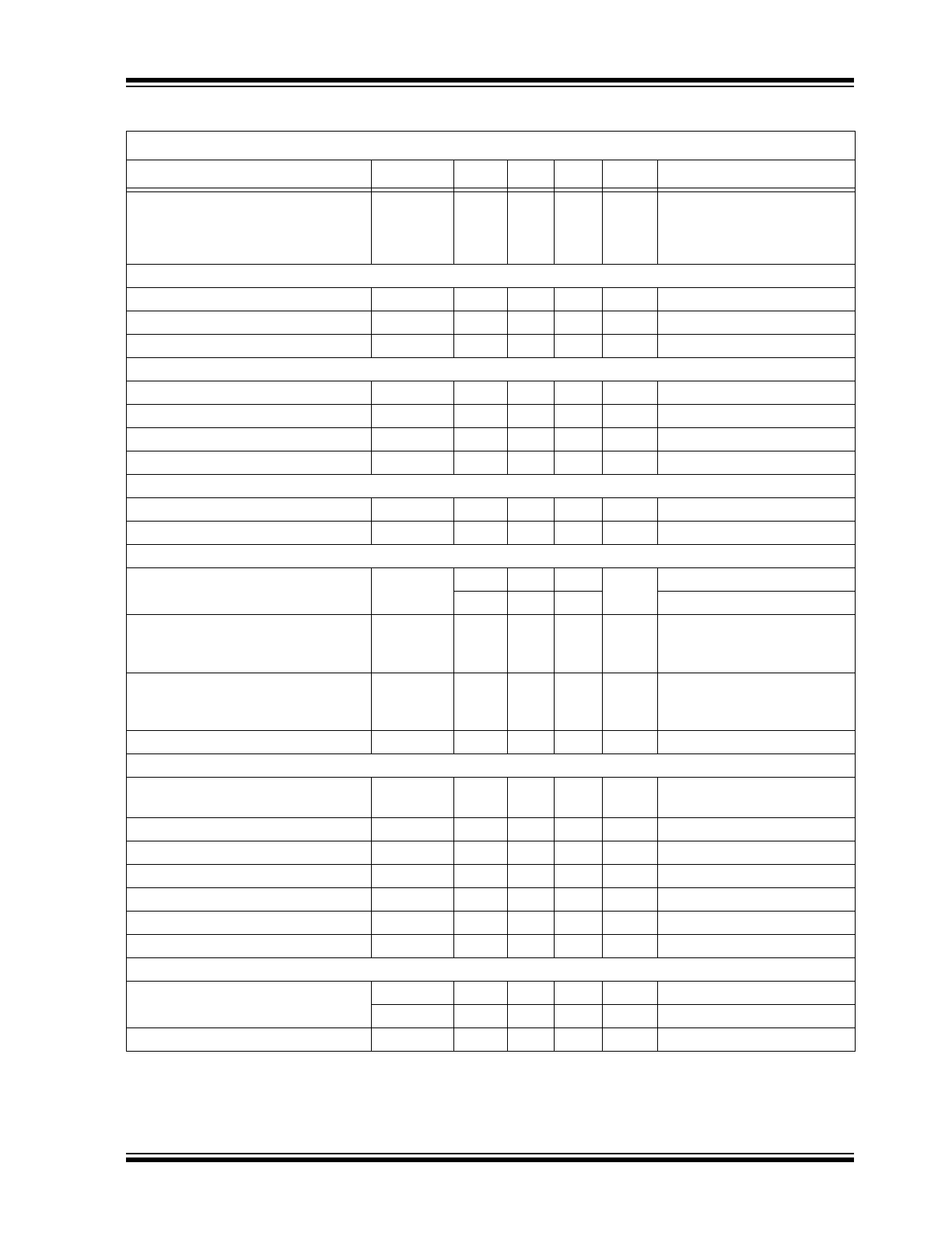
PIN DESCRIPTION
Table 2-1
shows the pin description details of HV9912.
TABLE 2-1:
PIN DESCRIPTION TABLE
Pin Number
Name
Description
1
VIN
This pin is the input of a 90V high-voltage regulator.
2
VDD
This is a power supply pin for all internal circuits. It must be bypassed with a
low-ESR capacitor to GND (at least 0.1 µF).
3
GATE
This pin is the output gate driver for an external N-channel power MOSFET.
4
GND
This is the ground return for all the low-power analog internal circuitry. This pin must
be connected to the return path from the input.
5
CS
This pin is used to sense the source current of the external power FET. It includes a
built-in 100 ns (minimum) blanking time.
6
SC
This pin is used to set the slope compensation.
7
RT
This pin sets the frequency of the power circuit. A resistor between RT and GND will
program the circuit in Constant Frequency mode.
8
SYNC
This I/O pin may be connected to the SYNC pin of other HV9912 circuits and will
cause the oscillators to lock to the highest frequency oscillator.
9
CLIM
This pin provides a programmable input current limit for the converter. The current
limit can be set using a resistor divider from the REF pin.
10
REF
This pin provides 2% accurate reference voltage. It must be bypassed with a
0.01 μF–0.1 μF capacitor to GND.
11
FAULT
This pin is pulled to ground when there is an Output Short-circuit condition or Output
Overvoltage condition. This pin can be used to drive an external MOSFET (in the
case of boost converters) to disconnect the load from the source.
12
OVP
This pin provides the overvoltage protection for the converter. When the voltage at
this pin exceeds 5V, the GATE output of the HV9912 is turned off, and the FAULT
goes low. The IC will turn on when the voltage at the pin goes below 4.5V.
13
PWMD
When this pin is pulled to GND (or left open), switching of the HV9912 is disabled.
When an external TTL high level is applied to it, switching will resume.
14
COMP
Stable Closed-loop control can be accomplished by connecting a compensation net-
work between COMP and GND. This capacitor also controls the hiccup time.
15
IREF
The voltage at this pin sets the output current level. The current reference can be set
using a resistor divider from the REF pin.
16
FDBK
This pin provides output current feedback to the HV9912 by using a current sense
resistor.
HV9912
DS20005583A-page 8
2016 Microchip Technology Inc.
3.0
DETAILED DESCRIPTION
3.1
Power Topology
The HV9912 is a Switch-mode converter LED driver
designed to control a Continuous Conduction mode
buck or boost in a Constant Frequency or Constant
Off-time mode. The IC includes an internal linear
regulator, which operates from input voltages up to
90V, eliminating the need for an external power supply
for the IC. The IC includes features typically required in
LED drivers, such as open LED protection, output
short-circuit protection, linear and PWM dimming,
programmable input current limiting and accurate
control of the LED current. A high-current gate drive
output enables the controller to be used in high-power
converters.
The HV9912 is an enhanced version of the HV9911
with hysteretic overvoltage protection and Hiccup
mode short-circuit protection. The IC includes a
blanking network controlled by the PWMD input to
prevent the short-circuit protection from triggering
prematurely during PWM dimming due to the parasitic
capacitance of the LED string. It also allows the I
REF
pin to be pulled all the way down to GND without
triggering the short-circuit protection. It is a
pin-compatible replacement for the HV9911.
3.2
Linear Regulator
The HV9912 can be powered directly from its V
IN
pin
that withstands a voltage of up to 90V. When a voltage
is applied to the V
IN
pin, the HV9912 tries to maintain a
constant 7.75V (typical) at the V
DD
pin. The regulator
also has a built-in undervoltage lockout which shuts off
the IC if the voltage at the V
DD
pin falls below the UVLO
threshold.
The V
DD
pin must be bypassed by a low-ESR capacitor
(≥0.1 µF) to provide a low-impedance path for the
high-frequency current of the output gate driver.
The input current drawn from the V
IN
pin is the sum of
the 1.5 mA current drawn by the internal circuit and the
current drawn by the gate driver, which in turn depends
on the switching frequency and the gate charge of the
external FET. See
Equation 3-1
.
EQUATION 3-1:
I
IN
1.5mA
Q
G
f
S
+
=
In the above equation, f
S
is the switching frequency,
and Q
G
is the external FET’s gate charge, which can be
obtained from the data sheet of the FET.
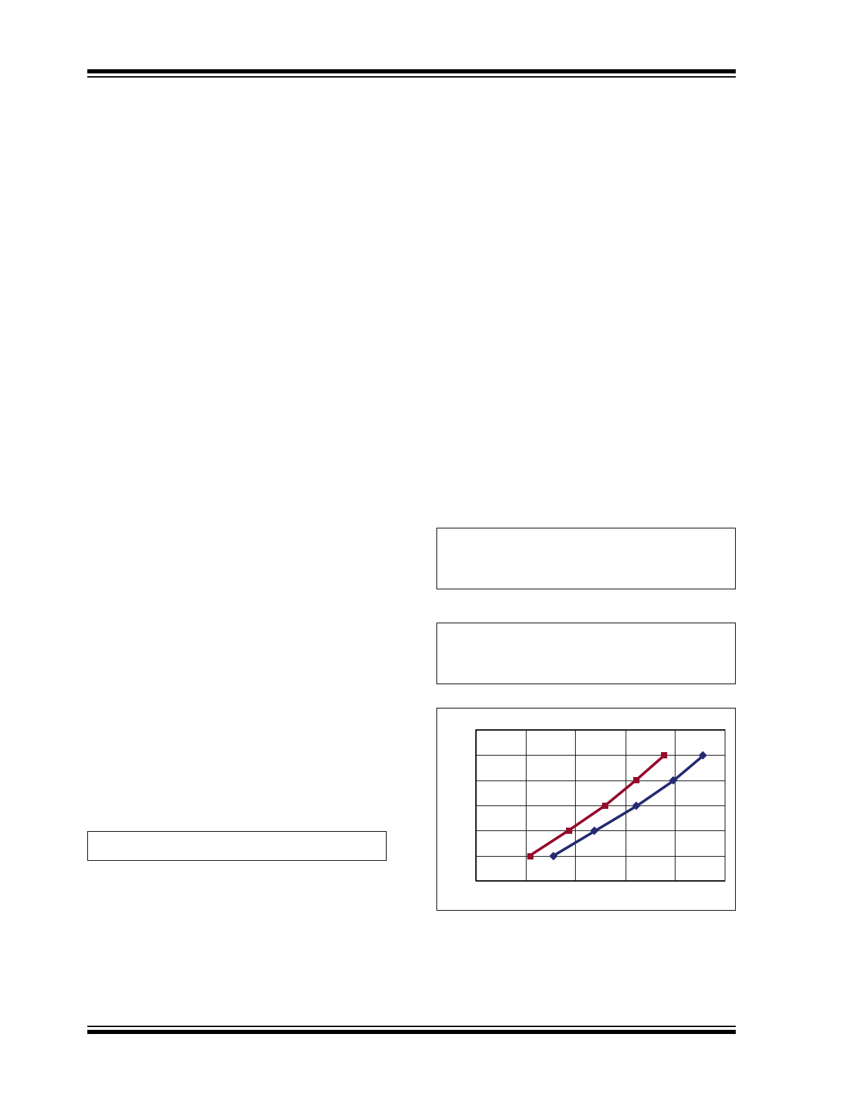
3.3
Minimum Input Voltage at V
IN
Pin
The minimum input voltage at which the converter will
start and stop depends on the minimum voltage drop
required for the linear regulator. The internal linear
regulator will control the voltage at the V
DD
pin when
V
IN
is between 9V and 90V. However, when V
IN
is less
than 9V, the converter will still function as long as V
DD
is greater than the undervoltage lockout. Thus, the
converter might be able to start at input voltages lower
than 9V. The start/stop voltages at the V
IN
pin can be
determined using the minimum voltage drop across the
linear regulator as a function of the current drawn. This
data is shown in
Figure 3-1
for ambient temperatures of
25°C and 85°C.
Assume an ambient temperature of 85°C. Provided
that the IC is driving a 15 nC gate charge FET at
200 kHz, the total input current is estimated to be
4.5 mA when
Equation 3-1
is used. At this input
current, the minimum voltage drop from
Figure 3-1
would be around V
DROP
= 1.25V. However, before the
IC starts switching, the current drawn would have been
1.5 mA. At this current level, the voltage drop would be
approximately V
DROP1
= 0.3V. Thus, the start/stop V
IN
voltages could be computed as demonstrated in
Equation 3-2
and
Equation 3-3
below:
EQUATION 3-2:
V
IN START
UVLO
MAX
V
DROP1
+
=
7V 0.3V
+
=
7.3V
=
EQUATION 3-3:
V
IN STOP
UVLO
MAX
UVLO
–
V
DROP
+
=
7V 0.5V
–
1.25V
+
=
7.75V
=
Minimum Voltage Drop vs. I
IN
0
0.5
1
1.5
2
2.5
3
0 2 4 6 8 10
I
IN
(mA)
M
in
im
u
m V
o
lt
a
g
e D
ro
p (
V
)
T
A
= 25
O
C
T
A
= 85
O
C
FIGURE 3-1:
Headroom vs. Input Current.
In this case, the gate driver draws too much current and
V
INSTART
is less than V
INSTOP
. When this happens, the
IC will oscillate between ON and OFF if the input

2016 Microchip Technology Inc.
DS20005583A-page 9
HV9912
voltage is between the start and stop voltages.
Therefore, it is recommended that the input voltage be
kept higher than V
INSTOP
.
3.4
Reference
HV9912 includes a 2% accurate 1.25V reference,
which can be used as the reference for the output
current as well as to set the switch current limit. The
reference is buffered so that it can deliver a maximum
of 500 µA external current to drive the external circuitry.
The reference should be bypassed with at least a 10 nF
low-ESR capacitor.
Note:
To avoid abnormal Startup conditions, the
bypass capacitor at the REF pin should
not exceed 0.1 µF.
3.5
Oscillator
Connecting the resistor between R
T
and GND will
program the time period.
In both cases, resistor R
T
sets the current, which
charges an internal oscillator capacitor. The capacitor
voltage ramps up linearly. When the voltage increases
beyond the internal set voltage, a comparator triggers
the set input of the internal SR flip-flop. This starts the
next switching cycle. The time period of the oscillator
can be computed as shown in
Equation 3-4
.
EQUATION 3-4:
T
S
R
T
18pF
3.6
Synchronization
The SYNC pin is an input/output (I/O) port to a
fault-tolerant peer-to-peer and/or master clock
synchronization circuit. For synchronization, the SYNC
pins of multiple HV9912-based converters can be
connected together and may also be connected to the
open drain output of a master clock. When connected
in this manner, the oscillators will lock to the device with
the highest operating frequency. When synchronizing
multiple ICs, it is recommended that the same timing
resistor (corresponding to the switching frequency) be
used in all the HV9912 circuits.
On rare occasions, given the length of the connecting
lines for the SYNC pins, a resistor between SYNC and
GND may be required to damp any ringing due to
parasitic capacitances. It is recommended that the
resistor chosen be greater than 300 kΩ.
When synchronized in this manner, a permanent High
or Low condition on the SYNC pin will result in a loss of
synchronization, but the HV9912-based converters will
continue to operate at their individually set operating
frequencies. Since loss of synchronization will not
result in total system failure, the SYNC pin is
considered fault tolerant.
3.7
Slope Compensation
For Continuous Conduction mode converters operating
in the Constant Frequency mode, slope compensation
becomes necessary to ensure stability of the Peak
Current mode controller if the operating duty cycle is
greater than 50%. Choosing a slope compensation
which is one half of the down slope of the inductor
current ensures that the converter will be stable for all
duty cycles.
Slope compensation can be programmed by two
resistors R
SLOPE
and R
SC
. Assuming a down slope of
DS (A/µs) for the inductor current, the slope
compensation resistors can be computed as illustrated
in
Equation 3-5
.
EQUATION 3-5:
R
SC
R
SLOPE
DS 10
6
T
S
R
CS
10
--------------------------------------------------------------------------
=
Where R
CS
is the current sense resistor which
senses the switching FET current
Note:
The maximum current that can be sourced
out of the SC pin is 100 µA. This limits the
minimum value of the R
SLOPE
resistor to
25 kΩ. If the equation for slope
compensation produces a R
SLOPE
less
than this value, then R
SC
would have to be
reduced accordingly. It is recommended
that R
SLOPE
be chosen within the range of
25 kΩ to 50 kΩ.
3.8
Current Sense
The current sense input of the HV9912 includes a
built-in 100 ns (minimum) blanking time to prevent
spurious turn-off due to the initial current spike when
the FET turns on.
The HV9912 includes two high-speed comparators—
one is used during normal operation and the other is
used to limit the maximum input current during Input
Undervoltage or Overload conditions.
The IC includes an internal resistor divider network,
which steps down the voltage at the COMP pin by a
factor of 15. This stepped-down voltage is given to one
of the comparators as the current reference. The
reference to the other comparator, which acts to limit
the maximum inductor current, is given externally.
It is recommended that the sense resistor R
CS
be
chosen so as to provide about 250 mV current sense
signal.
HV9912
DS20005583A-page 10
2016 Microchip Technology Inc.
3.9
Current Limit
Current limit has to be set by a resistor divider from the
1.25V reference available on the IC. Assuming a
maximum operating inductor current I
pk
(including
ripple current), the maximum voltage at the C
LIM
pin
can be set as shown in
Equation 3-6
.
EQUATION 3-6:
V
CLIM
1.2 I
PK
R
CS
5 R
CS
R
SLOPE
+
0.9
Note that this equation assumes a current limit at 120%
of the maximum input current. Also, if V
CLIM
is greater
than 450 mV, the saturation of the internal opamp will
determine the limit on the input current rather than the
C
LIM
pin. In such a case, the sense resistor R
CS
should
be reduced until V
CLIM
reduces below 550 mV.
It is recommended that no capacitor be connected
between C
LIM
and GND.
3.10
Internal 1 MHz Transconductance
Amplifier
HV9912 includes a built-in 1 MHz transconductance
amplifier with tri-state output, which can be used to
close the feedback loop. The output current sense
signal is connected to the FDBK pin and the current
reference is connected to the I
REF
pin.
The output of the opamp is controlled by the signal
applied to the PWMD pin. When PWMD is high, the
output of the opamp is connected to the COMP pin.
When PWMD is low, the output is left open. This
enables the integrating capacitor to hold the charge
when the PWMD signal has turned off the gate drive.
When the IC is enabled, the voltage on the integrating
capacitor will force the converter into Steady state
almost instantaneously.
The output of the opamp is buffered and connected to
the current sense comparator using a 15:1 divider. The
buffer helps to prevent the integrator capacitor from
discharging during the PWM Dimming state.
3.11
PWM Dimming
PWM dimming can be achieved by driving the PWMD
pin with a TTL-compatible square wave source. The
PWM signal is connected internally to three different
nodes—the transconductance amplifier, the FAULT
output and the GATE output.
When the PWMD signal is high, the GATE and FAULT
pins are enabled and the transconductance opamp’s
output is connected to the external compensation
network. Thus, the internal amplifier controls the output
current. When the PWMD signal goes low, the output of
the transconductance amplifier is disconnected from
the compensation network. Therefore the integrating
capacitor maintains the voltage across it. The GATE is
disabled, so the converter stops switching and the
FAULT pin goes low, turning off the disconnect switch.
The output capacitor of the converter determines the
converter’s PWM dimming response because the
capacitor has to get charged and discharged whenever
the PWMD signal goes high or low. In the case of a
buck converter, since the inductor current is
continuous, a very small capacitor is used across the
LEDs. This minimizes the effect of the capacitor on the
converter’s PWM dimming response. However, in the
case of a boost converter, the output current is
discontinuous, and a very large output capacitor is
required to reduce the ripple in the LED current. Thus,
this capacitor will have a significant impact on the PWM
dimming response. By turning off the disconnect switch
when PWMD goes low, the output capacitor is
prevented from being discharged. This dramatically
improves the boost converter’s PWM dimming
response.
Note:
In case of Continuous Conduction mode
boost converters, disconnecting the
capacitor might cause a sudden spike in
the capacitor voltage as the energy in the
inductor is dumped into the capacitor. This
increase in the capacitor voltage might
cause the OVP comparator to trip if the
OVP point is set too close to the maximum
operating voltage. Thus, either the capac-
itor has to be larger to absorb this energy
without increasing the capacitor voltage
significantly or the OVP set point has to be
increased.
3.12
False Triggering of the
Short-Circuit Comparator During
PWM Dimming
During PWM dimming, the parasitic capacitance of the
LED string causes a spike in the output current when
the disconnect FET is turned on. With the HV9911, this
parasitic spike in the output current makes the IC
falsely detect an Overcurrent condition and shut down.
To prevent this false shutdown, an R-C filter is used at
the FDBK pin to filter this spike.
To prevent false triggering in the HV9912, there is a
built-in 500 ns blanking network for the short-circuit
comparator, which eliminates the need for the external
R-C low-pass filter. This blanking network is activated
when the PWMD input goes high. Thus, the
short-circuit comparator will not see the spike in the
LED current during the PWM Dimming turn-on
transition. Once the blanking timer is completed, the
short-circuit comparator will start monitoring the output
current. Thus, the total delay time for detecting a
short-circuit will depend on the condition of the PWMD
input.