
2017 Microchip Technology Inc.
DS20005580A-page 1
HV9911
Features
• Switch-mode Controller for Single-switch Drivers:
- Buck
- Boost
- Buck-boost
- SEPIC
• Works with High-side Current Sensing
• Closed-loop Control of Output Current
• High Pulse-Width Modulation (PWM) Dimming
Ratio
• Internal 250V Linear Regulator (can be extended
using external Zener Diodes)
• Internal 2% Voltage Reference (0°C < T
A
< 85°C)
• Constant Frequency or Constant Off-time
Operation
• Programmable Slope Compensation
• Logic Input for Enable and PWM Dimming
• +0.2A/-0.4A Gate Driver
• Output Short-circuit Protection
• Output Overvoltage Protection
• Synchronization Capability
• Programmable Metal-Oxide Semiconductor
Field-Effect Transistor (MOSFET) Current Limit
Applications
• RGB Backlight Applications
• Battery-powered LED Lamps
• Other DC/DC LED Drivers
General Description
The HV9911 is an LED driver IC designed to control
single-switch PWM converters (buck, boost,
buck-boost and SEPIC) in a Constant Frequency or
Constant Off-time mode. The controller uses a peak
current control scheme with programmable slope
compensation and includes an internal
transconductance amplifier to control the output current
in closed loop, enabling high output current accuracy.
In the Constant Frequency mode, multiple HV9911s
can be synchronized with each other or with an
external clock using the sync pin. Programmable
MOSFET current limit enables current limiting during
Input Undervoltage and Output Overload conditions.
The IC also includes a 0.2A source and 0.4A sink gate
driver for high-power applications. An internal
9V–250V linear regulator powers the IC, eliminating the
need for a separate power supply. The HV9911
provides a TTL-compatible PWM dimming input that
can accept an external control signal with a duty ratio
of 0%–100% and a frequency of up to a few kilohertz.
The IC also provides a FAULT output which, can be
used to disconnect the LEDs in case of a Fault
condition, using an external disconnect FET.
The HV9911-based LED driver is ideal for RGB
backlight applications with DC inputs. HV9911-based
LED lamp drivers can achieve efficiency in excess of
90% for buck and boost applications.
Package Type
VIN
VDD
GATE
GND
CS
SC
RT
SYNC
FDBK
IREF
COMP
PWMD
OVP
FAULT
REF
CLIM
1
2
3
4
5
6
7
8
9
10
11
12
13
14
15
16
16-lead SOIC
(Top view)
See
Table 2-1
for pin information.
Switch-Mode LED Driver IC with High Current Accuracy
HV9911
DS20005580A-page 2
2017 Microchip Technology Inc.
Functional Block Diagram
V
bg
VIN
VDD
REF
GATE
+
_
+
_
13R
R
FDBK
IREF
COMP
GND
PWMD
POR
RT
SYNC
S
R
Q
G
m
+
_
CLIM
100ns
Blanking
+
_
2
CS
DIS
SC
+
_
ramp
1:2
DIS
+
_
V
BG
OVP
R
S
Q
FAULT
POR
DIS
Q
One Shot
Linear
Regulator
2017 Microchip Technology Inc.
DS20005580A-page 3
HV9911
Typical Application Circuit
6
7
10
9
15
8
13
14
16
11
12
5
3
1
2
4
C
IN
C
DD
C
REF
R
R2
R
R1
R
L1
R
L2
R
T
R
SLOPE
R
SC
SC
R
CS
R
OVP1
R
OVP2
C
O
D1
Q1
L1
Q2
C
C
R
S
VIN
VDD
GND
SC
RT
REF
CLIM
IREF
SYNC
PWMD
COMP
FDBK
FAULT
OVP
CS
GATE
HV9911
(Boost)
Typical Application Circuit
L1
6
7
10
9
15
8
13
16
14
5
3
11
12
1
2
4
CC
C
IN
C
DD
C
REF
R
R2
R
R1
R
L1
R
L2
R
T
R
SLOPE
R
SC
R
CS
C
O
D1
Q1
R
S
HV7800
VIN
VDD
GND
SC
RT
REF
CLIM
IREF
SYNC
PWMD
COMP
FDBK
FAULT
GATE
CS
OVP
HV9911
(Buck)
HV9911
DS20005580A-page 4
2017 Microchip Technology Inc.
Typical Application Circuit
6
7
10
9
15
8
13
14
16
11
12
5
3
1
2
4
C
IN
C
DD
C
REF
R
R2
R
R1
R
L1
R
L2
R
T
R
SLOPE
R
SC
R
CS
R
OVP1
R
OVP2
C
O
D1
Q1
L1
Q2
C
C
R
S
L2
C1
VIN
VDD
GND
SC
RT
REF
CLIM
IREF
SYNC
PWMD
COMP
FDBK
FAULT
OVP
CS
GATE
HV9911
(SEPIC)
2017 Microchip Technology Inc.
DS20005580A-page 5
HV9911
1.0
ELECTRICAL CHARACTERISTICS
Absolute Maximum Ratings †
V
IN
to GND................................................................................................................................................ –0.5 to +250V
V
DD
to GND............................................................................................................................................–0.3V to +13.5V
CS to GND ...................................................................................................................................... –0.3V to (V
DD
+0.3V)
PWMD to GND................................................................................................................................ –0.3V to (V
DD
+0.3V)
Gate to GND ................................................................................................................................... –0.3V to (V
DD
+0.3V)
All Other Pins to GND ..................................................................................................................... –0.3V to (V
DD
+0.3V)
Continuous Power Dissipation (T
A
= +25°C; Derate 10 mW/°C above +25°C) ................................................ 1000 mW
Operating Ambient Temperature, T
A
.......................................................................................................–40°C to +85°C
Maximum Junction Temperature, T
J(MAX)
...........................................................................................................+125°C
Storage Temperature, T
S
......................................................................................................................–65°C to +150°C
† Notice: Stresses above those listed under “Absolute Maximum Ratings” may cause permanent damage to the
device. This is a stress rating only, and functional operation of the device at those or any other conditions above those
indicated in the operational sections of this specification is not intended. Exposure to maximum rating conditions for
extended periods may affect device reliability.
ELECTRICAL CHARACTERISTICS
Electrical Specifications: T
A
= 25°C and V
IN
= 24V unless otherwise specified.
Parameter
Sym.
Min.
Typ.
Max.
Unit
Conditions
INPUT
Input DC Supply Voltage Range
V
INDC
Note 2
—
250
V
DC input voltage (
Note 1
)
Shutdown Mode Supply Current
I
INSD
—
1
1.5
mA
PWMD connected to GND,
V
IN
= 24V (
Note 1
)
INTERNAL REGULATOR
Internally Regulated Voltage
V
DD
7.25
7.75
8.25
V
V
IN
= 9V–250V, I
DD(EXT)
= 0,
PWMD connected to GND
(
Note 1
)
V
DD
Undervoltage Lockout
Threshold
UVLO
6.65
6.9
7.2
V
V
DD
Rising
V
DD
Undervoltage Lockout
Hysteresis
∆UVLO
—
500
—
mV
Steady State External Voltage that
can be applied at the V
DD
Pin
V
DD(EXT)
—
—
12
V
Note 3
REFERENCE
REF Pin Voltage
V
REF
1.225
1.25
1.275
V
REF bypassed with a 0.1 µF
capacitor to GND, I
REF
= 0,
V
DD
= 7.75V, PWMD = GND
(
Note 1
)
Line Regulation of Reference
Voltage
V
REFLINE
0
—
20
mV
REF bypassed with a 0.1 µF
capacitor to GND, I
REF
= 0,
V
DD
= 7.25V–12V,
PWMD = GND
Note 1: Denotes specifications which apply over the full operating ambient temperature range of
–40°C < T
A
< +85°C
2: See
Section 3.3 “Minimum Input Voltage at VIN Pin”
for minimum input voltage.
3: Parameters might not be within specifications if the external V
DD
voltage is greater than V
DD(EXT)
or if V
DD
is less than 7.25V.
4: For design guidance only
HV9911
DS20005580A-page 6
2017 Microchip Technology Inc.
Load Regulation of Reference
Voltage
V
REFLOAD
0
—
10
mV
REF bypassed with a 0.1 µF
capacitor to GND,
I
REF
= 0µ–500µ,
PWMD = GND
PMW DIMMING
PWMD Input Low Voltage
V
PWMD(LO)
—
—
0.8
V
V
DD
= 7.25V–12V (
Note 1
)
PWMD Input High Voltage
V
PWMD(HI)
2
—
—
V
V
DD
= 7.25V–12V (
Note 1
)
PWMD Pull-down Resistance
R
PWMD
50
100
150
kΩ
V
PWMD
= 5V
GATE
Gate Short-circuit Current
I
SOURCE
0.2
—
—
A
V
GATE
= 0V, V
DD
= 7.75V
Gate Sinking Current
I
SINK
0.4
—
—
A
V
GATE
= 7.75V, V
DD
= 7.75V
Gate Output Rise Time
T
RISE
—
50
85
ns
C
GATE
= 1 nF, V
DD
= 7.75V
Gate Output Fall Time
T
FALL
—
25
45
ns
C
GATE
= 1 nF, V
DD
= 7.75V
OVERVOLTAGE PROTECTION
IC Shutdown Voltage
V
OVP
1.215
1.25
1.285
V
V
DD
= 7.25V–12V,
OVP rising (
Note 1
)
CURRENT SENSE
Leading Edge Blanking
T
BLANK
100
—
375
ns
Delay to Output of COMP Compara-
tor
T
DELAY1
—
—
180
ns
COMP = V
DD
, C
LIM
= REF,
V
CS
= 0 mV to 600 mV
(step up)
Delay to Output of C
LIMIT
Compara-
tor
T
DELAY2
—
—
180
ns
COMP = V
DD
,
C
LIM
= 300 mV, V
CS
= 0 mV to
400 mV (step up)
Comparator Offset Voltage
V
OFFSET
–10
—
10
mV
INTERNAL TRANSCONDUCTANCE OPAMP
Gain Bandwidth Product
GB
—
1
—
MHz
75 pF capacitance at COMP
pin (
Note 4
)
Open-loop DC Gain
A
V
66
—
—
dB
Output open
Input Common Mode Range
V
CM
–0.3
—
3
V
Note 4
Output Voltage Range
V
O
0.7
—
6.75
—
V
DD
= 7.75V (
Note 4
)
Transconductance
g
m
340
435
530
µA/V
Input Offset Voltage
V
OFFSET
–2
—
4
mV
Input Bias Current
I
BIAS
—
0.5
1
nA
Note 4
OSCILLATOR
Oscillator Frequency
f
OSC1
88
100
112
kHz
R
T
= 909 kΩ (
Note 1
)
f
OSC2
308
350
392
kHz
R
T
= 261 kΩ (
Note 1
)
Maximum Duty Cycle
D
MAX
—
90
—
%
Sync Output Current
I
OUTSYNC
—
10
20
µA
Sync Input Current
I
INSYNC
0
—
200
µA
V
SYNC
< 0.1V
ELECTRICAL CHARACTERISTICS (CONTINUED)
Electrical Specifications: T
A
= 25°C and V
IN
= 24V unless otherwise specified.
Parameter
Sym.
Min.
Typ.
Max.
Unit
Conditions
Note 1: Denotes specifications which apply over the full operating ambient temperature range of
–40°C < T
A
< +85°C
2: See
Section 3.3 “Minimum Input Voltage at VIN Pin”
for minimum input voltage.
3: Parameters might not be within specifications if the external V
DD
voltage is greater than V
DD(EXT)
or if V
DD
is less than 7.25V.
4: For design guidance only
2017 Microchip Technology Inc.
DS20005580A-page 7
HV9911
OUTPUT SHORT CIRCUIT
Propagation Time for Short-circuit
Detection
T
OFF
—
—
250
ns
I
REF
= 200 mV,
FDBK = 450 mV, FAULT goes
from high to low
Fault Output Rise Time
T
RISE, FAULT
—
—
300
ns
1 nF capacitor at FAULT pin
Fault Output Fall Time
T
FALL, FAULT
—
—
200
ns
1 nF capacitor at FAULT pin
Amplifier Gain at I
REF
Pin
G
FAULT
1.8
2
2.2
—
I
REF
= 200 mV
SLOPE COMPENSATION
Current sourced out of SC Pin
I
SLOPE
0
—
100
µA
Internal Current Mirror Ratio
G
SLOPE
1.8
2
2.2
—
I
SLOPE
= 50 µA,
RC
SENSE
= 1 kΩ
TEMPERATURE SPECIFICATIONS
Temperature Characteristics: Unless otherwise noted, for all specifications T
A
=T
J
= +25°C.
Parameter
Sym.
Min.
Typ.
Max.
Unit
Conditions
TEMPERATURE RANGE
Operating Ambient Temperature
T
A
–40
—
+85
°C
Maximum Junction Temperature
T
J(MAX)
—
—
+125
°C
Storage Temperature
Ts
–65
—
+150
°C
PACKAGE THERMAL RESISTANCE
16-lead SOIC
JA
—
83
—
°C/W
ELECTRICAL CHARACTERISTICS (CONTINUED)
Electrical Specifications: T
A
= 25°C and V
IN
= 24V unless otherwise specified.
Parameter
Sym.
Min.
Typ.
Max.
Unit
Conditions
Note 1: Denotes specifications which apply over the full operating ambient temperature range of
–40°C < T
A
< +85°C
2: See
Section 3.3 “Minimum Input Voltage at VIN Pin”
for minimum input voltage.
3: Parameters might not be within specifications if the external V
DD
voltage is greater than V
DD(EXT)
or if V
DD
is less than 7.25V.
4: For design guidance only
HV9911
DS20005580A-page 8
2017 Microchip Technology Inc.
2.0
PIN DESCRIPTION
Table 2-1
shows the description of pins in HV9911.
Refer to
Package Type
for the location of pins.
TABLE 2-1:
PIN DESCRIPTION TABLE
Pin Number
Pin Name
Description
1
VIN
This pin is the input of a 250V high-voltage regulator.
2
VDD
This is a power supply pin for all internal circuits. It must be bypassed with a low
ESR capacitor to GND (at least 0.1 uF).
3
Gate
This pin is the output gate driver for an external N-channel power MOSFET.
4
GND
This is the ground return for all circuits. This pin must be connected to the return
path from the input.
5
CS
This pin is used to sense the drain current of the external power FET. It includes a
built-in 100 ns (minimum) blanking time.
6
SC
This is slope compensation for current sense. A resistor between SC and GND will
program the slope compensation. In case of constant Off-time mode of operation,
slope compensation is unnecessary and the pin can be left open.
7
RT
This pin sets the frequency or the off-time of the power circuit. A resistor between
RT and GND will program the circuit in Constant Frequency mode. A resistor
between RT and gate will program the circuit in a constant Off-time mode.
8
Sync
This I/O pin may be connected to the sync pin of other HV9911 circuits and will
cause the oscillators to lock to the highest frequency oscillator.
9
CLIM
This pin provides a programmable input current limit for the converter. The current
limit can be set by using a resistor divider from the REF pin.
10
REF
This pin provides 2% accurate reference voltage. It must be bypassed with at least a
10 nF–0.22 µF capacitor to GND.
11
FAULT
This pin is pulled to ground when there is an Output Short-circuit condition or Output
Overvoltage condition. This pin can be used to drive an external MOSFET in the
case of boost converters to disconnect the load from the source.
12
OVP
This pin provides the overvoltage protection for the converter. When the voltage at
this pin exceeds 1.25V, the gate output of the HV9911 is turned off and FAULT goes
low. The IC will turn on when the power is recycled.
13
PWMD
When this pin is pulled to GND (or left open), switching of the HV9911 is disabled.
When an external TTL high level is applied to it, switching will resume.
14
COMP
Stable closed-loop control can be accomplished by connecting a compensation net-
work between COMP and GND.
15
IREF
The voltage at this pin sets the output current level. The current reference can be set
using a resistor divider from the REF pin.
16
FDBK
This pin provides output current feedback to the HV9911 by using a current sense
resistor.
2017 Microchip Technology Inc.
DS20005580A-page 9
HV9911
3.0
DETAILED DESCRIPTION
3.1
Power Topology
The built-in linear regulator of the HV9911 can operate
up to 250V at the V
IN
pin. The linear regulator provides
an internally regulated voltage of 7.75V (typical) at V
DD
if the input voltage is within 9V to 250V. This voltage is
used to power the IC and also provide the power to
external circuits connected at the V
DD
and V
REF
pins.
This linear regulator can be turned off by overdriving
the V
DD
pin using an external bootstrap circuit at
voltages higher than 8.25V (up to 12V).
In practice, the input voltage range of the IC is limited
by the current drawn by the IC. Thus, it becomes
important to determine the current drawn by the IC to
find out the maximum and minimum operating voltages
at the V
IN
pin. The main component of the current
drawn by the IC is the current drawn by the switching
FET driver at the gate pin. To estimate this current, we
need to know a few parameters of the FET being used
in the design and the switching frequency.
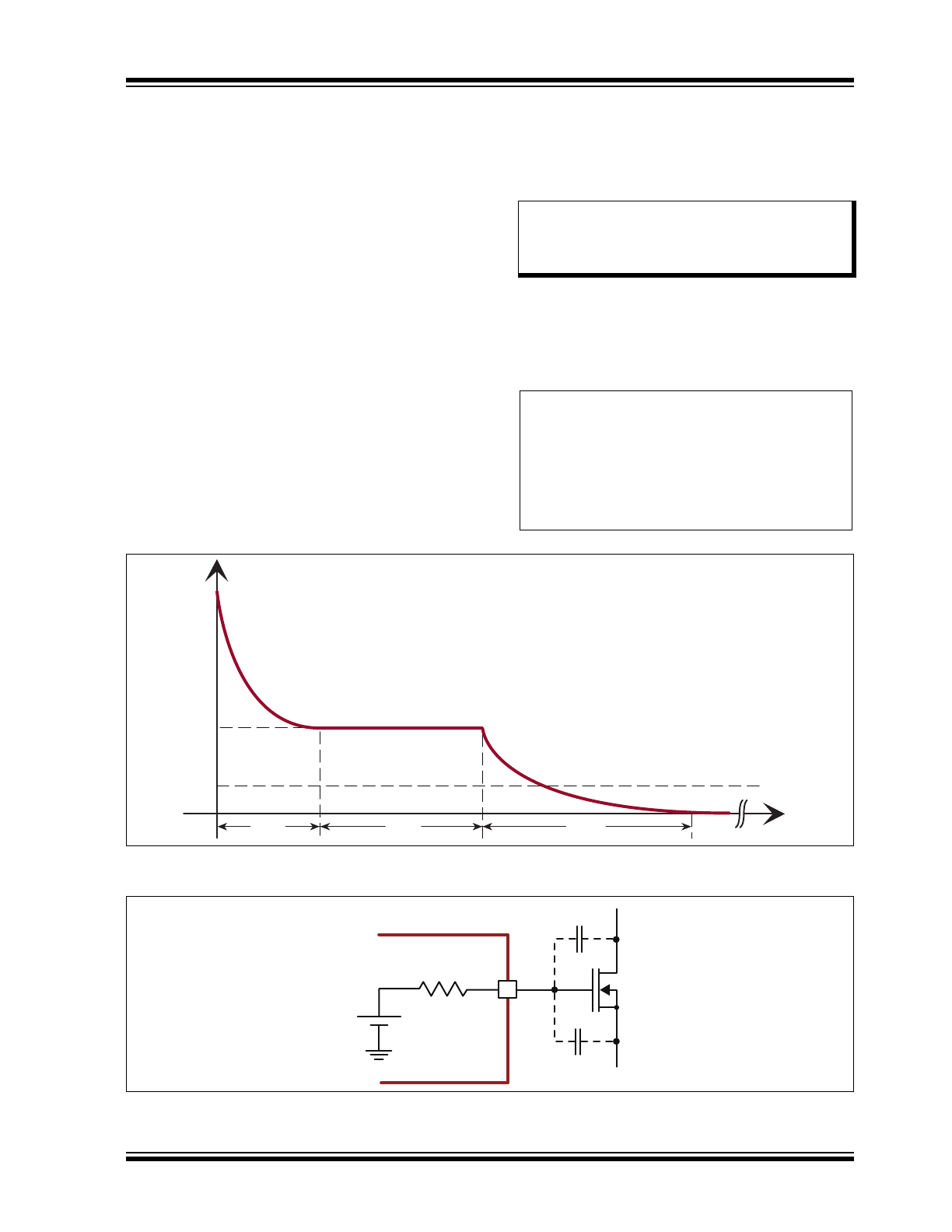
The typical waveform of the current being sourced out
of gate is illustrated in
Figure 3-1
.
Figure 3-2
shows the
equivalent circuit of the gate driver and the external
FET. The values of V
DD
and R
GATE
for the HV9911 are
7.75V and 40Ω, respectively.
Note:
The equations given below are approxima-
tions and are to be used for estimation pur-
poses only. The actual values will likely differ
from the computed values.
Consider the case when the external FET is FDS3692
and the switching frequency is f
S
= 200 kHz with an
LED string voltage V
O
= 80V. With the FET’s
specifications, the following parameters can be
determined:
C
ISS
746pF
=
C
GD
C
RSS
27pF
=
=
C
GS
C
ISS
C
GD
–
=
719pF
=
V
TH
3V
=
I
PK
I
1
I
avg
t
1
t
2
t
3
0
FIGURE 3-1:
Current Sourced Out of Gate at FET Turn-on Driver.
HV9911
C
GD
C
GS
V
DD
R
GATE
FIGURE 3-2:
Equivalent Circuit of the Gate Driver.
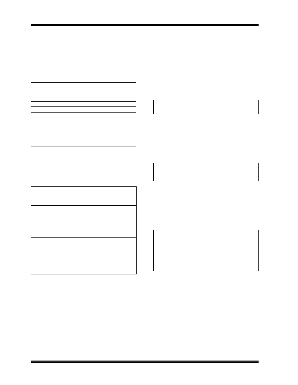
HV9911
DS20005580A-page 10
2017 Microchip Technology Inc.
When the external FET is being turned on, current is
being sourced out of the gate, and that current is being
drawn from the input. Thus, the average current drawn
from V
DD
(and from V
IN
) needs to be computed.
Without going into the details of the FET operation, the
various values in the graph in
Figure 3-1
can be
computed as specified in
Table 3-1
.
TABLE 3-1:
Parameter
Formula
Value
(for a given
example)
I
PK
V
DD
/R
GATE
193.75 mA
I
1
(V
DD
– V
TH
)/R
GATE
118.75 mA
t
1
–R
GATE
x C
ISS
x In (I
1
/I
PK
)
14.61 ns
t
2
[(V
O
– V
TH
) x C
GD
]/I
1
(
1
)
17.5 ns
[(V
IN
– V
TH
) x
GD
]/I
1
(
2
)
t
3
2.3 x R
GATE
x C
GS
66 ns
I
avg
[I
1
x (t
1
+ t
2
) + 0.5 x (I
PK
– I
1
) x
t
1
+ 0.5 x I
1
x t
3
] x f
S
1.66 mA
Note 1:
For a boost converter
2:
For a buck converter
The total current being drawn from the linear regulator
for a typical HV9911 circuit can be computed as shown
in
Table 3-2
.
TABLE 3-2:
Current
Formula
Typical
Value (
2
)
Quiescent Current
1000 µA
1000 µA
Current sourced
out of REF pin
(V
REF
/R
L1
+ R
L2
) +
(V
REF
/R
R1
+ R
R2
)
100 µA
Current sourced
out of RT pin
6V/R
T
13.25 µA
Current sourced
out of SC pin (
1
)
(1/2) x (2.5V/R
SLOPE
)
30.8 µA
Current sourced
out of CS pin (
1
)
2.5V/R
SLOPE
61.6 µA
Current drawn by
FET Gate Driver
I
AVG
1660 µA
Total Current
drawn from the
Linear Regulator
2.865 mA
Note 1:
For a Discontinuous mode converter, the
currents sourced out of the SC and CS pins will
be zero.
2:
The values provided are based on the
Continuous Conduction mode boost design in
the Microchip application note, “AN-H55 Boost
Converter LED Drivers Using the HV9911.”
3.2
Maximum Input Voltage at V
IN
Pin
Computed using the Power
Dissipation Limit
When the regulator is drawing about 2.8 mA, the
maximum input voltage that the HV9911 can withstand
without damage will depend on the ambient
temperature. If we consider an ambient temperature of
40°C, the power dissipation in the package cannot
exceed the P
MAX
in
Equation 3-1
:
EQUATION 3-1:
P
MAX
1000mW 10mW
40
C 25C
–
–
=
850mW
=
The above equation is based on package power
dissipation limits as indicated in the
Absolute
Maximum Ratings †
of this data sheet.
To dissipate a maximum power of 850 mW in the
package, the maximum input voltage cannot exceed
the value in
Equation 3-2
:
EQUATION 3-2:
V
INMAX
P
MAX
I
TOTAL
=
296V
=
Since the maximum voltage is far greater than the
actual input voltage of 24V, power dissipation will not
be a problem for this design.
For this design, at 24V input, the increase in the
junction temperature of the IC (over ambient) is
determined as show in
Equation 3-3
:
EQUATION 3-3:
V
IN
I
TOTAL
ja
=
5.64
C
=
Where:
θ
ja
is the junction to ambient thermal impedance
of HV9911’s 16-lead SOIC package.