
2016 Microchip Technology Inc.
DS20005550A-page 1
Features
• 10V to 450V Input Voltage Range
• Energy-saving Hold Current Mode
• Adjustable Microcontroller Supply
• Low Supply Current <1 mA
• Constant-current Coil Drive
• Programmable Pull-in Current, Pull-in Time and
Hold Current
Applications
• Industrial Controls
• Relay Timers
• Solenoid Drivers
• Home Automation
General Description
The HV9901 universal relay driver provides high-effi-
ciency driving for low-voltage relays with supply volt-
ages as high as 450V. For example, a relay with a 5V
coil can be driven directly from the rectified 120 VAC or
230 VAC line.
The IC includes two high-voltage linear regulators. The
first one is for providing power to internal control cir-
cuitry. The second one has an adjustable output volt-
age and a 1 mA output current capability to support
external circuitry, such as a microcontroller control cir-
cuit.
The pull-in current, pull-in time and hold current for the
relay are individually programmable through two resis-
tors and a capacitor. PWM switching can be synchro-
nized with an external clock or with another HV9901
operating at a higher frequency.
The relay is operated through the enable input ENI.
Logic polarity is under control of the polarity input POL.
Audible noise coming from the relay can be sup-
pressed by operating at a PWM frequency exceeding
20 kHz.
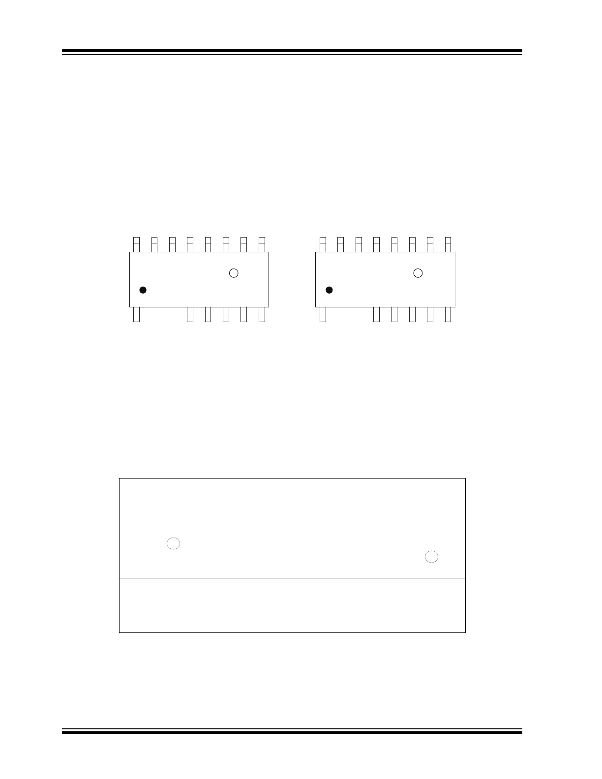
Package Type
1
16
4
16-lead SOIC
See
Table 2-1
for pin information.
WARNING
The HV9901 is suited for relay driving applications operating at hazardous voltage. Ensure that adequate
safeguards are provided to protect the end user from electrical shock.
HV9901
Universal Relay Driver
HV9901
DS20005550A-page 2
2016 Microchip Technology Inc.
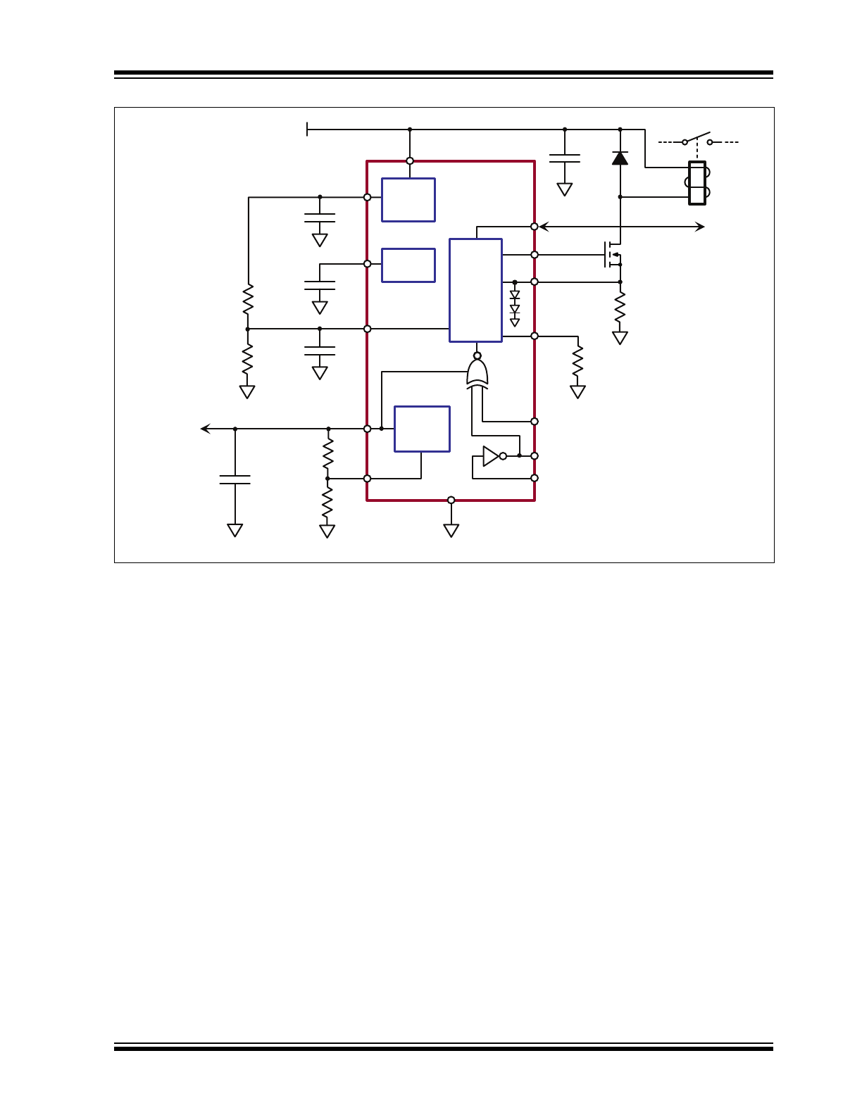
Functional Block Diagram
VIN
A
UVLO
C
VREF
VDD
100 nF
4.7μF
R
S
R
CS
GT
1N4937
RELAY
VN2460N8
LED
10K
1.25V
COM
Q
VDD
Oscillator
shutdown
SYNC
R
OSC
RT
ENI
ENO
POL
VCC
µP
100 nF
5.0V
R
FBA
R
FBB
FB
HOLD/DELAY
R
HDB
R
HDA
5
6
7
8
9
10
11
12
13
14
15
16
C
HD
C
High Limit
Low Limit
VDD
215ns
Delay
Delay
R
2R
1.25V
VDD
High Duty
Cycle
Oscillator
1
VDD
40μA
5.5 kΩ
Bandgap
Reference
+
-
-
+
-
+
-
+
R
S
4
C
HD
2016 Microchip Technology Inc.
DS20005550A-page 3
HV9901
Typical Application Circuit
HV9901
V
IN
SYNC
V
CC
Enable Polarity
Enable
INT
REG
PWM
AUX
REG
V
REF
SYNC
GT
CS
RT
POL
ENO
ENI
VIN
VDD
VREF
H/D
VCC
FB
HV9901
DS20005550A-page 4
2016 Microchip Technology Inc.
1.0
ELECTRICAL CHARACTERISTICS
Absolute Maximum Ratings
†
Input Voltage, V
IN
1
....................................................................................................................................–0.5V to 470V
Input Voltage to any other Pin
1
........................................................................................................ –0.3V to V
DD
+ 0.3V
Operating Junction Temperature Range ................................................................................................ –40°C to +85°C
Continuous Power Dissipation (T
A
= +25°C)
2
.................................................................................................... 750 mW
† Notice: Stresses above those listed under “Maximum Ratings” may cause permanent damage to the device. This is
a stress rating only, and functional operation of the device at those or any other conditions above those indicated in the
operational listings of this specification is not implied. Exposure to maximum rating conditions for extended periods
may affect device reliability.
Note 1: All voltages are referenced to GND.
2: For operation above 25°C ambient, derate linearly at 7.5 mW/°C.
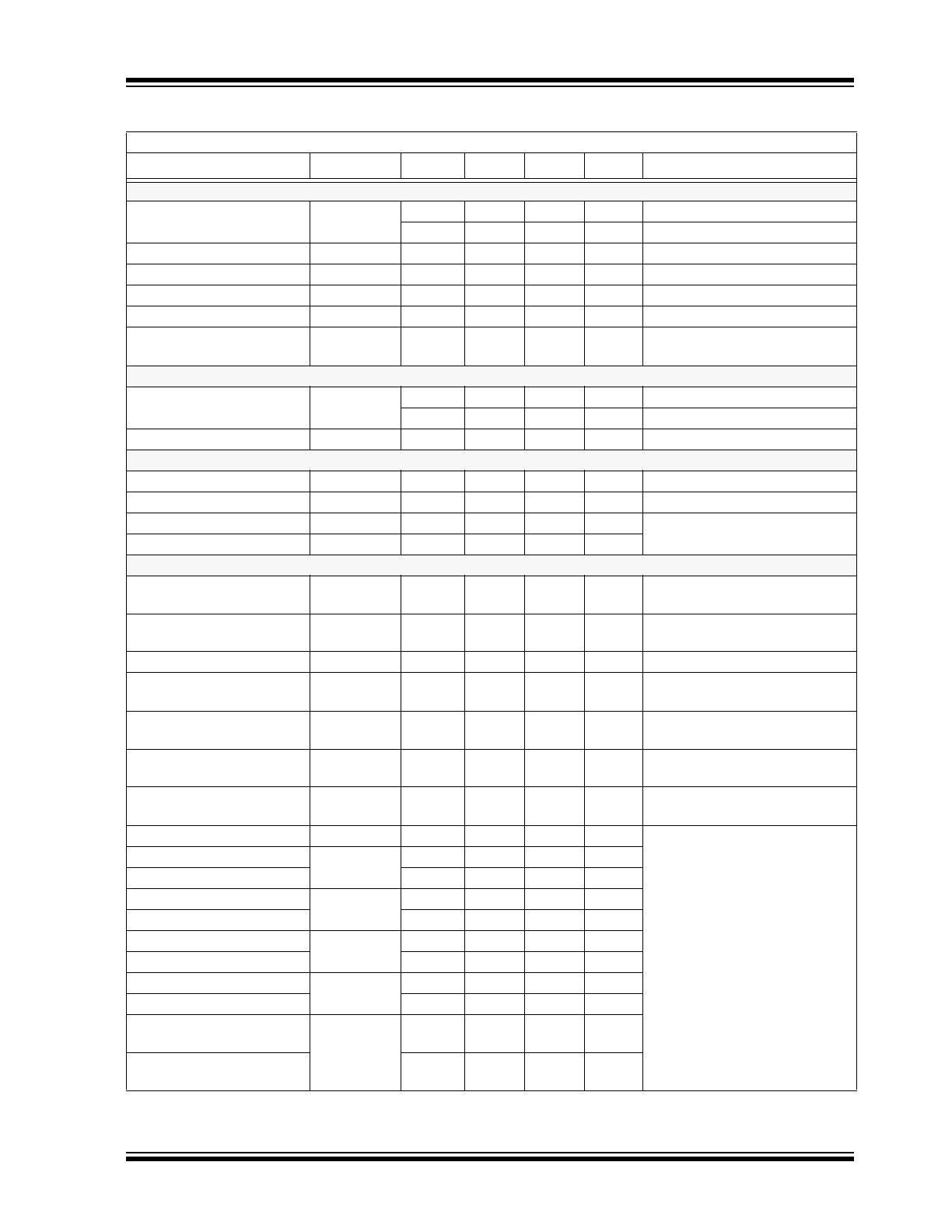
ELECTRICAL CHARACTERISTICS
Electrical Specifications: T
A
= 25°C unless otherwise noted.
Parameter
Symbol
Min.
Typ.
Max.
Unit
Conditions
HIGH-VOLTAGE REGULATOR
Input Voltage
V
IN
10
—
450
V
I
CC
= 0 mA to 1 mA load
Supply Current
I
IN
—
—
2
mA
No load at V
DD
(
Note 1
)
load at I
CC
= 1 mA,
C
GT
= 500 pF, f
OSC
= 25 kHz
Internal Supply Voltage
V
DD
8.5
9
9.5
V
No load at V
DD
(
Note 1
)
C
GT
= 500 pF, f
OSC
= 25 kHz
V
DD
UVLO, On
UVLO
(ON)
7.8
8.2
8.5
V
V
DD
UVLO, Hysteresis
UVLO
(HYST)
—
0.5
—
V
ADJUSTABLE REGULATOR
Regulator Output Voltage
Range
V
CC
2
—
5.5
V
I
CC
= 1 mA load
Regulator Output Current
I
CC
0
—
1
mA
No load at V
DD
(
Note 1
)
Feedback Voltage
V
FB
0
V
REF
V
DD
–1V
V
Input Bias Current
I
FB
—
25
100
nA
V
FB
= V
REF
REFERENCE
Bandgap Reference Voltage
V
REF
1.2
1.25
1.3
V
T
A
= –40°C to +85°C
Load Regulation
—
—
7
mV
0 mA < I
REF
< 0.3 mA
Line Regulation
—
10
15
mV
8.5V < V
DD
< 9.5V
Short Circuit Current
I
REF(SHORT)
—
—
1
mA
Reference Voltage Sink
Current
I
REF(SINK)
—
—
20
μA
2016 Microchip Technology Inc.
DS20005550A-page 5
HV9901
Note 1: Maximum allowable load current limited by power dissipation and operating ambient temperature
OSCILLATOR
PWM Oscillator Frequency
f
OSC
20
25
35
kHz
R
T
= 1 MΩ
80
100
140
kHz
R
T
= 226 kΩ
Temperature Coefficient
—
—
170
—
ppm/°C T
A
= –40°C to +85°C
Oscillator SYNC Frequency
f
SYNC
—
—
150
kHz
SYNC Sourcing Current
I
SYNC
20
—
55
μA
SYNC Sinking Current
I
SYNC
1
—
—
mA
V
SYNC
= 0.1V
SYNC Input Logic Low
Voltage
V
SYNC
—
—
1
V
PWM
Maximum Duty Cycle
D
MAX
96.5
—
99.5
%
R
T
= 1 MΩ
86.5
—
97.5
%
R
T
= 226 kΩ
Blanking Time
t
BLNK
150
215
280
ns
MOSFET DRIVER
Gate Drive Output High
V
GTH
V
DD
–0.3
—
—
V
I
OUT
= 10 mA
Gate Drive Output Low
V
GTL
—
—
0.3
V
I
OUT
= –10 mA
Rise Time
t
R
—
30
50
ns
C
GT
= 500 pF
Fall Time
t
F
—
30
50
ns
CURRENT SENSE
Current Sense Voltage,
High Limit
V
CS(HL)
0.775
0.833
0.891
V
Current Limit Delay to GT,
High Limit
t
DELAY(HL)
—
200
250
ns
50 mV overdrive
Input Bias Current
I
CS
—
25
1000
nA
POL = Low, ENI = Low
Low Limit Comparator Input
Offset Voltage
V
OS
—
—
±60
mV
Current Limit Delay to GT,
Low Limit
t
DELAY(LL)
—
200
250
ns
50 mV overdrive
Hold/Delay Output Voltage
V
HOLD/DEL
V
DD
–0.4
—
—
V
I
HOLD/DEL
(sourcing)–100 μA
POL = Low, ENI = Low
Hold/Delay Input Bias Cur-
rent
I
HOLD/DEL
—
25
500
nA
POL = Low, ENI = Low
Shutdown Delay
t
ENI
—
50
100
ns
2V < V
CC
< 5.5V
Enable Input Voltage - High
V
ENI
0.7 V
CC
—
V
CC
V
Enable Input Voltage - Low
0
—
0.3 V
CC
V
Enable Input Current - High
I
ENI
—
1
5
μA
Enable Input Current - Low
–5
–1
—
μA
Polarity Voltage - High
V
POL
0.7 V
CC
—
V
CC
V
Polarity Voltage - Low
0
—
0.3V
CC
V
Polarity Current - High
I
POL
—
1
5
μA
Polarity Current - Low
–5
–1
—
μA
Enable Output Voltage -
High
V
ENO
0.9 V
CC
—
V
CC
V
Enable Output Voltage -
Low
0
—
0.1 V
CC
V
ELECTRICAL CHARACTERISTICS (CONTINUED)
Electrical Specifications: T
A
= 25°C unless otherwise noted.
Parameter
Symbol
Min.
Typ.
Max.
Unit
Conditions
TEMPERATURE SPECIFICATIONS
Parameter
Symbol
Min.
Typ.
Max.
Unit
Conditions
TEMPERATURE RANGE
Operating Junction Temperature
T
J
–40
—
85
°C
PACKAGE THERMAL RESISTANCE
16-lead SOIC
θ
JA
—
83
—
°C/W
HV9901
DS20005550A-page 6
2016 Microchip Technology Inc.
1.1
Truth Table
ENABLE OUTPUT LOGIC TRUTH TABLE
POL
ENI
ENO
Gate Drive Output
Low
Low
High
V
GT
= Oscillating output, duty cycle depends on inductive load
Low
High
Low
V
GT
= Low, SYNC = High, oscillator shutdown
High
High
Low
V
GT
= Oscillating output, duty cycle depends on inductive load
High
Low
High
V
GT
= Low, SYNC = High, oscillator shutdown
2016 Microchip Technology Inc.
DS20005550A-page 7
HV9901
2.0
PIN DESCRIPTION
The pin details of HV9901 are listed on
Table 2-1
. See
Package Type
for the location of the pins.
TABLE 2-1:
PIN TABLE
Pin Number
Pin Name
Description
1
VIN
Input supply
2
—
Pin not present
3
—
Pin not present
4
GT
Gate driver output for driving the external switching MOSFET
5
CS
Current sense input
6
GND
Ground
7
SYNC
Open-drain input/output for synchronizing the internal PWM oscil-
lator to other HV9901s or to an external clock
8
RT
A resistor from this pin to ground sets the PWM switching fre-
quency.
9
POL
Input that determines the polarity of the ENI input.
See
Truth Table
.
10
ENO
Enable output. It is the logical inversion of the ENI signal.
11
ENI
Enable input. Whether ENI is active low or active high is deter-
mined by the POL input.
12
VCC
Output of the auxiliary regulator. Output voltage is determined by
the resistive divider connected to the FB pin.
13
FB
Feedback input for the auxiliary regulator.
14
H/D
HOLD/DELAY input. An RC network connected to this pin controls
the pull-in time and the holding current. See equations on page 4.
15
VREF
Reference voltage. Bypass locally with a 10 nF capacitor.
16
VDD
Output of the internal supply regulator. Bypass locally with a 10 nF
capacitor.
HV9901
DS20005550A-page 8
2016 Microchip Technology Inc.
3.0
APPLICATION INFORMATION
To calculate external component values, use the equa-
tions shown in
Equation 3-1
to
Equation 3-8
as well as
Figure 3-1
and
Figure 3-2
.
EQUATION 3-1:
I
CS HI
833mV
NOM
=
EQUATION 3-2:
V
DD
9V
NOM
=
EQUATION 3-3:
I
PULL IN
–
V
CS
R
SENSE
-------------------
=
EQUATION 3-4:
V
CS LL
V
DD
1
R
HDA
R
HDB
---------------
+
------------------------
=
EQUATION 3-5:
I
HOLD
V
CS LL
R
SENSE
--------------------
=
EQUATION 3-6:
f
PWM
3.23kHz
21.8GHz
R
OSC
---------------------------------
+
valid for f
PWM
> 23 kHz
EQUATION 3-7:
V
CC
1.25V
1
R
FBA
R
FBB
--------------
+
=
EQUATION 3-8:
t
PULL IN
–
R
HDA
R
HDB
+
C
HD
1
V
CS HI
V
DD
–
V
CS LL
V
DD
–
-------------------------------------
–
ln
=
I
PULL-IN
t
PULL-IN
I
HOLD
Time
Current
FIGURE 3-1:
Current vs. Time.
V
REF
PWM
SYNC
GT
CS
RT
POL
ENO
ENI
VIN
VDD
VREF
H/D
VCC
FB
2.0–5.5V
@ 1.0mA
V
IN
R
SENSE
R
OSC
R
HDb
R
HDa
C
REF
C
DD
C
IN
Q
SW
R
FBa
R
FBb
Aux
Reg
Int
Reg
HV9901
C
HD
2016 Microchip Technology Inc.
DS20005550A-page 9
HV9901
FIGURE 3-2:
Typical Application Circuit.
HV9901
DS20005550A-page 10
2016 Microchip Technology Inc.
4.0
PACKAGING INFORMATION
4.1
Package Marking Information
Legend: XX...X
Product Code or Customer-specific information
Y
Year code (last digit of calendar year)
YY
Year code (last 2 digits of calendar year)
WW
Week code (week of January 1 is week ‘01’)
NNN
Alphanumeric traceability code
Pb-free JEDEC
®
designator for Matte Tin (Sn)
*
This package is Pb-free. The Pb-free JEDEC designator ( )
can be found on the outer packaging for this package.
Note:
In the event the full Microchip part number cannot be marked on one line, it will
be carried over to the next line, thus limiting the number of available
characters for product code or customer-specific information. Package may or
not include the corporate logo.
3
e
3
e
16-lead SOIC
XXXXXXXX
YYWWNNN
e3
Example
HV9901NG
1611343
e3