
2015 Microchip Technology Inc.
DS20005374A-page 1
HV9805
Features
• Provides True DC Light and protects load from
line voltage transients
• Driver topology includes:
- Boundary Conduction Mode (BCM) Boost
Converter with Power Factor Correction
a)
High Power Factor (98% typical)
b)
High Efficiency (90% typical)
- Linear Post-Regulator with Low Overhead
Voltage
a)
Zero LED Current/Brightness Ripple
b)
Overvoltage Protection for LEDs
c)
High Efficiency
d)
±4% Reference Over Temperature
• Simple V
DD
Supply:
- No Auxiliary Winding Required
• Boost Converter Cascode Switch:
- Internal Switch rated at 700 mA peak
- Supports up to 25W at 120V
AC
- Supports up to 50W at 230V
AC
• Compatibility with SEPIC Topology for
Low Output Voltage Applications
Applications
• LED Lamps
• LED Lighting Fixtures
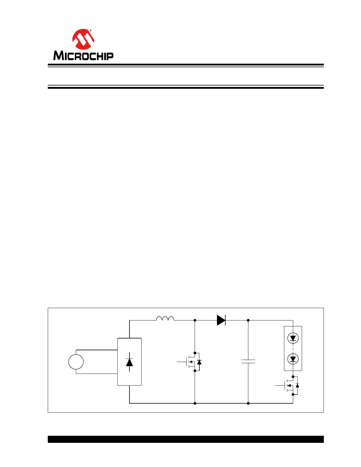
General Description
The HV9805 driver integrated circuit (IC) is targeted at
general LED lighting products, such as LED lamps and
LED lighting fixtures with a maximum power rating of
about 25W at 120V
AC
and about 50W at 230V
AC
.
A two-stage topology provides true constant current
drive for the LED load while drawing mains power with
high power factor. The first stage, a boundary
conduction mode boost converter, transfers power
from the AC line to a second stage with high power
factor and high efficiency. The second stage, a linear
regulator arranged for operation with low overhead
voltage, transfers power from the first stage to the LED
load with true constant current and protects the LED
load from overvoltage that may pass from mains to the
output of the first stage.
The IC is particularly geared to drive a high voltage
LED load. An LED load arranged as a high-voltage load
is capable of offering cost advantages in terms of heat
management and optics.
The boost converter employs a cascode switch for
high-speed switching and convenient generation of the
V
DD
supply. The control device of the cascode switch is
an integral part of the HV9805 and is rated at 700 mA
peak. Current for powering the V
DD
supply is derived
by way of an internal connection to the cascode switch.
Applications with low output voltage can be
accommodated using the SEPIC topology.
Network Topology Diagram
AC
Off-Line LED Driver with True DC Output Current
HV9805
DS20005374A-page 2
2015 Microchip Technology Inc.
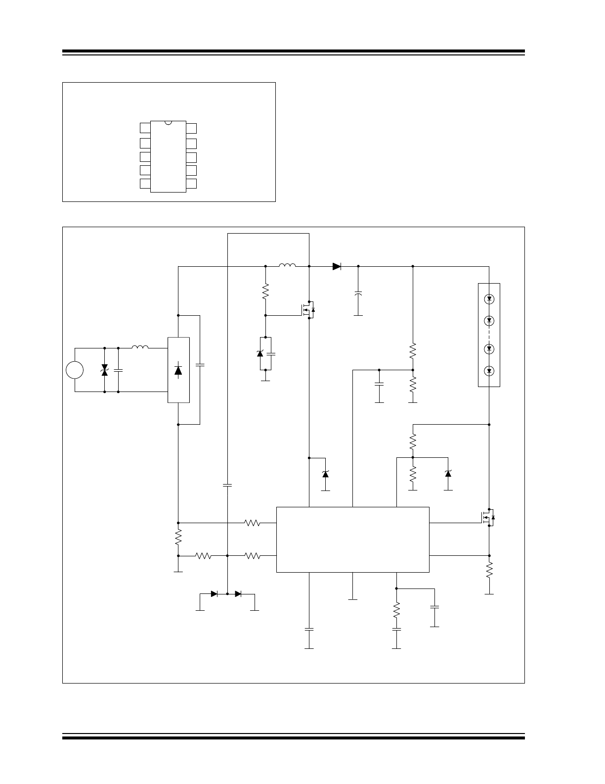
Package Types
Typical Application Circuit
HV9805
MSOP
CSH
CSL
HVS
GND
BVS
1
2
3
4
10
9
8
7 CRG
DRV
V
DD
6 CRS
HVR 5
AC
C
BUS
C
BST
C
REC
C
HVX
C
HVY
C
VAL
C
VDD
D
BST
DN
VAL
BVS
8
CRG
7
CRS
6
CSH
3
CSL
2
DRV
10
GND
9
HVR
5
HVS
4
V
DD
HV9805
L
BST
LED
M
BST
M
CRX
R
LBS
R
BVB
R
BVT
R
CRS
R
CSH
R
CSL
R
HVB
R
HVT
R
BST
R
HVX
R
VAL
Z
DRV
Z
BST
Z
HVS
C
BVS
1
R
CSL
= R
CSA
R
CSH
= R
CSA
+ R
VAL
R
CSA
and R
VAL
: See
Block Diagram
and
Section 3.2
.
2015 Microchip Technology Inc.
DS20005374A-page 3
HV9805
Block Diagram
AC
DRV
BVS
CRG
CRS
CSL
CSH
GND
V
DD
HVR
HVS
R
LBS
C
REC
R
VAL
R
VAL
R
CSA
R
CSA
L
BST
R
BST
Z
BST
C
BST
Z
DRV
C
VAL
D
BST
R
BVT
R
BVB
LED
R
CRS
R
HVB
R
HVT
C
BUS
M
CRX
C
HVX
R
HVX
C
HVY
C
VDD
M
BST
HV9805
Z
HVS
OTP
Inductor
Current
Sense
Linear
V
DD
Regulator
Valley
Detector
Line
Current
Waveform
Regulator
Headroom
Voltage
Regulator
DRV FET
Gate
Logic
Switching
V
DD
Regulator
V
DD
FETs
LED
Current
Sense
LED
Current
Regulator
VDDLO
BVSUV
BVSOV
HVSOK
Comparators
Regulator
Logic
Headroom
Voltage
Sense
C
BVS
OCP
V
BUS
I
LED
V
HEA
I
BST
I
BST
M
1
M
2
DRV
FET

HV9805
DS20005374A-page 4
2015 Microchip Technology Inc.
NOTES:
2015 Microchip Technology Inc.
DS20005374A-page 5
HV9805
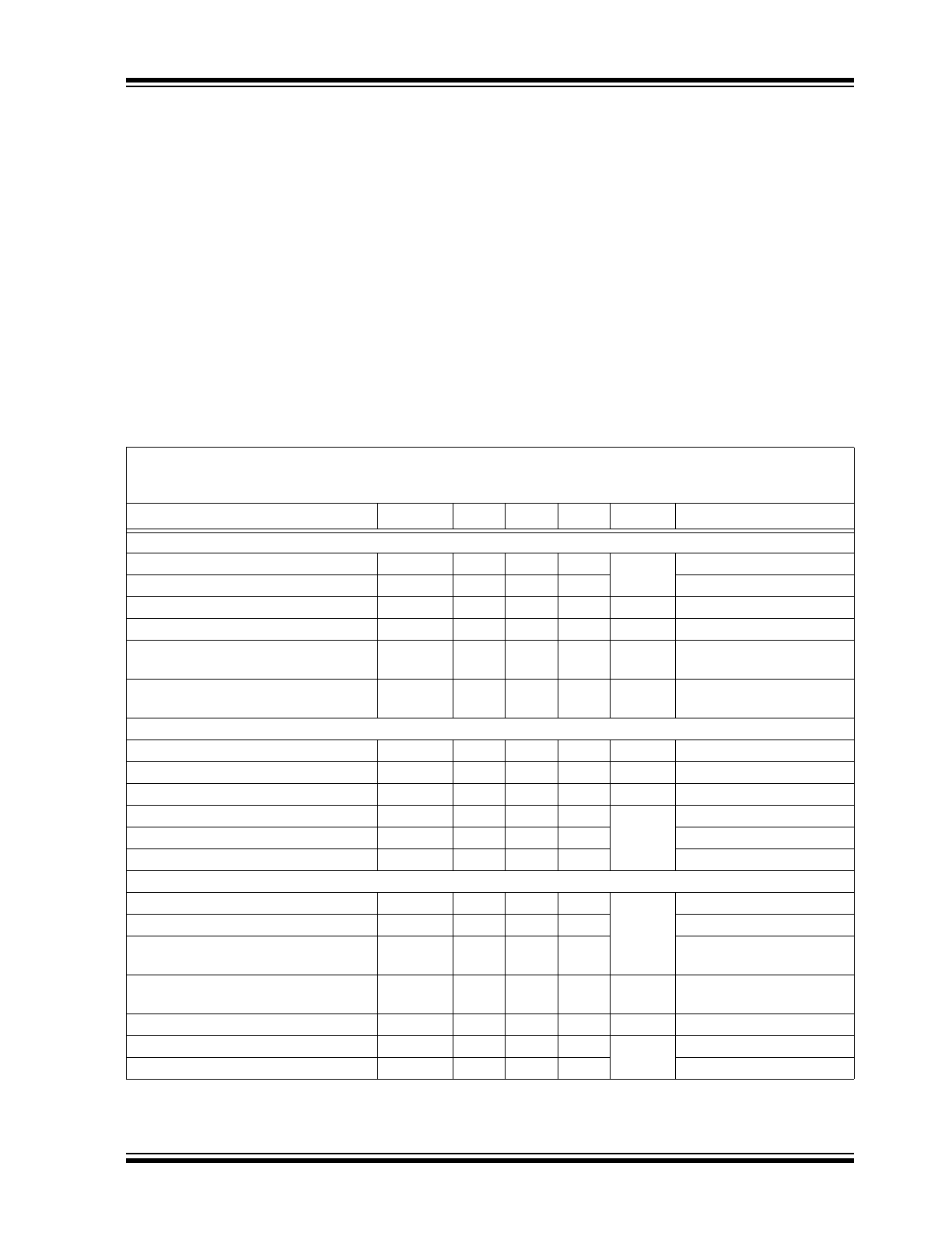
1.0
ELECTRICAL
CHARACTERISTICS
Absolute Maximum Ratings †
V
DD
. . . . . . . . . . . . . . . . . . . . . . . . . . . . . . . . . . . . . . . . . . . . . . . . . . . . . . . . . . . . . . . . . . . . . . . . . . . . . . . -0.5V to +12V
V
DRV
. . . . . . . . . . . . . . . . . . . . . . . . . . . . . . . . . . . . . . . . . . . . . . . . . . . . . . . . . . . . . . . . . . . . . . . . . . . . . . -0.5V to +20V
V
CSL
, V
CSH
, V
BVS
, V
CRS
, V
CRG
, V
HVS
, V
HVR
. . . . . . . . . . . . . . . . . . . . . . . . . . . . . . . . . . . . . . . . . . . . . . -0.5V to +5.5V
Junction Temperature Range . . . . . . . . . . . . . . . . . . . . . . . . . . . . . . . . . . . . . . . . . . . . . . . . . . . . . . . . .-40°C to +125°C
Storage Temperature Range. . . . . . . . . . . . . . . . . . . . . . . . . . . . . . . . . . . . . . . . . . . . . . . . . . . . . . . . . .-65°C to +150°C
Power Dissipation at 25°C . . . . . . . . . . . . . . . . . . . . . . . . . . . . . . . . . . . . . . . . . . . . . . . . . . . . . . . . . . . . . . . . . 625 mW
ESD protection on all pins (HBM) . . . . . . . . . . . . . . . . . . . . . . . . . . . . . . . . . . . . . . . . . . . . . . . . . . . . . . . . . . . . . . . 2 kV
ESD protection on all pins (MM) . . . . . . . . . . . . . . . . . . . . . . . . . . . . . . . . . . . . . . . . . . . . . . . . . . . . . . . . . . . . . . . .150V
† Notice:
Stresses above those listed under “Maximum Ratings” may cause permanent damage to the device. This is
a stress rating only and functional operation of the device at those or any other conditions above those indicated in the
operational sections of this specification is not intended. Exposure to maximum rating conditions for extended periods
may affect device reliability.
DC AND AC CHARACTERISTICS
Electrical Specifications:
Unless otherwise specified, all specifications apply at V
DD
= 8.2V, T
A
= T
J
= +25°C,
f
SWI
= 100 kHz.
Boldface specifications
apply over the ambient temperature (T
A
=
T
J
) range of -40°C to +125°C.
Parameter
Sym.
Min.
Typ.
Max.
Unit
Conditions
V
DD
Supply (V
DD
)
Enable Threshold Voltage
V
ENA
7.2
7.5
7.8
V
V
DD
rising
Disable Threshold Voltage
V
DIS
6.4
6.7
7.1
V
DD
falling
Linear Regulator Resistance
R
REG
0.42
—
1.2
k
V
DD
Voltage
V
DD
7.9
8.2
8.6
V
Switching Regulator Control Gain
K
VDD
= (
T
ON,VDDFET
)/(
V
DD
)
K
VDD
—
3
—
µs/V
V
DD
= 8.0V (
Note 2
)
Supply Current, RUN State,
Measured at DRV Pin
I
DD
1
2.5
5
mA
First Stage, Boost Regulator (DRV)
Control FET On-Resistance
R
DRV
—
1
—
Note 2
Overcurrent Comparator Threshold
I
OCP
0.75
—
2.75
A
Overcurrent Comparator Blanking Time
T
BLK
—
330
—
ns
Note 2
Nominal On-Time
T
ONN
—
2.7
—
µs
V
HVR
= 1.2V (
Note 2
)
Maximum On-Time
T
ONH
8
—
13
Maximum Off-Time
T
OFH
80
—
110
Headroom Voltage Regulator (HVS, HVR)
Regulator Reference Voltage
V
REF,HVR
1.17
1.25
1.32
V
Run Comparator Threshold
V
RUN
—
1.25
—
Note 2
Regulator Output Voltage,
Maximum Level
V
HVR
—
5.0
5.5
Regulator Control Gain
K
HVR
= (
T
ON, DRVFET
)/(
V
HVR
)
K
HVR
—
2.2
—
µs/V
V
HVR
= 1.0V (
Note 2
)
Control Amplifier Transconductance
G
HVR
55
75
95
µA/V
Control Amplifier Sink Current
I
SNK,HVR
50
—
80
µA
V
HVR
= 2.5V, V
HVS
= 2.25V
Control Amplifier Source Current
I
SRC,HVR
50
—
80
V
HVR
= 2.5V, V
HVS
= 0.25V
Note 1:
Specification is obtained by characterization and is not 100% tested.
2:
Specification is for design guidance only.
HV9805
DS20005374A-page 6
2015 Microchip Technology Inc.
Current Sense Amplifier (CSL, CSH)
Sense Amplifier Transresistance
R
CSA
—
10
—
mV/µA
Note 1
Sense Amplifier Input Current Range
I
CSA
-100
—
100
µA
Note 2
Valley Detection Propagation Delay
TP
VAL
50
120
200
ns
Overdrive Current
(I
CSH
– I
CSL
) = -5 µA
Bus Voltage Comparators (BVS)
Undervoltage Upper Threshold
V
UVU
0.45
0.5
0.55
V
V
BVS
rising
Undervoltage Lower Threshold
V
UVL
0.36
0.4
0.46
V
BVS
falling
Overvoltage Upper Threshold
V
OVU
1.19
1.25
1.31
V
BVS
rising
Overvoltage Lower Threshold
V
OVL
1.11
1.15
1.2
V
BVS
falling
Second Stage, Constant Current Regulator (CRS, CRG)
Regulator Reference Voltage
V
REF,CCR
0.96
1.00
1.04
V
Soft-Start Reference Level
V
SSR
—
20
—
%V
REF
Note 2
Gate Output Voltage, Maximum Level
V
CRG
4.5
—
5.5
V
Gate Output Current, Sinking
I
SNK,CCR
1
2
—
mA
V
CRG
= 4.0V
Gate Output Current, Sourcing
I
SRC,CCR
1
1.5
—
V
CRG
= 0V
Overtemperature Protection
Disable Threshold
T
DIS
—
145
—
°C
Note 1
Enable Threshold
T
ENA
—
130
—
°C
Note 1
TEMPERATURE SPECIFICATIONS
Electrical Specifications:
Unless otherwise specified, all voltages are referenced to the GND pin, T
A
= T
J
= +25°C.
Boldface specifications
apply over the full operating ambient temperature (T
A
) range of -40°C to +125°C.
Parameters
Sym.
Min.
Typ.
Max.
Units
Conditions
Temperature Ranges
Operating Ambient Temperature
Range
T
A
-40
—
+125
°C
Storage Temperature Range
T
A
-65
—
+150
°C
Maximum Junction Temperature
T
J
-40
—
+150
°C
Package Thermal Resistances
Thermal Resistance, 10L-MSOP
JA
—
202
—
°C/W
DC AND AC CHARACTERISTICS (CONTINUED)
Electrical Specifications:
Unless otherwise specified, all specifications apply at V
DD
= 8.2V, T
A
= T
J
= +25°C,
f
SWI
= 100 kHz.
Boldface specifications
apply over the ambient temperature (T
A
=
T
J
) range of -40°C to +125°C.
Parameter
Sym.
Min.
Typ.
Max.
Unit
Conditions
Note 1:
Specification is obtained by characterization and is not 100% tested.
2:
Specification is for design guidance only.
2015 Microchip Technology Inc.
DS20005374A-page 7
HV9805
2.0
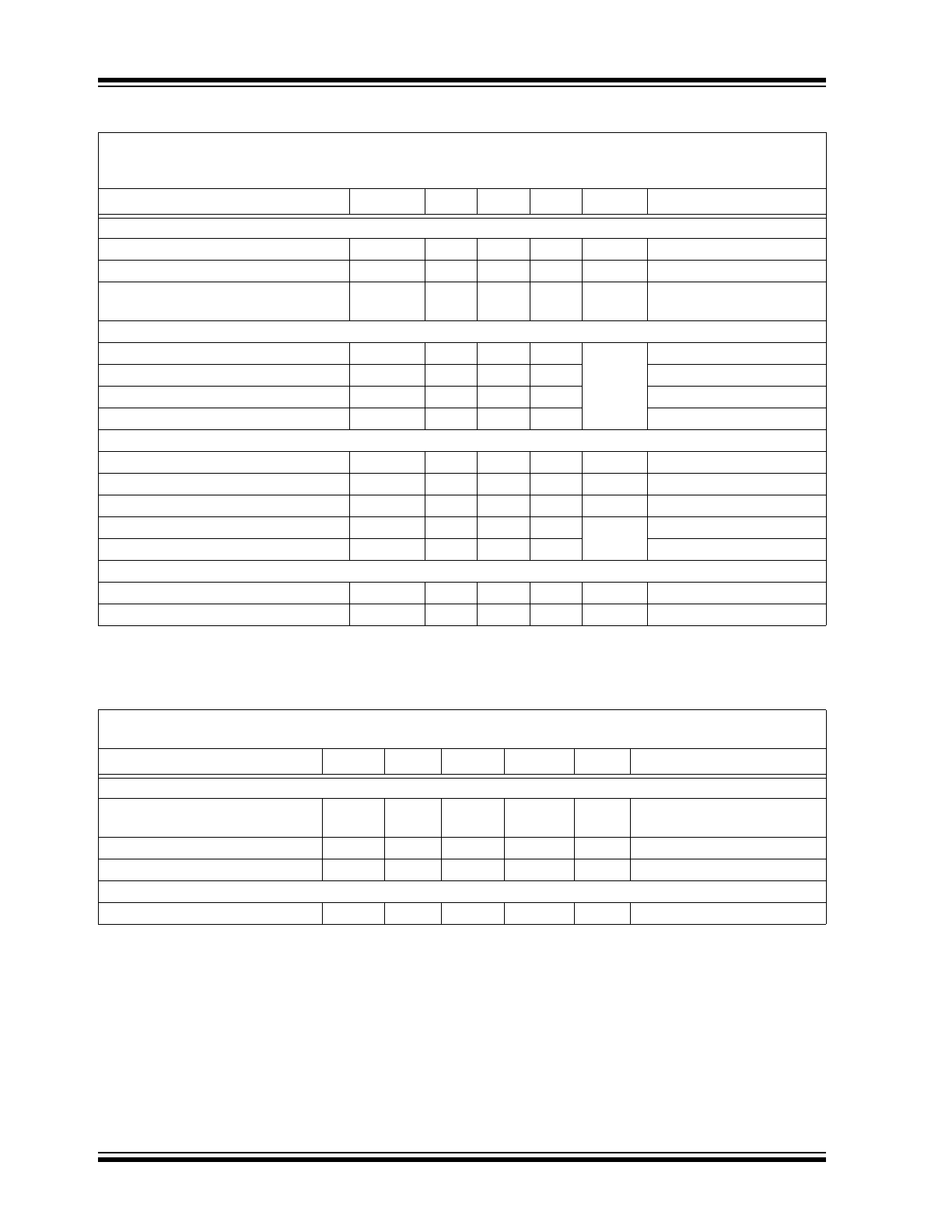
TYPICAL PERFORMANCE CURVES
Note:
Unless otherwise indicated, V
DD
= 8.2V, T
A
= +25°C, f
SWI
= 100 kHz.
FIGURE 2-1:
V
DD
Supply Enable Voltage
vs. Temperature.
FIGURE 2-2:
V
DD
Supply Disable Voltage
vs. Temperature.
FIGURE 2-3:
V
DD
Supply Linear
Regulator Resistance vs. Temperature.
FIGURE 2-4:
V
DD
Supply Regulation
Voltage vs Temperature.
FIGURE 2-5:
V
DD
Supply Current Draw
vs. Temperature.
FIGURE 2-6:
Overcurrent Threshold vs.
Temperature.
Note:
The graphs and tables provided following this note are a statistical summary based on a limited number of
samples and are provided for informational purposes only. The performance characteristics listed herein
are not tested or guaranteed. In some graphs or tables, the data presented may be outside the specified
operating range (e.g., outside specified power supply range) and therefore outside the warranted range.
0
1
2
3
4
5
6
7
8
9
10
-50
-25
0
25
50
75
100
125
150
V
DD
Enable V
o
ltage (V)
Temperature (°C)
V
ENA
0
1
2
3
4
5
6
7
8
9
10
-50
-25
0
25
50
75
100
125
150
V
DD
Disable V
o
ltage (V)
Temperature (°C)
V
DIS
0.0
0.5
1.0
1.5
2.0
-50
-25
0
25
50
75
100
125
150
V
DD
6XSSO\
/LQHDU5HJXODWRUNȍ
Temperature (°C)
R
REG
0
1
2
3
4
5
6
7
8
9
10
-50
-25
0 25
50
75
100
125
150
V
DD
V
o
ltage (V)
Temperature (°C)
V
DD
0
1
2
3
4
5
-50
-25
0 25
50
75
100
125
150
V
DD
Supply
Current
(mA)
Temperature (°C)
I
DD
0
1
2
3
4
-50
-25
0
25
50
75
100
125
150
Overcurrent Threshold (A)
Temperature (°C)
I
OCP
HV9805
DS20005374A-page 8
2015 Microchip Technology Inc.
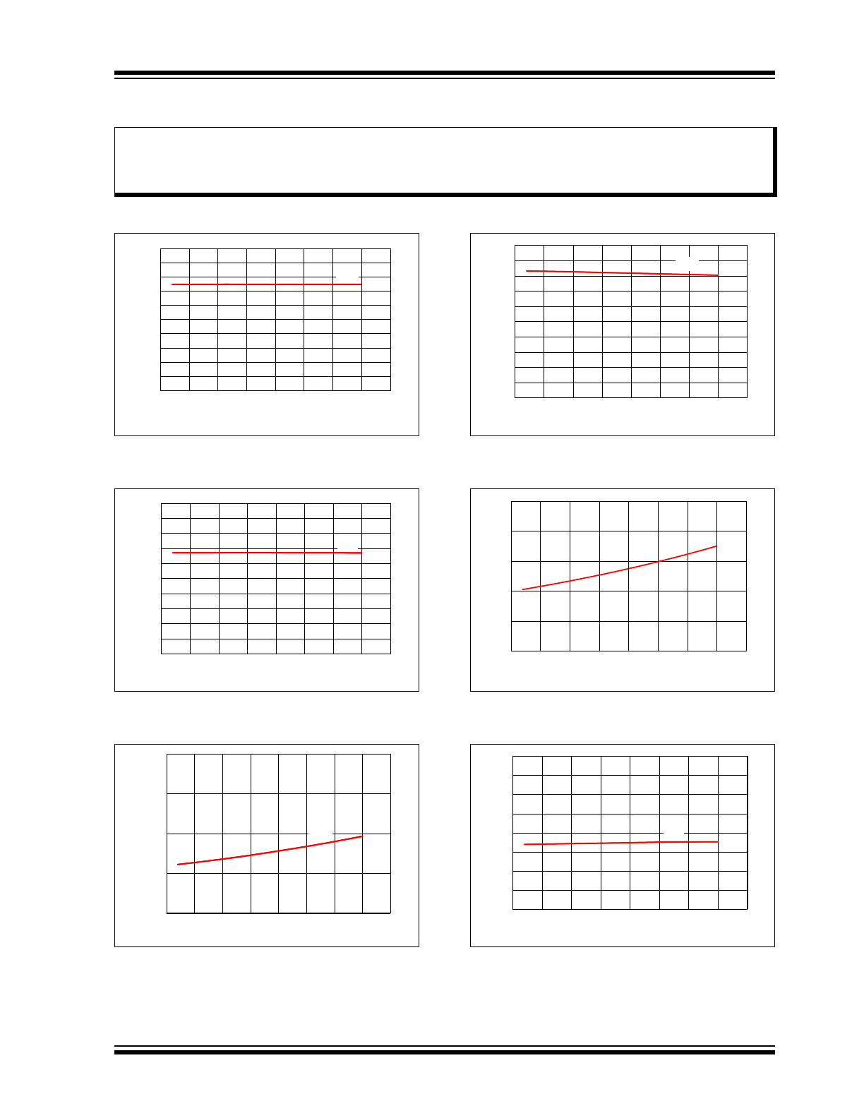
Note:
Unless otherwise indicated, V
DD
= 8.2V, T
A
= +25°C, f
SWI
= 100 kHz.
FIGURE 2-7:
Maximum On-Time vs.
Temperature.
FIGURE 2-8:
Maximum Off-Time vs.
Temperature.
FIGURE 2-9:
Headroom Voltage
Regulator Reference Voltage vs. Temperature
(RUN State).
FIGURE 2-10:
HVR Transconductance vs.
Temperature.
FIGURE 2-11:
HVR Maximum Source
Current vs. Temperature.
FIGURE 2-12:
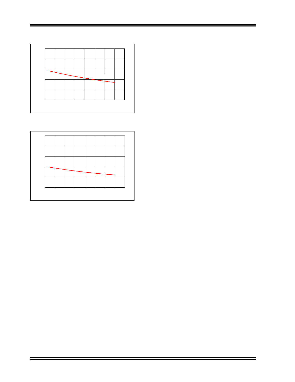
HVR Maximum Sink Current
vs. Temperature.
0
5
10
15
20
-50
-25
0
25
50
75
100
125
150
Maximum On-T
ime (µs)
Temperature (°C)
T
ONH
0
25
50
75
100
-50
-25
0
25
50
75
100
125
150
Maximum Off-T
ime (µs)
Temperature (°C)
T
OFH
1.20
1.25
1.30
-50
-25
0
25
50
75
100
125
150
HVR Reference V
o
ltage (V)
Temperature (°C)
V
REF,HVR
0
25
50
75
100
-50
-25
0
25
50
75
100
125
150
HVR T
ransconductance
(µA/V)
Temperature (°C)
G
HVR
0
25
50
75
100
-50
-25
0
25
50
75
100
125
150
HVR Source Current (µA)
Temperature (°C)
I
SRC,HVR
0
25
50
75
100
-50
-25
0
25
50
75
100
125
150
HVR Sink Current (µA)
Temperature (°C)
I
SNK,HVR
2015 Microchip Technology Inc.
DS20005374A-page 9
HV9805
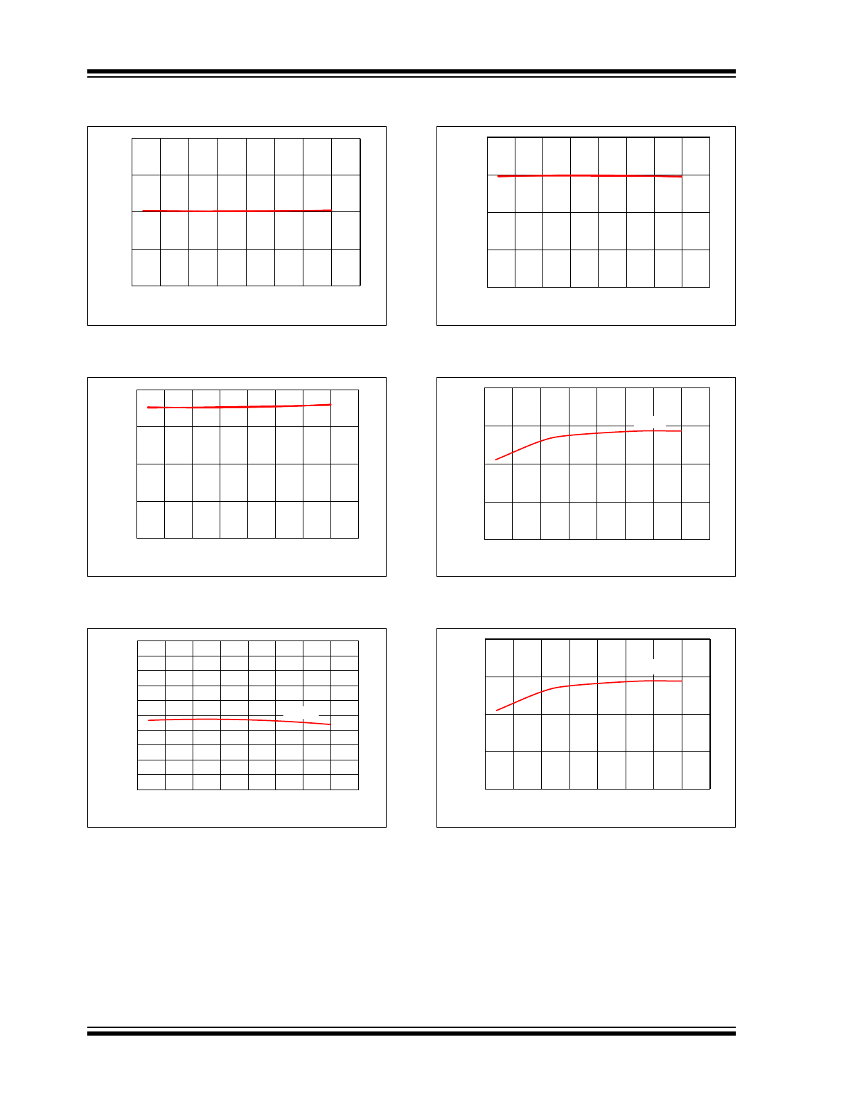
Note:
Unless otherwise indicated, V
DD
= 8.2V, T
A
= +25°C, f
SWI
= 100 kHz.
FIGURE 2-13:
Valley Detector Propagation
Delay vs. Temperature.
FIGURE 2-14:
Undervoltage Upper
Threshold Voltage vs. Temperature.
FIGURE 2-15:
Undervoltage Lower
Threshold Voltage vs. Temperature.
FIGURE 2-16:
Overvoltage Upper
Threshold Voltage vs. Temperature.
FIGURE 2-17:
Overvoltage Lower
Threshold Voltage vs. Temperature.
FIGURE 2-18:
Constant Current Regulator
Reference Voltage vs. Temperature (RUN State).
0
50
100
150
200
-50
-25
0
25
50
75
100
125
150
V
a
lley
Detection
Delay
(ns)
Temperature ( C)
TP
VAL
0.0
0.5
1.0
-50
-25
0
25
50
75
100
125
150
Undervoltage
Upper Threshold
(V)
Temperature (°C)
V
UVU
0.0
0.5
1.0
-50
-25
0
25
50
75
100
125
150
Undervoltage
Low
er Threshold
(V)
Temperature (°C)
V
UVL
0.0
0.5
1.0
1.5
2.0
-50
-25
0
25
50
75
100
125
150
Overvoltage
Upper Threshold
(V)
Temperature (°C)
V
OVU
0.0
0.5
1.0
1.5
2.0
-50
-25
0
25
50
75
100
125
150
Overvoltage
Low
er Threshold
(V)
Temperature (°C)
V
OVL
0.90
0.92
0.94
0.96
0.98
1.00
1.02
1.04
1.06
1.08
1.10
-50
-25
0
25
50
75
100
125
150
CCR Reference V
o
ltage (V)
Temperature ( C)
V
REF,CCR
HV9805
DS20005374A-page 10
2015 Microchip Technology Inc.
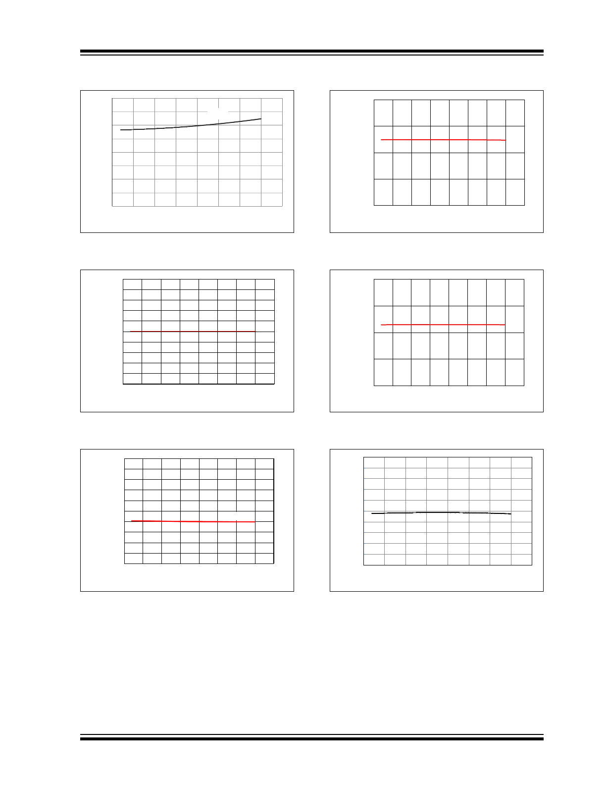
Note:
Unless otherwise indicated, V
DD
= 8.2V, T
A
= +25°C, f
SWI
= 100 kHz.
FIGURE 2-19:
CRG Gate Sink Current vs.
Temperature.
FIGURE 2-20:
CRG Gate Source Current
vs. Temperature.
0
1
2
3
4
5
-50
-25
0
25
50
75
100
125
150
CRG Sink Current (mA)
Temperature (°C)
I
SNK,CCR
0
1
2
3
4
5
-50
-25
0
25
50
75
100
125
150
CRG Source
Current (mA)
Temperature (°C)
I
SRC,CCR