
2017 Microchip Technology Inc.
DS20005642A-page 1
HV9803B
Features
• Fast Average Current Control
• Correction for Propagation Delay and Offset
Voltage
• Fixed Off-time Switching Mode
• Linear Dimming Input
• PWM Dimming Input
• Output Short-circuit Protection with
Programmable Skip Mode
• Input Undervoltage Shutdown
Applications
• Backlighting of LCD Panels
• General Lighting
General Description
The HV9803B is an open-loop, Average-mode current
control LED driver IC operating in a constant Off-time
mode. The IC features ±2% current accuracy and tight
line and load regulation of the LED current without any
need for loop compensation or high-side current
sensing. Its auto-zero circuit cancels the effect of both
the input offset voltage and the propagation delay in the
current sense comparator.
The HV9803B can be powered from a 7V to 16V
supply. The IC features fast PWM dimming response.
The linear dimming input LD can accept a reference
voltage from 0V to 3V.
The IC is equipped with a current limit comparator for
Hiccup-mode output short-circuit protection. It also
features a programmable input undervoltage
shutdown.
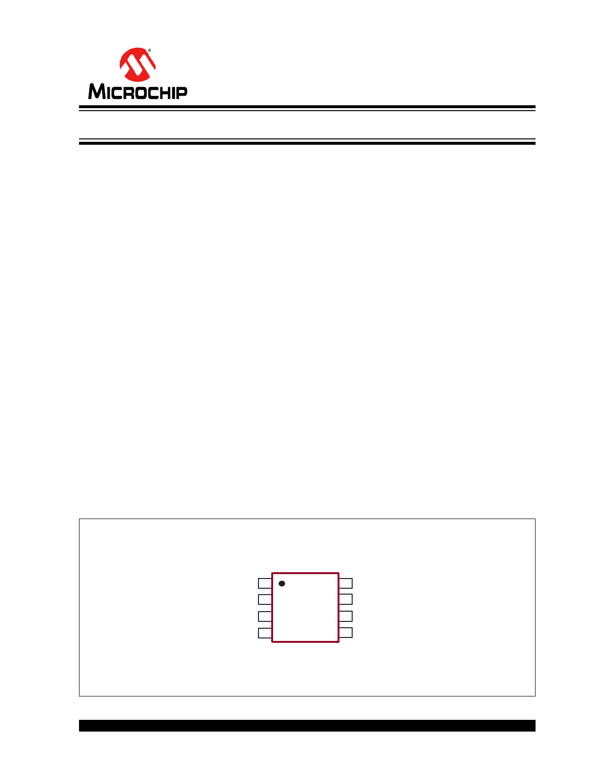
Package Type
See
Table 2-1
for pin information.
1
2
3
4
8
7
6
5
CS
VDD
GND
GATE
LD
UVLO
PWMD
RT
8-lead SOIC
(Top view)
LED Driver IC with Average-Mode Constant Current Control
VDD
LD
CS
GND
TOFF
Timer
R Q
S Q
Q S
R
Average-Mode
Control Logic
Auto-REF
xA
V(LD)
POR
Current
Mirror
V
LIM
i
i
+
-
-
+
+
-
+
-
UVLO
GATE
PWMD
RT
SKIP
Reset
OUT
IN
SKIP
UVLO1
V
LD
UVLO2
Reset
I
RT(LIM)
250mV
HV9803B
L/E
Blanking
10mV
HV9803B
DS20005642A-page 2
2017 Microchip Technology Inc.
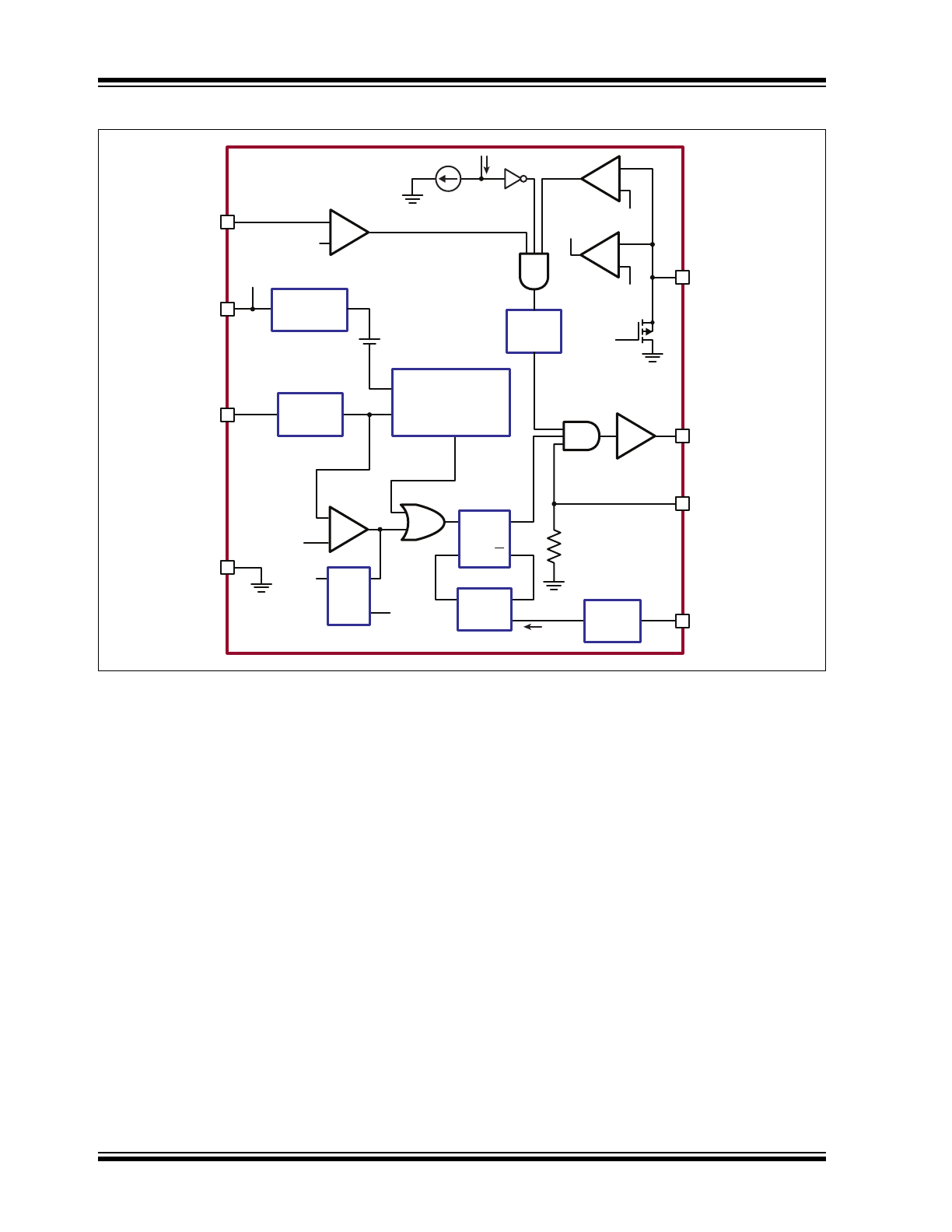
Functional Block Diagram
2017 Microchip Technology Inc.
DS20005642A-page 3
HV9803B
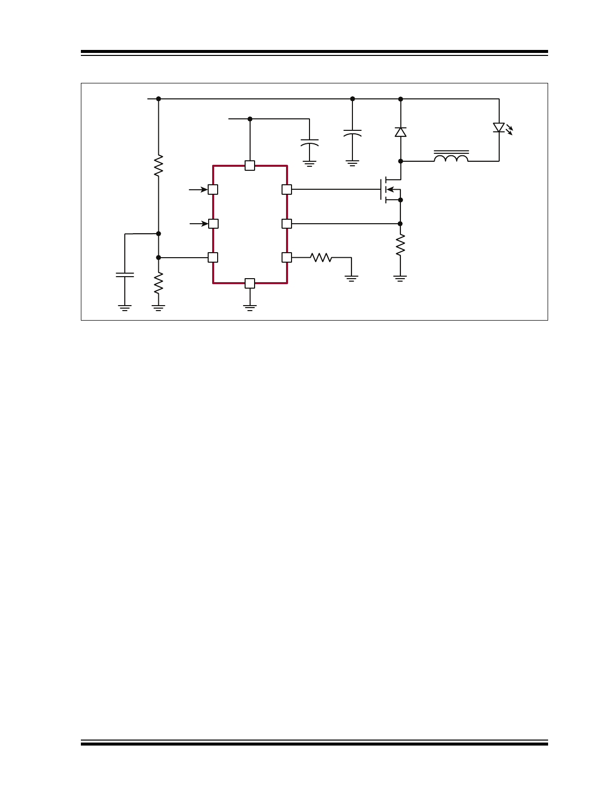
Typical Application Circuit
+V
IN
7.0~16V
R
CS
R
T
REF
DIM
R
2
R
1
C
SKIP
HV9803B
VDD
PWMD
LD
UVLO
GATE
CS
RT
GND
C
DD
C
IN
D
1
L
1
Q
1
HV9803B
DS20005642A-page 4
2017 Microchip Technology Inc.
1.0
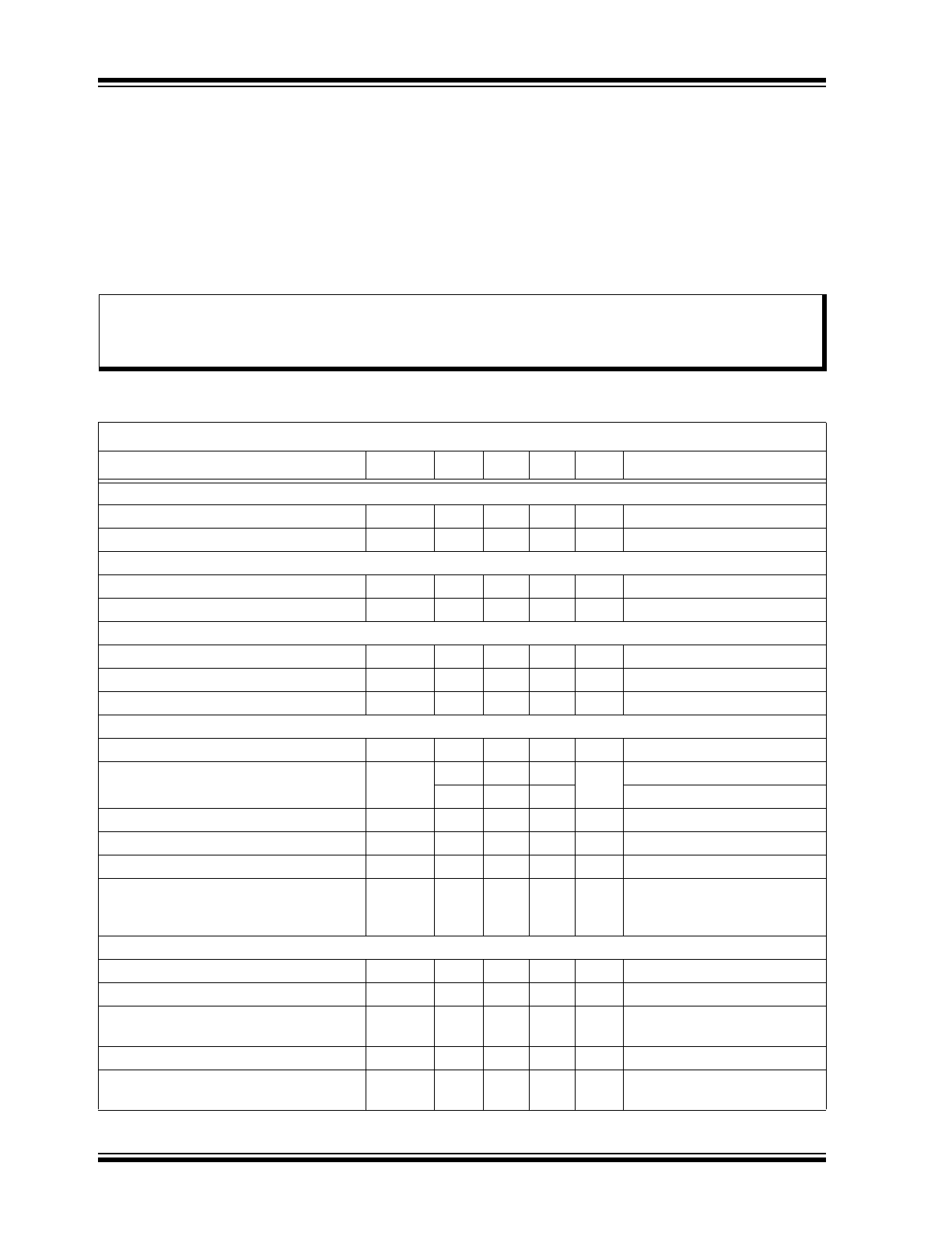
ELECTRICAL CHARACTERISTICS
Absolute Maximum Ratings†
V
DD
, Gate, CS ...........................................................................................................................................–0.3V to +17V
LD, RT, PWMD, UVLO ............................................................................................................................... –0.3V to +6V
Operating Junction Temperature Range, T
J
........................................................................................ –40°C to +125°C
Storage Temperature Range, T
S
......................................................................................................... –65°C to +150°C
Power Dissipation (at 25 °C):
8-lead SOIC
............................................................................................................................................ 650 mW
† Notice: Stresses above those listed under “Absolute Maximum Ratings” may cause permanent damage to the
device. This is a stress rating only, and functional operation of the device at those or any other conditions above those
indicated in the operational sections of this specification is not intended. Exposure to maximum rating conditions for
extended periods may affect device reliability.
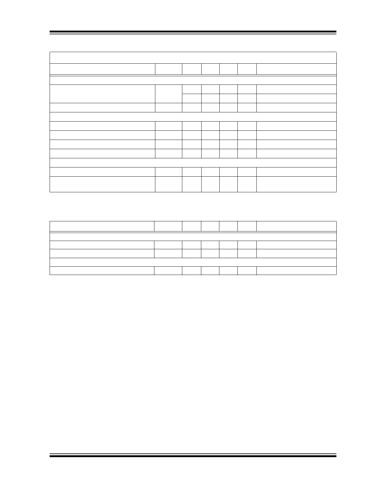
ELECTRICAL CHARACTERISTICS
Electrical Specifications: Unless otherwise noted, T
A
= T
J
=
+25°C, V
DD
= 12V and PWMD = 5V.
Parameter
Sym.
Min.
Typ.
Max.
Unit
Conditions
INPUT
Input DC Supply Voltage Range
V
DD
—
—
16
V
DC input voltage (
Note 1
)
Quiescent V
DD
Supply Current
I
DD
—
1.5
2.5
mA
V
CS
= 0V (
Note 1
)
V
DD
UNDERVOLTAGE LOCKOUT
V
DD
Undervoltage Lockout Threshold
V
DD(UV)
6.45
6.7
6.95
V
V
DD
rising (
Note 1
)
V
DD
Undervoltage Lockout Hysteresis
∆V
DD(UV)
—
500
—
mV
V
DD
falling
PWM DIMMING
PWMD Input Low Voltage
V
EN(LO)
—
—
1
V
Note 1
PWMD Input High Voltage
V
EN(HI)
2.6
—
—
V
Note 1
Internal Pull-down Resistance at PWMD
R
EN
50
100
150
kΩ
CURRENT SENSE COMPARATOR
External Reference Voltage
V
LD
0
—
3
V
CS Reference Voltage
V
CS
284
—
296
mV
V
LD
= 0.6V (
Note 1
)
866
—
902
V
LD
= 1.8V (
Note 1
)
LD to CS Voltage Ratio
A
V(LD)
—
0.495
—
—
Current Sense Blanking Interval
T
BLANK
150
—
280
ns
Note 1
Minimum On-time
T
ON(MIN)
—
—
760
ns
V
CS
= 0.5 V
LD
+ 30 mV
Maximum Steady State Duty Cycle
D
MAX
85
—
—
%
Reduction in output LED
current may occur beyond this
duty cycle. (
Note 1
)
SHORT-CIRCUIT PROTECTION
Internal Current Reference
V
LIM
1.57
—
1.93
V
Current Limit Delay CS-to-Gate
T
DELAY
—
—
150
ns
V
CS
= V
LIM
+ 30 mV
UVLO Skip Timer Reset Switch
Resistance
R
UVLO(R)
—
—
500
Ω
UVLO Skip Timer Reset Voltage
V
UVLO(R)
200
—
300
mV
Minimum On-time
(Short Circuit)
T
ON(MIN)
—
—
430
ns
V
CS
= V
LIM
+ 30 mV
Note 1: Applies over the full operating temperature range of –40°C < T
A
(= T
J
) < +125°C
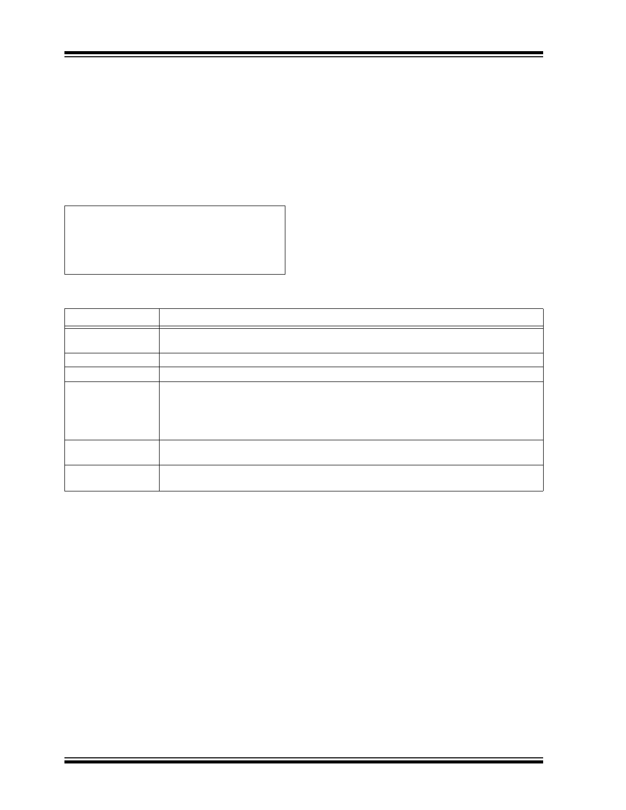
2017 Microchip Technology Inc.
DS20005642A-page 5
HV9803B
T
OFF
TIMER
Off-time
T
OFF
6.7
9
11.3
μs
R
T
= 250 kΩ
0.8
1
1.2
μs
R
T
= 25 kΩ
R
T
Overcurrent Threshold
I
RT(LIM)
—
2.8
—
mA
GATE DRIVER
Gate Sourcing Current
I
SOURCE
0.165
—
—
A
V
GATE
= 0V
Gate Sinking Current
I
SINK
0.165
—
—
A
V
GATE
= V
DD
Gate Output Rise Time
t
RISE
—
30
50
ns
C
GATE
= 500 pF
Gate Output Fall Time
t
FALL
—
30
50
ns
C
GATE
= 500 pF
UVLO
Undervoltage Threshold Voltage
UVLO
1.17
—
1.29
V
V
UVLO
rising (
Note 1
)
Undervoltage Threshold Voltage
Hysteresis
∆UVLO
—
150
—
mV
V
UVLO
falling
TEMPERATURE SPECIFICATIONS
Parameter
Sym.
Min.
Typ.
Max.
Unit
Conditions
TEMPERATURE RANGE
Operating Junction Temperature
T
J
–40
—
+125
°C
Storage Temperature
T
S
–65
—
+150
°C
PACKAGE THERMAL RESISTANCE
8-lead SOIC
JA
—
101
—
°C/W
ELECTRICAL CHARACTERISTICS (CONTINUED)
Electrical Specifications: Unless otherwise noted, T
A
= T
J
=
+25°C, V
DD
= 12V and PWMD = 5V.
Parameter
Sym.
Min.
Typ.
Max.
Unit
Conditions
Note 1: Applies over the full operating temperature range of –40°C < T
A
(= T
J
) < +125°C

HV9803B
DS20005642A-page 6
2017 Microchip Technology Inc.
2.0
PIN DESCRIPTION
The details on the pins of HV9803B are listed on
Table 2-1
. See location of pins in
Package Type
.
TABLE 2-1:
PIN FUNCTION TABLE
Pin Number
Pin Name
Description
1
CS
This pin is the current sense pin used to detect the MOSFET source current by
means of an external sense resistor.
2
VDD
This is the power supply input for the gate output and input of the low-voltage regu-
lator powering the internal logic. It must be bypassed with a low-ESR capacitor to
GND (at least 0.1 μF).
3
GND
Ground return for all internal circuitry. This pin must be electrically connected to the
ground of the power train.
4
GATE
This pin is the output gate driver for an external N-channel power MOSFET.
5
RT
A resistor connected between R
T
and GND programs the gate off-time
6
PWMD
This is the PWM dimming input of the IC. When this pin is pulled to GND, the gate
driver is turned off. When the pin is pulled high, the gate driver operates normally.
7
UVLO
This pin is the undervoltage comparator input. It is also used to form a short-circuit
protection skip delay.
8
LD
This pin is the reference voltage input for programming the LED current.

2017 Microchip Technology Inc.
DS20005642A-page 7
HV9803B
3.0
FUNCTIONAL DESCRIPTION
3.1
General
The peak-current control of a buck converter is an
economical and simple way to regulate its output
current. However, it suffers accuracy and regulation
problems that arise from the peak-to-average current
error due to the current ripple in the output inductor and
the propagation delay in the current sense comparator.
The full inductor current signal is unavailable for direct
sensing at the ground potential in a buck converter
when the control switch is referenced to the same
ground potential. While it is very simple to detect the
peak current in the switch, controlling the average
inductor current is usually implemented by
level-translating the current sense signal from the
positive input supply rail. While this is practical for
relatively low-input voltage, this type of average-current
control may become excessively complex and
expensive in the case of input voltages above 100V.
The HV9803B uses a control scheme that achieves
fast and highly accurate control of average current in
the buck inductor by only sensing the switch current.
No compensation of the current control loop is
required. The inductor current ripple amplitude does
not affect this control scheme significantly. The LED
current is independent of the variation in inductance,
switching frequency and output voltage. Constant
off-time control of the buck converter is used for
stability and to improve the LED current regulation over
a wide range of input voltages. The IC features
excellent PWM dimming response.
3.2
OFF Timer
In the HV9803B, the timing resistor connected at the R
T
pin determines the off-time of the gate driver, and the
resistor must be wired to GND. The equation governing
the off-time of the gate output is derived with
Equation 3-1
.
EQUATION 3-1:
T
OFF
R
T
40pF
=
The R
T
input is protected from short circuit.
Overcurrent condition at R
T
inhibits the IC.
3.3
Current Sense Comparator and
Timer Circuits
The function of the HV9803B’s current sense
comparator is similar to that of a peak-current
controller. However, the gate pulse is not terminated
immediately as the LD threshold is met. The gate
turn-off in the nth cycle is delayed by a time T
2,n
determined by a timer circuit as shown in
Equation 3-2
.
EQUATION 3-2:
T
2 n
1
2
---
T
1 n
T
1 n 1
–
+
=
Where T
1,n
and T
1,n-1
are the times to the LD
threshold in any two consecutive switching cycles.
This iterative control law is needed for damping
sub-harmonic oscillation. Note that the control law is
only valid up to a maximum switching duty cycle,
D
MAX
= 0.85. Exceeding D
MAX
will cause a reduction in
the LED current.
Propagation delay in the current sense comparator is
one of the most significant contributors to the LED
current error. It must be noted that the control scheme
described above does not improve this deficiency of
the peak-current control scheme by itself. Moreover, it
samples the propagation delay during T
1
and replicates
it during T
2
, essentially doubling the error introduced by
this delay. To eliminate this error, the reference voltage
is corrected by an auto-zero circuit. In essence, the
HV9803B samples its CS signal when the current
sense comparator triggers and detects the difference
between the sampled CS level and the reference input
of the current sense comparator. The resulting
difference is subtracted from the reference level to
generate a new reference in the next switching cycle.
3.4
Gate Output
The gate output of the HV9803B is used to drive an
external MOSFET. It is recommended that the gate
charge Q
G
of the external MOSFET be less than 25 nC
for switching frequencies ≤100 kHz and less than
15 nC for switching frequencies >100 kHz.
The resulting LED current is calculated using
Equation 3-3
.
EQUATION 3-3:
I
LED
0.495 V
LD
7mV
–
R
CS
-----------------------------------------------
=
HV9803B
DS20005642A-page 8
2017 Microchip Technology Inc.
3.5
Short-circuit Protection
The HV9803B is equipped with a protection
comparator having a CS threshold V
LIM
. When this
second threshold is triggered, the gate output shuts off
for the duration of a restart delay, determined by the RC
constant at UVLO. The capacitor C
SKIP
is discharged
below 200 mV. A restart delay due to charging C
SKIP
to
the UVLO start threshold is calculated as shown in
Equation 3-4
.
EQUATION 3-4:
T
SKIP
k R
1
C
SKIP
In
k V
IN
0.30V
–
k V
IN
1.17V
–
--------------------------------------
=
Where:
k
R
2
R
1
R
2
+
------------------
=
3.6
Undervoltage Shutdown
Undervoltage comparator input is provided to disable
the IC when the UVLO input is below a threshold.
Hysteresis is provided to avoid oscillation.
3.7
Failure Modes and Effects
Analysis (FMEA)
The HV9803B is designed to withstand short circuit
between its adjacent pins without damage.
Table 3-1
describes the effect of such incidental short-circuit
conditions.
TABLE 3-1:
FAILURE MODES AND ANALYSIS
Short-circuit Mode
Effect
CS to V
DD
The IC triggers the short-circuit protection and operates in the Auto-restart mode continu-
ously.
V
DD
to GND
Short circuit across the 12V should cause the external bias supply overcurrent protection.
GND to GATE
Should cause the external bias supply overcurrent protection. The power MOSFET Q1 is off.
R
T
to PWMD
Case 1–PWMD = Lo: The R
T
pin sources its maximum current.
GATE = 0V and Q1 is off.
Case 2–PWMD = Hi: The R
T
pin is pulled up, shutting off the timer.
GATE is off.
PWMD to UVLO
This will overdrive the undervoltage threshold. However, since the V
IN
UV condition is harm-
less to the IC, there is no effect.
UVLO to LD
LD overdrives the UVLO. If LD is lower than the UVLO threshold, the IC shuts off. No effect
otherwise.
2017 Microchip Technology Inc.
DS20005642A-page 9
HV9803B
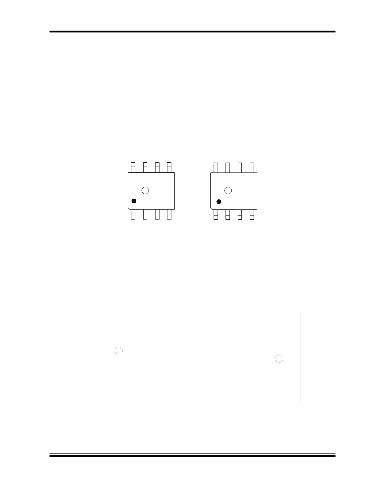
4.0
PACKAGING INFORMATION
4.1
Package Marking Information
Legend: XX...X
Product Code or Customer-specific information
Y
Year code (last digit of calendar year)
YY
Year code (last 2 digits of calendar year)
WW
Week code (week of January 1 is week ‘01’)
NNN
Alphanumeric traceability code
Pb-free JEDEC
®
designator for Matte Tin (Sn)
*
This package is Pb-free. The Pb-free JEDEC designator ( )
can be found on the outer packaging for this package.
Note:
In the event the full Microchip part number cannot be marked on one line, it will
be carried over to the next line, thus limiting the number of available
characters for product code or customer-specific information. Package may or
not include the corporate logo.
3
e
3
e
8-lead SOIC
Example
NNN
XXXXXXXX
YYWW
e3
491
HV9803B
1723
LG
XX
e3
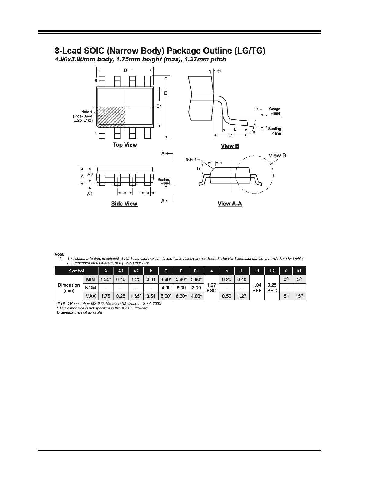
Note: For the most current package drawings, see the Microchip Packaging Specification at www.microchip.com/packaging.
HV9803B
DS20005642A-page 10
2017 Microchip Technology Inc.