
2017 Microchip Technology Inc.
DS20005692A-page 1
HV9801A
Features
• Four-level Switch Dimming
• Highly Accurate Current Regulator
• Output Overcurrent or Short-circuit Protection
• IC Overtemperature Protection
Applications
• Switch-dimmable LED Bulbs and Fixtures
General Description
The HV9801A LED driver is ideally suited for
switch-dimmable applications using LED bulbs and
fixtures.
Through switch dimming, the lamp can be adjusted to
four discrete brightness levels by rapid cycling of the
light switch. The brightness levels are traversed in an
up-and-down manner. Brightness resumes at the
highest level when power is removed for more than a
second.
The device can be powered directly from rectified AC
through an internal V
DD
regulator rated at 450V.
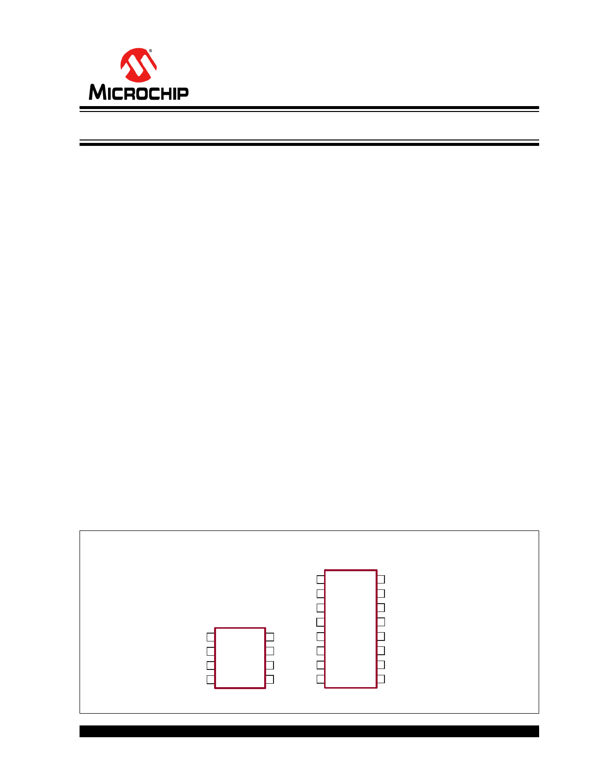
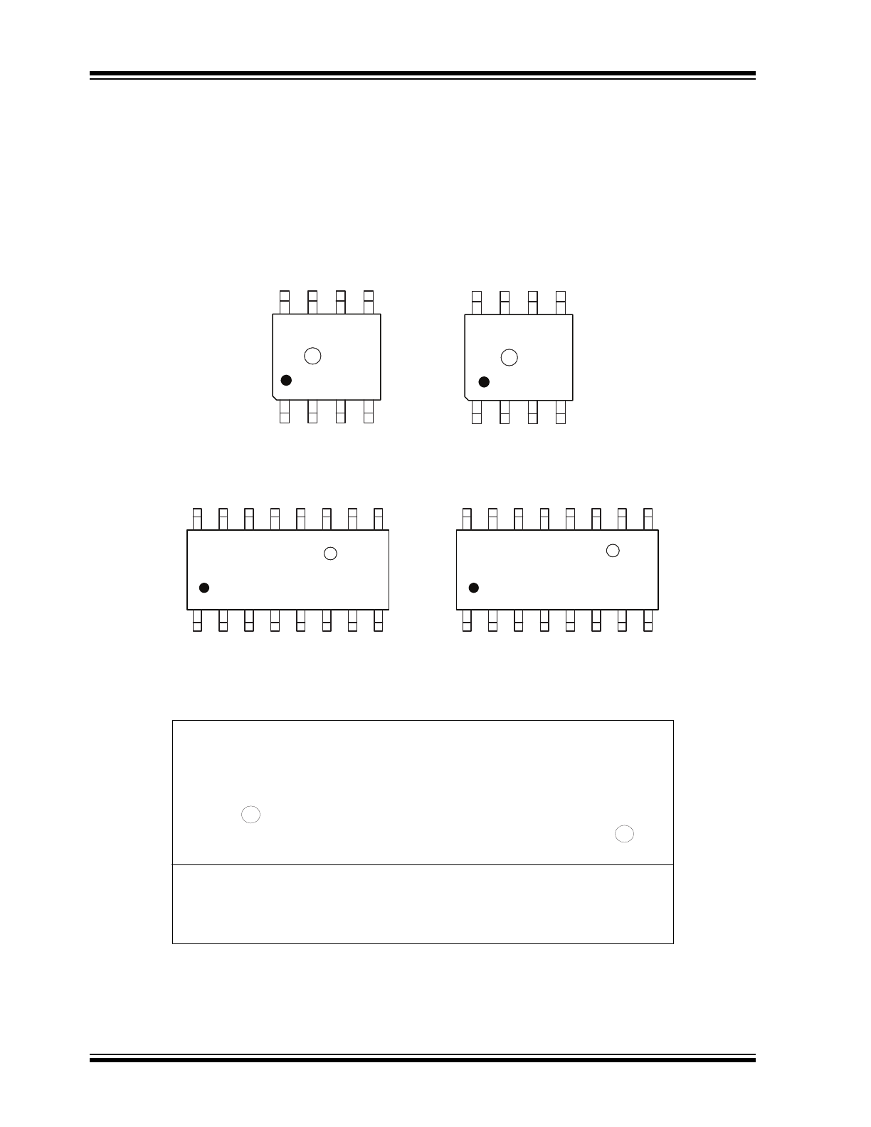
Package Type
See
Table 2-1
for pin information.
8-lead SOIC
(Top view)
16-lead SOIC
(Top view)
1
2
3
4
5
6
7
8
16
15
14
13
12
11
10
9
8
7
6
5
1
2
3
4
VIN
CS
GND
GATE
RT
DNC
VDD
DNC
VIN
DNC
DNC
CS
GND
DNC
DNC
GATE
DNC
DNC
RT
DNC
VDD
DNC
DNC
DNC
s
Switch-Dimmable LED Driver
VIN
VDD
CS
RT
GATE
HV9801A
250mV
440mV
VDD Regulator
Current Mirror from VDD Rail
Leading
Edge
Blanking
S Q
R Q
OR
Average
Current
Regulator
OFF
Time
Generator
OTP
AND
UVLO
GND
Hiccup
HV9801A
DS20005692A-page 2
2017 Microchip Technology Inc.
Functional Block Diagram
2017 Microchip Technology Inc.
DS20005692A-page 3
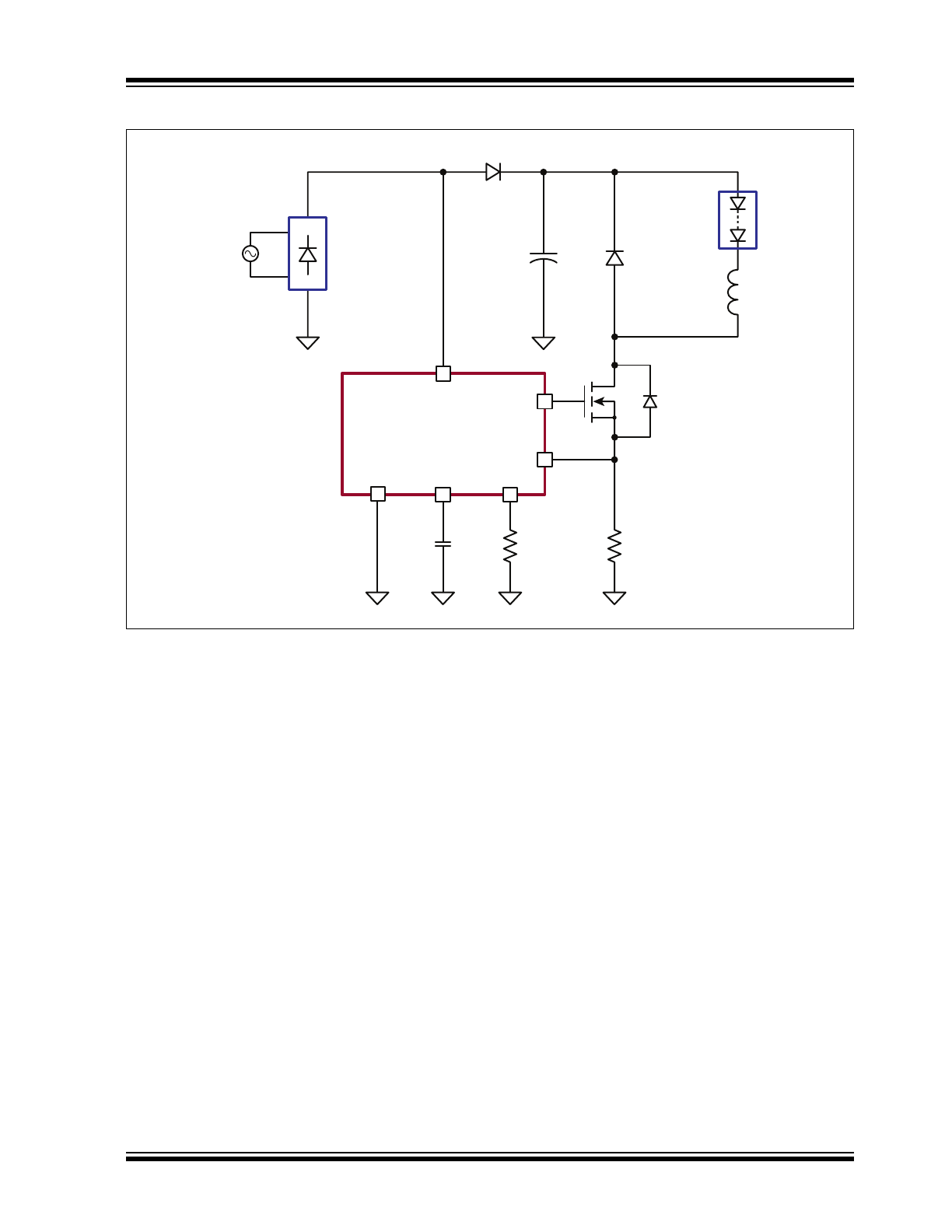
HV9801A
Typical Application Circuit
VIN
GATE
CS
GND VDD RT
HV9801A
C
DD
R
T
R
CS
L
AC
VIN
BUS
HV9801A
DS20005692A-page 4
2017 Microchip Technology Inc.
1.0
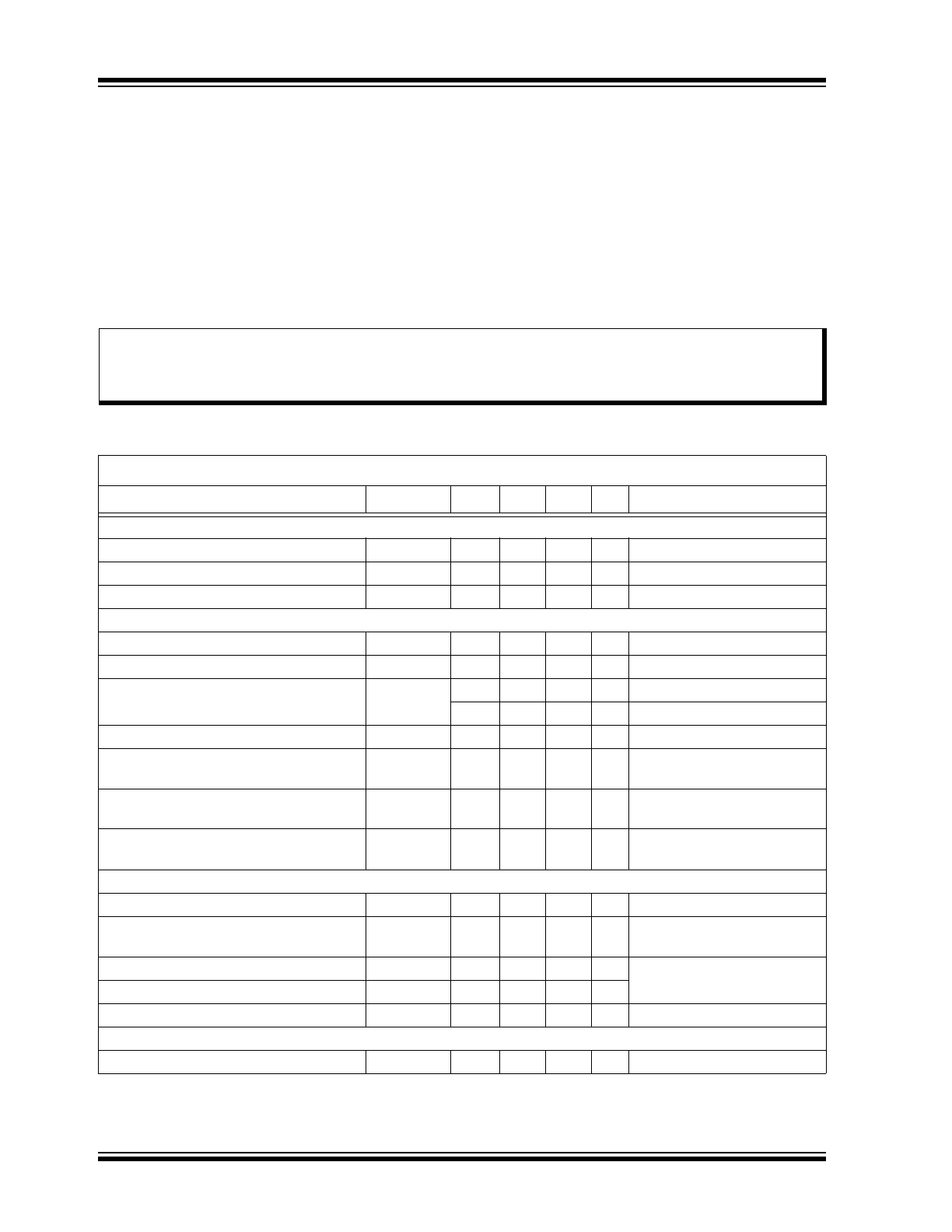
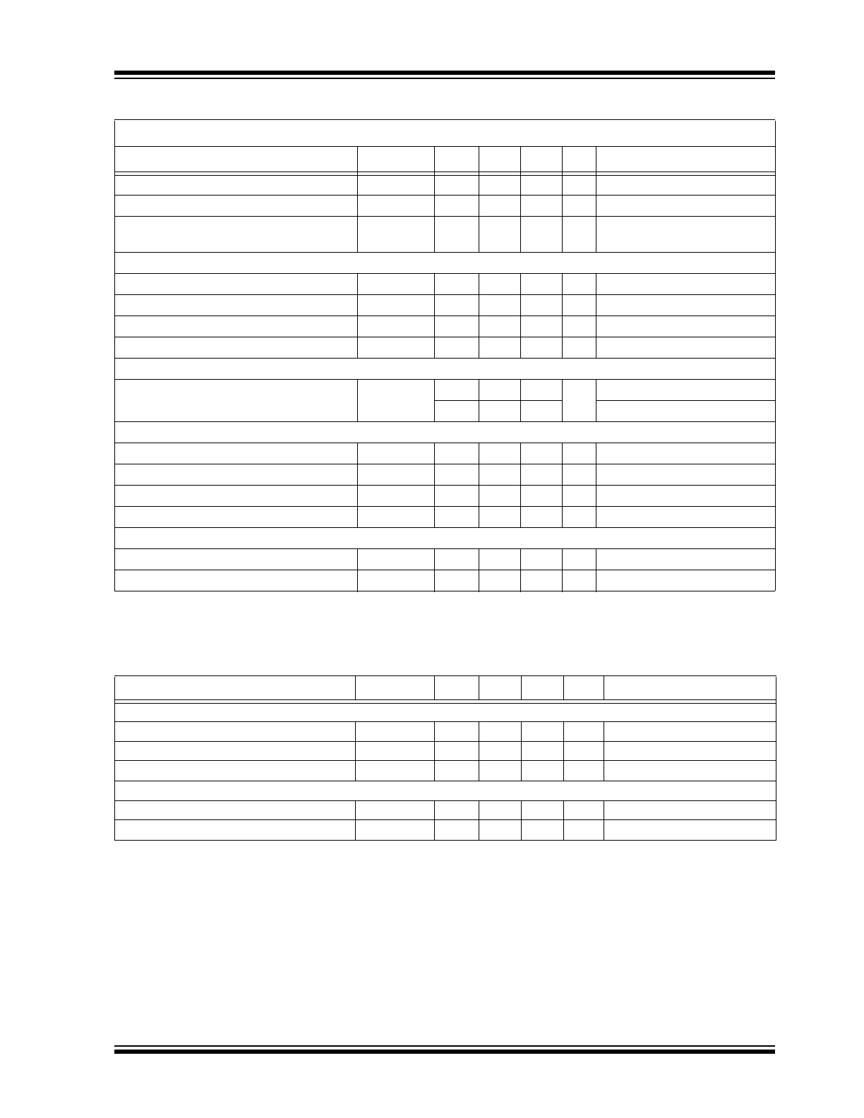
ELECTRICAL CHARACTERISTICS
Absolute Maximum Ratings†
V
IN
.......................................................................................................................................................................... 470V
V
DD
........................................................................................................................................................................... 12V
V
CS
, V
GATE
....................................................................................................................................–0.3V to (V
DD
+0.3V)
Junction Temperature Range, T
J
......................................................................................................... –40°C to +150°C
Storage Temperature Range, T
S
......................................................................................................... –65°C to +150°C
Power Dissipation (T
A
= 25 °C):
8-lead SOIC
............................................................................................................................................ 650 mW
16-lead SOIC
........................................................................................................................................ 1000 mW
† Notice: Stresses above those listed under “Absolute Maximum Ratings” may cause permanent damage to the
device. This is a stress rating only, and functional operation of the device at those or any other conditions above those
indicated in the operational sections of this specification is not intended. Exposure to maximum rating conditions for
extended periods may affect device reliability.
ELECTRICAL CHARACTERISTICS
Electrical Specifications: Specifications are at T
A
= 25°C, V
IN
= 15V unless otherwise noted.
Parameter
Sym.
Min.
Typ.
Max. Unit
Conditions
INPUT
Input Voltage
V
IN
15
—
450
V
Note 2
Input Current
I
IN
—
1
2
mA
Supply Current, OTP Shutdown
I
IN, OT
—
—
500
μA
Note 1
V
DD
REGULATOR
Undervoltage Lockout Threshold
V
UVLO
6.45
6.7
7.1
V
V
IN
rising (
Note 2
)
Undervoltage Lockout Hysteresis
∆V
UVLO
—
500
—
mV V
IN
falling
Maximum Input Current, Limited by UVLO
I
UVLO
3.5
—
—
mA T
A
= 25°C (
Note 1
)
1.5
—
—
mA T
A
= 125°C (
Note 1
)
Output Voltage
V
DD
7.25
7.5
7.75
V
C
GATE
= 500 pF, R
T
= 226 kΩ
Line Regulation
∆V
DD, LINE
—
—
1
V
V
IN
= 15V to 450V,
C
GATE
= 500 pF, R
T
= 226 kΩ
V
DD
Voltage Margin
∆V
DD(UV)
500
—
—
mV
∆V
DD(UV)
= V
DD
–V
UVLO, FALL
(
Note 2
)
Load Regulation
∆V
DD, LOAD
—
—
100
mV
I
VDD
= 0 mA to 1 mA,
C
GATE
= 500 pF, R
T
= 226 kΩ
SWITCH DIMMING
Supply Current after Power Loss
I
VDDX
—
—
700
μA
Note 2
Undervoltage Lockout during V
IN
Power Loss
V
UVLO, DIM
—
3.5
—
V
V
IN
falling
Power Loss, Qualification Time
T
PL1
—
60
—
ms V
IN
falling below V
UVLO
(
Note 1
)
Power Loss, Time to Reset
T
PL2
—
1
—
s
PWM Dimming Frequency
F
PWM
—
1.2
—
kHz
LED CURRENT REGULATOR
Current Sense Threshold
V
CST
236
250
256
mV
Note 2
Note 1: Determined by characterization; not production tested
2: Specifications apply over the full operating ambient temperature range of –40°C < T
A
< +125°C.
2017 Microchip Technology Inc.
DS20005692A-page 5
HV9801A
Leading Edge Blanking Time
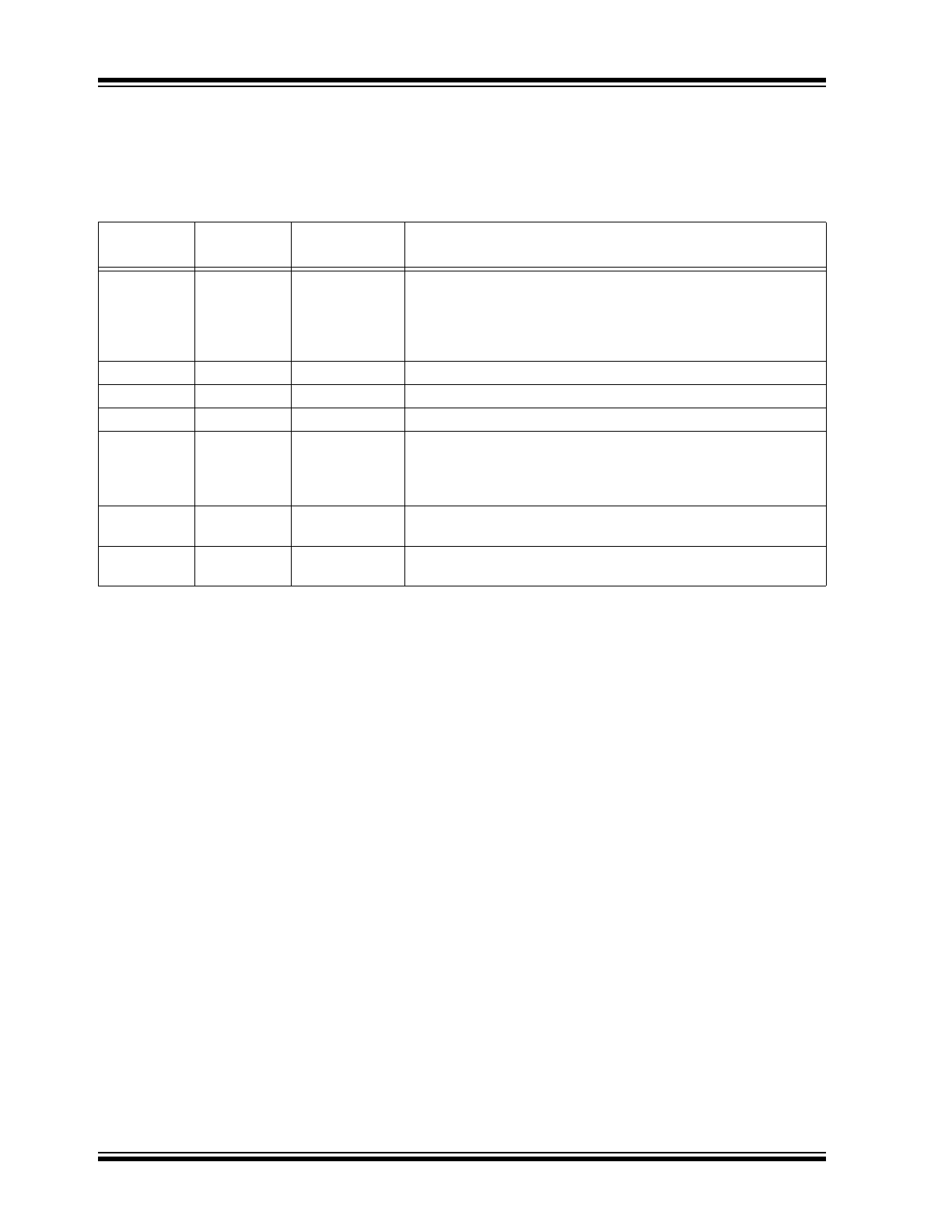
T
LEB
110
—
260
ns
Note 2
Minimum On-time
T
ONX
—
—
760
ns
V
CS
= V
CST
+ 30 mV
Maximum Duty Cycle Maintaining
Regulation
D
MAX
80
—
—
%
LED current falls beyond this
duty cycle
SHORT-CIRCUIT PROTECTION
Hiccup Threshold
V
CSH
—
440
—
mV
V
CS
High to Gate Low Delay
T
DLY
—
—
180
ns
V
CS
= V
CSH
+ 30 mV
Hiccup Time
T
SCH
—
750
—
μs
Minimum On-time
T
ONXSC
—
—
430
ns
V
CS
= V
DD
T
OFF
TIMER
Off-time
T
OFF
32
40
48
μs
R
T
= 1 MΩ
8
10
12
R
T
= 226 kΩ
GATE DRIVER
Sourcing Current
I
SRC
165
—
—
mA V
GATE
= 0V
Sinking Current
I
SINK
165
—
—
mA V
GATE
= V
DD
Rise Time
t
r
—
30
50
ns
C
GATE
= 500 pF
Fall Time
t
f
—
30
50
ns
C
GATE
= 500 pF
OVERTEMPERATURE PROTECTION
Trip Temperature
T
TRIP
—
140
—
°C
Note 1
Hysteresis
∆T
TRIP
—
20
—
°C
Note 1
TEMPERATURE SPECIFICATIONS
Parameter
Sym.
Min.
Typ.
Max.
Unit
Conditions
TEMPERATURE RANGE
Operating Ambient Temperature
T
A
–40
—
+125
°C
Maximum Junction Temperature
T
J
–40
—
+150
°C
Storage Temperature
T
S
–65
—
+150
°C
PACKAGE THERMAL RESISTANCE
8-lead SOIC
JA
—
101
—
°C/W
16-lead SOIC
JA
—
83
—
°C/W
ELECTRICAL CHARACTERISTICS (CONTINUED)
Electrical Specifications: Specifications are at T
A
= 25°C, V
IN
= 15V unless otherwise noted.
Parameter
Sym.
Min.
Typ.
Max. Unit
Conditions
Note 1: Determined by characterization; not production tested
2: Specifications apply over the full operating ambient temperature range of –40°C < T
A
< +125°C.
HV9801A
DS20005692A-page 6
2017 Microchip Technology Inc.
2.0
PIN DESCRIPTION
The details on the pins of HV9801A are listed on
Table 2-1
. See location of pins in
Package Types
.
TABLE 2-1:
PIN FUNCTION TABLE
Pin Name
8-lead SOIC
Pin Number
16-lead SOIC
Pin Number
Description
VIN
1
1
Connect to bridge rectifier output. Supplies power to the V
DD
regulator. Detects light switch power-off event through loss of
bridge rectifier output voltage. Do not connect excessive capaci-
tance before or after the bridge to allow V
IN
to drop rapidly after
loss of power.
CS
2
4
Current sense input
GND
3
5
Ground
GATE
4
8
Gate driver output
VDD
6
12
V
DD
regulator output. Connect a high-frequency bypass and a
hold-up capacitor at V
DD
. Bypass capacitor to be 100 nF minimum.
See
Section 3.0 “Application Information”
for hold-up capaci-
tance.
RT
8
14
Off-time programming input. Connect programming resistor to
GND.
DNC
5, 7
2, 3, 6, 7, 9, 10,
11, 13, 15, 16
Stands for “Do Not Connect.”
2017 Microchip Technology Inc.
DS20005692A-page 7
HV9801A
3.0
APPLICATION INFORMATION
3.1
Current Control
3.1.1
CONTINUOUS CONDUCTION
MODE (CCM)
The HV9801A is designed to control a buck converter
operating in CCM.
Continuous Conduction Mode operation is
characterized by converter operation with non-zero
inductor current throughout the switching cycle. Such
operation can be achieved by proper selection of the
inductance.
3.1.2
LED CURRENT
The HV9801A regulates the LED current with an
accuracy far superior to that of competing Peak Current
mode controllers.
Average LED current is set by the current sense
resistor R
CS
and the current regulator reference
voltage. See
Equation 3-1
and
Equation 3-2
.
EQUATION 3-1:
V
I R
=
EQUATION 3-2:
250mV
I
LED
R
CS
=
For example, a 2Ω resistor corresponds to a 125 mA
(average) LED current.
3.1.3
CURRENT CONTROL
PERFORMANCE
The control method of the HV9801A virtually eliminates
the regulation errors associated with Peak Current
mode controllers, such as errors caused by inductor
tolerance, propagation delay of the current sense
comparator, tolerance in the oscillator frequency or
off-timer and changes in line and load voltage.
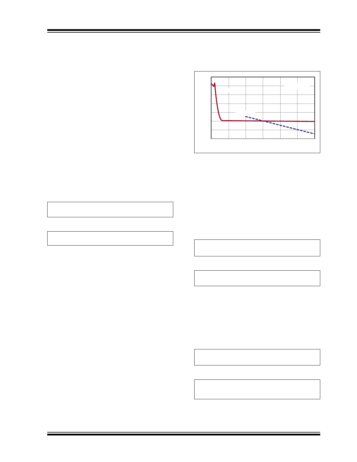
Figure 3-1
compares the load regulation of the
HV9801A and that of a device with peak current
control. The graph clearly shows the difference in load
regulation between the HV9801A and the HV9910B,
which is a peak current regulator.
0.60
0.55
0.50
0.45
0.40
0.35
0.30
0.25
0 10 20 30 40 50 60
HV9910B
HV9801A
V
IN
= 170VDC
Output Voltage, V
LED Current,
A
FIGURE 3-1:
Output Characteristics of the
HV9801A LED Driver.
3.2
Duty Cycle, Off-time, On-time and
Inductor
3.2.1
DUTY CYCLE
The duty cycle (D) is related to the load voltage (V
LED
)
and input voltage (V
BUS
) by the simple relation shown
in
Equation 3-3
and
Equation 3-4
.
EQUATION 3-3:
V
OUT
D V
IN
=
EQUATION 3-4:
V
LED
D V
BUS
=
3.2.2
OFF-TIME
The HV9801A operates with constant off-time control,
which avoids subharmonic oscillation.
Switching period and switching frequency are related to
on-time and off-time as shown in
Equation 3-5
and
Equation 3-6
.
EQUATION 3-5:
T
SW
T
ON
T
OFF
+
=
EQUATION 3-6:
F
SW
1
T
SW
----------
=
HV9801A
DS20005692A-page 8
2017 Microchip Technology Inc.
On-time is related to off-time and duty cycle. See
Equation 3-7
.
EQUATION 3-7:
D
T
ON
T
ON
T
OFF
+
-----------------------------------
=
T
ON
D 1 D
–
T
OFF
=
With a given T
OFF
, the HV9801A dynamically adjusts
T
ON
to regulate the LED current. Specifically, T
ON
adapts to the duty cycle associated with the given V
BUS
and V
LED
.
3.2.3
OFF-TIME PROGRAMMING
Off-time is programmed by the R
T
resistor as illustrated
in
Equation 3-8
.
EQUATION 3-8:
T
OFF
A R
T
B
+
=
Where: A = 40 ps / Ω and B = 300 ns
For instance, a 200 kΩ resistor corresponds to 8.3 μs
off-time.
An acceptable range for R
T
is 30 kΩ to 1 MΩ,
corresponding to an off-time range between 1.5 µs and
40.3 µs.
3.2.4
INDUCTOR
Because the converter should operate in CCM, the
inductor current should not fall to zero within a
switching cycle and the inductor current ripple should
be sized accordingly.
A common choice for peak-to-peak inductor current
ripple (PPR) is 30% to 40% of nominal LED current.
Inductance can be calculated from the current drop
during off-time as shown in
Equation 3-9
and
Equation 3-10
.
EQUATION 3-9:
L
I
V
T
=
EQUATION 3-10:
L PPR I
LED
V
LED
T
OFF
=
For example, 30% PPR on 350 mA average current
equates to 105 mA ripple, which together with 5 µs
off-time and 30V LED string voltage corresponds to
1.43 mH inductance.
A design with 30V LED voltage and 150V bus voltage
corresponds to a 20% duty cycle, while a 120V bus
voltage coincides with a 25% duty cycle. A 20% duty
cycle corresponds to 1.25 µs on-time, and a 25% duty
cycle corresponds to 1.67 µs on-time. Hence, the
switching frequency is 160 kHz at 150V bus voltage
and 150 kHz at 120V bus voltage.
3.2.5
MAXIMUM DUTY CYCLE
Duty cycle should be limited to the specified maximum
of 80%. Accordingly, the targeted LED string voltage
and the bus voltage are limited to the same ratio.
Operation at a larger desired duty cycle than the
maximum duty cycle results in an LED current lower
than programmed.
3.2.6
MINIMUM DUTY CYCLE
Duty cycle is limited on the low side by the minimum
on-time specification (760 ns). Operation at a smaller
desired on-time than the minimum causes the LED
current to exceed the programmed value.
LED string voltage cannot be made arbitrarily low.
Minimum LED string voltage can be determined with
Equation 3-11
.
EQUATION 3-11:
D
MIN
T
ONX
T
OFF
T
ONX
+
--------------------------------------
=
V
LED
D
MIN
V
BUS
=
For instance, with 5 µs off-time, the duty cycle should
be kept above 13%. Such a duty cycle corresponds to
an LED string voltage of 19.5V at 150V bus voltage.
A design that needs a lower LED string voltage
requires a longer off-time.
3.2.7
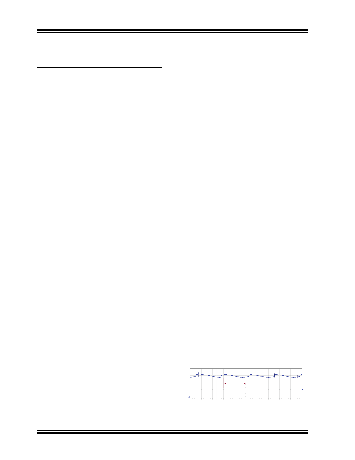
SHORT-CIRCUIT PROTECTION
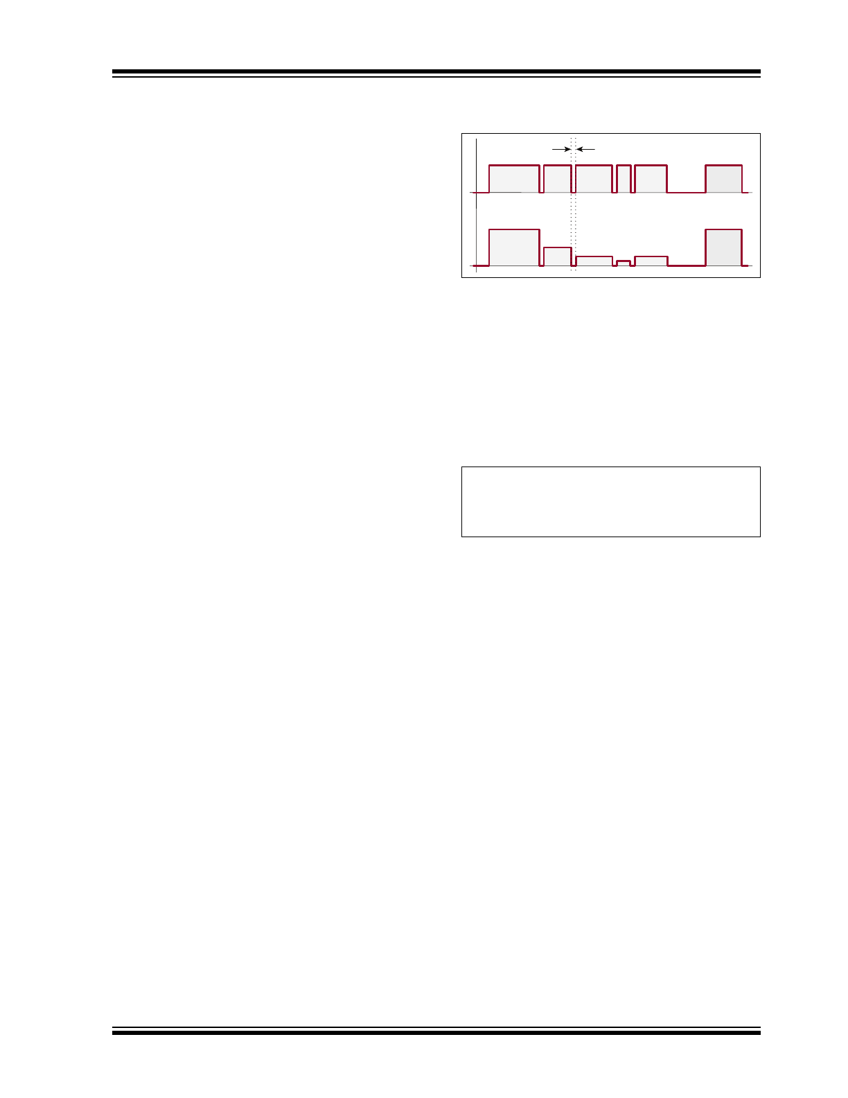
An increase in the LED current sense signal above
440 mV (176% of nominal) trips the short-circuit
comparator, thereby causing the converter to switch to
Hiccup mode. In Hiccup mode, off-time is lengthened to
about 750 µs to allow the inductor current to drop to a
safe level.
Without the extended off-time, the inductor current
increases with every switching cycle, causing an
overcurrent damage to the converter.
The off-time extension can be observed in
Figure 3-2
below.
~750µs
440mV/R
CS
S
FIGURE 3-2:
Short-circuit Inductor
Current.
2017 Microchip Technology Inc.
DS20005692A-page 9
HV9801A
3.2.8
LEADING EDGE BLANKING
The MOSFET drain current and the current sense
signal exhibit a spike at the start of a switching cycle,
which arises from the MOSFET gate charging current
and the current required for discharging the MOSFET
drain node. These two currents typically exceed the
inductor by quite a margin.
The current sense signal is blanked at the start of the
switching cycle in order to avoid a premature trigger of
the current sense and the short-circuit protection
comparators.
3.2.9
V
DD
REGULATOR
The V
DD
regulator generates a source of regulated
voltage for operation of internal and external circuits
from the power applied at the V
IN
pin. Alternatively, the
V
DD
voltage can be supplied from a source directly
connected to the V
DD
pin.
3.3
Switch Dimming
3.3.1
GENERAL
Lamp brightness can be adjusted to one of four
discrete levels by rapidly cycling power with the light
switch. The brightness levels are traversed in an
up-and-down manner, the four levels being 100%,
50%, 25% and 12.5%. Brightness resumes at the
highest level when power is removed for more than a
second.
Reduction of LED current is accomplished through
PWM dimming with a PWM dimming frequency of
about 1 kHz. The PWM frequency is generated by an
internal oscillator, and the PWM duty cycle is controlled
by digital logic.
Turning the light switch off and on within one second
adjusts LED current to the next level in each dimming
step. The direction of dimming depends on the existing
position in the dimming sequence. The illustration in
Figure 3-3
shows more details. The sequence starts at
100% and adjusts to the next lower level by the first
dimming step and then adjusts to the next lower level
by the next dimming step. Upon reaching the lowest or
highest level, the direction of the sequence reverses.
Therefore, the actual overall dimming sequence is
100%, 50%, 25%, 12.5%, 25%, 50%, 100%, and the
sequence repeats as the dimming steps continue.
When power is removed for more than one second, the
dimming sequence is terminated and the brightness is
reset to 100% upon turn-on of the light switch.
OFF/ON cycle time 1second (max.)
100%
50%
25% 12.5% 25%
100%
Brightness
AC Line Power
ON
FIGURE 3-3:
LED Brightness and AC
Line Power.
3.3.2
V
DD
CAPACITOR
The V
DD
voltage should be maintained for at least one
second and above the 3.5V level after loss of V
IN
power
to allow certain timing circuits to function.
The minimum V
DD
capacitance required can be
calculated with
Equation 3-12
.
EQUATION 3-12:
C
V
I
T
=
C
DD
7.5V 3.5V
–
I
VDDX
1s
=
With 700 µA of I
VDDX
the bypass capacitance should be
175 µF.
3.3.3
DETECTION OF POWER CYCLING
The presence of AC line power is detected at the V
IN
pin. To this end, loss of AC power should result in a
rapidly falling voltage at the output of the bridge
rectifier.
The V
IN
voltage drops due to the current draw from the
V
DD
regulator. In order to facilitate a quick drop in
voltage, a diode should be added to isolate the bus
capacitor from the V
IN
pin as shown in the
Typical
Application Circuit
.
HV9801A
DS20005692A-page 10
2017 Microchip Technology Inc.
4.0
PACKAGING INFORMATION
4.1
Package Marking Information
Legend: XX...X
Product Code or Customer-specific information
Y
Year code (last digit of calendar year)
YY
Year code (last 2 digits of calendar year)
WW
Week code (week of January 1 is week ‘01’)
NNN
Alphanumeric traceability code
Pb-free JEDEC
®
designator for Matte Tin (Sn)
*
This package is Pb-free. The Pb-free JEDEC designator ( )
can be found on the outer packaging for this package.
Note:
In the event the full Microchip part number cannot be marked on one line, it will
be carried over to the next line, thus limiting the number of available
characters for product code or customer-specific information. Package may or
not include the corporate logo.
3
e
3
e
8-lead SOIC
Example
NNN
XXXXXXXX
YYWW
e3
991
HV9801A
1727
LG
XX
e3
16-lead SOIC
XXXXXXXX
YYWWNNN
e3
Example
HV9801ANG
1711541
e3