
2017 Microchip Technology Inc.
DS20005689A-page 1
HV9150
Features
• 6V to 500V Wide Output Voltage Range
• 2.7V Low Input Voltage
• 5W Maximum Output Power with External
MOSFET Driver
• Built-in Charge Pump Converter for the Gate
Driver
• Programmable Switching Frequency from 40 kHz
to 400 kHz
• Four Programmable Duty Cycles from 50% to
87.5%
• FB Return Ground Switch for Power Saving
Applications
• Built-in Delay Timer for Internal Protection
• Non-isolated DC/DC Converter
Applications
• Portable Electronic Equipment
• MEMS
• Printers
General Description
The HV9150 is a high output voltage Hysteretic mode
step-up DC/DC controller that has a built-in charge
pump converter and a linear regulator for a wide range
of input voltage. The Charge Pump Converter mode is
ideal for battery-powered applications. The internal
converter can provide a minimum of 5V gate driver
output voltage (at V
IN
= 2.7V) to the external N-channel
MOSFET. The range of 2.7V to 4.5V input supply
voltage is ideal for battery-powered applications, such
as portable electronic equipment. The internal linear
regulator is selected when a higher supply voltage rail
is available in the system.
A feedback return ground path switch is also integrated
into the device to minimize the quiescent current during
the controller shutdown. This feature provides power
savings for energy-critical applications.
In addition, a built-in timer is available to protect the
internal circuit and help dissipate the energy from the
external high-voltage storage capacitor. This device is
designed for systems requiring high-voltage and
low-current applications such as MEMS devices.
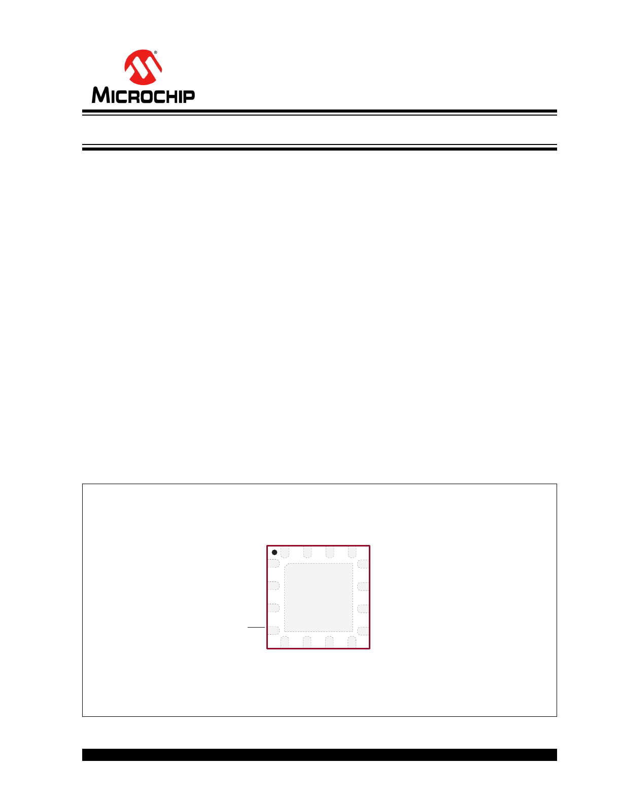
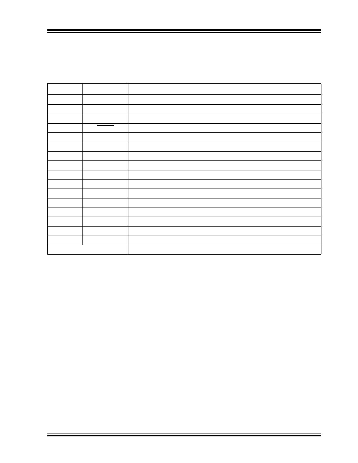
Package Type
Pads are at the bottom of the package. Center heat slug is at ground potential. See
Table 3-1
for pin information.
16-lead QFN
(Top View)
VDD
GATE
FB_RTN
FB
VCONTROL
FREQ_ADJ
EXT_REF
CT
VLL
GND
EN
CP_EN
CCP1-
CCP1+
CCP2-
CCP2+
1
16
High-Voltage Output Hysteretic-Mode Step-Up DC/DC Controller
Delay
OSC
3x Charge Pump
Converter
LDO
VREF
- +
Hysteretic Mode
Controller
V
DD
V
DD
V
LL
V
LL
V
LL
V
LL
CCP1+/-
CCP2+/-
VDD
VLL
GND
CT
EN
FREQ_ADJ
VCONTROL
(Duty Cycle Adj)
CP_EN
GATE
EXT_REF
FP_RTN
FB
LDO
Mode
CP
Mode
HV9150
DS20005689A-page 2
2017 Microchip Technology Inc.
Functional Block Diagram
2017 Microchip Technology Inc.
DS20005689A-page 3
HV9150
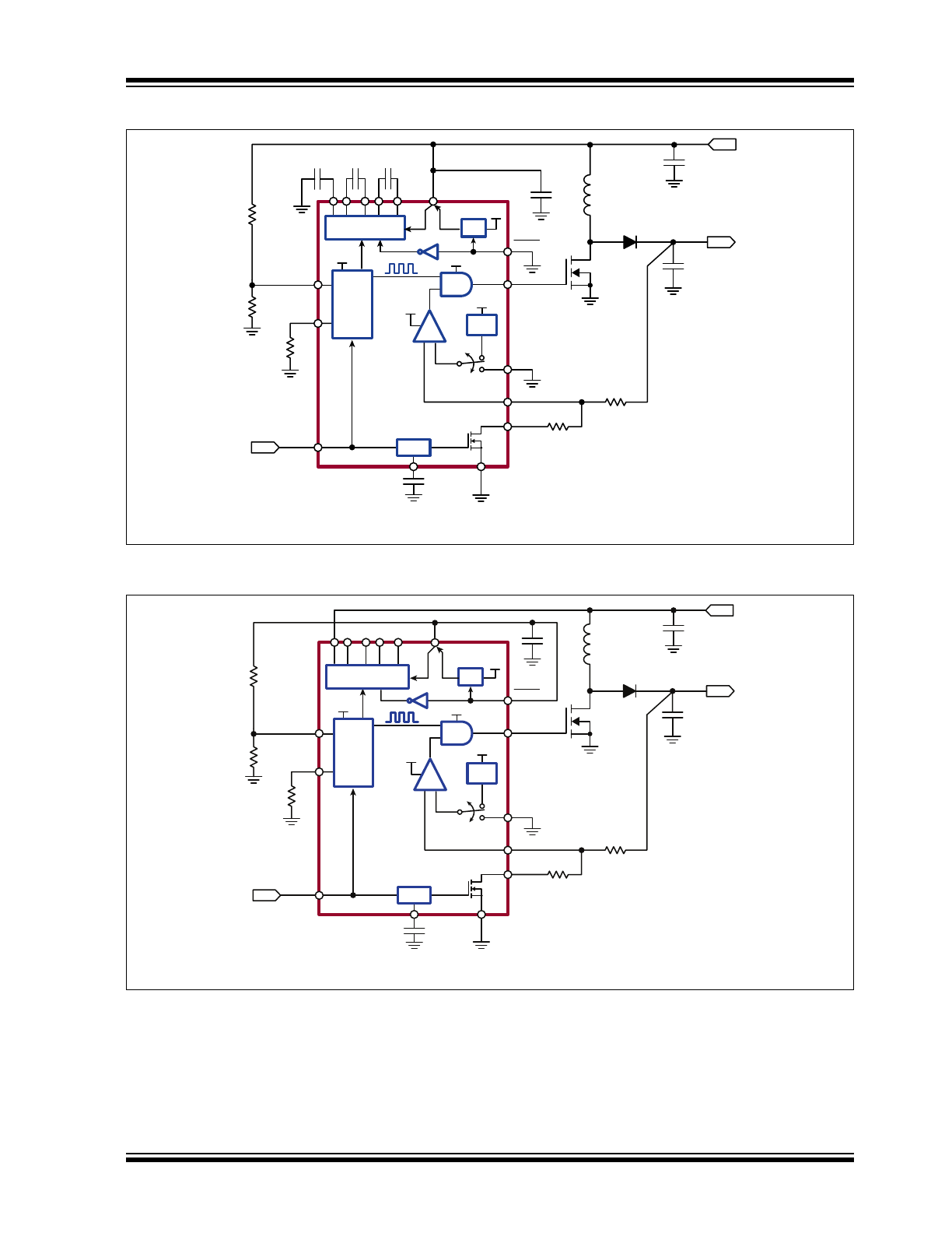
Typical Application Circuits
CCP2±
0.22μF
R
FREQ
V
OUT
6.0 - 500V
V
IN
2.7 - 4.5V
GND
R
1
R
2
L
CT
Delay
OSC
VREF
3x Charge Pump
Converter
LDO
CCP1±
0.22μF
VDD
0.22μF
VLL
1.0μF
CP_EN
- +
V
LL
V
LL
V
LL
V
DD
GATE
EXT_REF
FB_RTN
FB
EN
FREQ_ADJ
VCONTROL
0V/3.3V
V
DD
LDO
Mode
CP
Mode
Charge Pump (CP) Mode
Linear Regulator (LDO) Mode
CCP2±
R
FREQ
V
OUT
15 - 500V
V
IN
5.0 - 12V
GND
R
1
R
2
L
CT
Delay
OSC
VREF
3x Charge Pump
Converter
LDO
CCP1±
VDD
VLL
CP_EN
- +
V
LL
V
LL
V
LL
V
DD
GATE
EXT_REF
FB_RTN
FB
EN
FREQ_ADJ
VCONTROL
0V/3.3V
V
DD
1.0μF
LDO
Mode
CP
Mode
HV9150
DS20005689A-page 4
2017 Microchip Technology Inc.
1.0
ELECTRICAL CHARACTERISTICS
Absolute Maximum Ratings†
Input Voltage Supply, V
LL
........................................................................................................................... –0.5V to +5V
Charge Pump Output Voltage, V
DD
....................................................................................................... –0.5V to +13.6V
Logic Input Levels ............................................................................................................................. –0.5V to V
LL
+0.5V
Operating Ambient Temperature, T
A
................................................................................................... –25°C to +125°C
Storage Temperature, T
S
...................................................................................................................... –65°C to +150°C
Continuous Power Dissipation (On a 3 x 4-inch FR4 PCB at T
A
= 25°C):
16-lead QFN .......................................................................................................................................... 3000 mW
† Notice: Stresses above those listed under “Absolute Maximum Ratings” may cause permanent damage to the
device. This is a stress rating only, and functional operation of the device at those or any other conditions above those
indicated in the operational sections of this specification is not intended. Exposure to maximum rating conditions for
extended periods may affect device reliability.
RECOMMENDED OPERATING CONDITIONS
Parameter
Sym.
Min.
Typ.
Max.
Unit
Conditions
Input Voltage (CP Mode)
V
LL
2.7
—
4.5
V
High-level Input Voltage
V
IH
0.8 V
LL
—
V
LL
V
Low-level Input Voltage
V
IL
0
—
0.2 V
LL
V
DC ELECTRICAL CHARACTERISTICS
Electrical Specifications: Over recommended operating supply voltages and temperatures; unless otherwise noted,
T
J
= 25°C.
Parameter
Sym.
Min.
Typ.
Max.
Unit
Conditions
POWER SUPPLY
Quiescent V
LL
Supply Current
(EN = ‘0’)
I
LLQ(off)
—
—
2
μA
VLL Supply Current
(EN = ‘1’)
GATE = NC
I
LL(on)
—
—
1.5
mA
f
OSC
= 100 kHz, V
LL
= 4.5V
GATE = 300 pF
—
—
4
VDD Supply Current
(EN = ‘1’)
GATE = NC
I
DD(on)
—
—
1
mA
f
OSC
= 100 kHz, V
DD
= 12.6V
GATE = 300 pF
—
—
2.5
Quiescent VDD Supply Current
(EN = ‘0’)
I
DDQ(off)
—
—
2
μA
High-level Logic Input Current
I
IH
—
—
1
μA
V
IH
= V
LL
Low-level Logic Input Current
I
IL
—
—
–1
μA
V
IL
= 0V
Gate Driver Output
Voltage
V
LL
= 4.5V
GATE = NC
GATE
10.2
—
12.3
V
V
LL
= 2.7V
GATE = NC
5
—
6.9
Linear Regulator Output Voltage
V
LL(LDO)
3
—
3.6
V
2017 Microchip Technology Inc.
DS20005689A-page 5
HV9150
AC ELECTRICAL CHARACTERISTICS
Electrical Specifications: Over recommended operating supply voltages and temperatures; unless otherwise noted
T
J
= 25°C.
Parameter
Sym.
Min.
Typ.
Max.
Unit
Conditions
FEEDBACK (FB)
Internal Feed-
back Reference
Voltage
Accuracy
V
REF
1.22
1.25
1.28
V
Range
1.2
1.25
1.3
T
A
= –25 to 85°C
Input Bias Current
I
BIAS
—
—
1
μA
EXT_REF is selected.
External
Reference
Voltage
Range
EXT_REF
0
—
V
LL
–1.4
V
Trigger INT
Reference
0
—
0.12
V
During EN positive triggering
Trigger EXT
Reference
0.5
—
V
LL
–1.4
V
On-resistance, R
DS
FB_RTN
—
—
500
Ω
I
O
= 2 mA
Breakdown Voltage, BV
—
—
13.5
V
GATE DRIVER OUTPUT (GATE)
Rise Time
t
r
—
—
36
ns
C
L
= 300 pF, V
DD
= 12V
Fall Time
t
f
—
—
12
ns
Pull-up
Resistance
V
DD
= 5V
R
UP
—
—
45
Ω
I
O
= 20 mA
V
DD
= 12V
—
—
30
I
O
= 50 mA
Pull-down
Resistance
V
DD
= 5V
R
DOWN
—
—
15
Ω
I
O
= 20 mA
V
DD
= 12V
—
—
12
I
O
= 50 mA
Oscillator Frequency
f
GATE
—
½ f
OSC
—
kHz
CHARGE PUMP CONVERTER
Charge Pump Output Voltage
V
DD
5
3 V
LL
–1.8
12.6
V
2.7V ≤ V
LL
≤ 4.5V
C
CP1
= 220 nF
C
CP2
= 220 nF
C
CP3
= 220 nF
Oscillator
Frequency
Accuracy
f
OSC
170
195
220
kHz
R
FREQ
= 270 kΩ, V
LL
= 3.3V
Range
40
—
400
Over R
FREQ
range
Oscillator Frequency Tolerance
∆f
—
15
—
%
50 kHz ≤ f
OSC
≤ 250 kHz
Duty Cycle
Accuracy
DC
86
87.5
9
%
R
FREQ
= 270 kΩ
Range
—
0
—
%
0 < V
CNTL
≤ 0.18 V
LL
—
50
—
%
0.22 V
LL
< V
CNTL
≤ 0.38 V
LL
—
62.5
—
%
0.42 V
LL
< V
CNTL
≤ 0.58 V
LL
—
75
—
%
0.62 V
LL
< V
CNTL
≤ 0.78 V
LL
—
87.5
—
%
0.82 V
LL
< V
CNTL
≤ V
LL
Duty Cycle Adjustment
V
CONTROL
0
—
V
LL
V
See
Table 4-2
.
Frequency Adjustment Resistor
R
FREQ
120k
—
1.2M
Ω
Maximum Charge
Pump Output
Resistance
Pull-up
R
CP
—
—
20
Ω
V
LL
= 2.7V, I
O
= 10 mA
Pull-down
—
—
20
HV9150
DS20005689A-page 6
2017 Microchip Technology Inc.
FIGURE 1-1:
Duty Cycle Selection Hysteresis at V
CONTROL
Pin at 25°C.
Output Ripple at V
DD
V
RIPPLE
—
—
100
mV
2.7V ≤ V
LL
≤ 4.5V
f
OSC
= 200 kHz
C
CP1
= 220 nF
C
CP2
= 220 nF
C
CP3
= 220 nF
C
GATE
= 300 pF
BW = 20 MHz
DELAY TIMER
Shutdown Delay Timer
t
DELAY
—
240
—
ms
C
T
= 1 μF
TEMPERATURE SPECIFICATIONS
Parameter
Sym.
Min.
Typ.
Max.
Unit
Conditions
TEMPERATURE RANGE
Operating Ambient Temperature
T
A
–25
—
+125
°C
Storage Temperature
T
S
–65
—
+150
°C
PACKAGE THERMAL RESISTANCE
16-lead QFN
JA
—
33
—
°C/W
100
90
80
70
60
50
40
30
20
10
0
V
CONTROL
from Max to Min
V
CONTROL
from Min to Max
P
e
rc
e
nt
a
ge
of
V
LL
82%
62%
42%
22%
78%
58%
38%
18%
87.5% Duty Cycle
75% Duty Cycle
62.5% Duty Cycle
50% Duty Cycle
0% Duty Cycle
87.5% Duty Cycle
75% Duty Cycle
62.5% Duty Cycle
50% Duty Cycle
0% Duty Cycle
AC ELECTRICAL CHARACTERISTICS (CONTINUED)
Electrical Specifications: Over recommended operating supply voltages and temperatures; unless otherwise noted
T
J
= 25°C.
Parameter
Sym.
Min.
Typ.
Max.
Unit
Conditions
2017 Microchip Technology Inc.
DS20005689A-page 7
HV9150
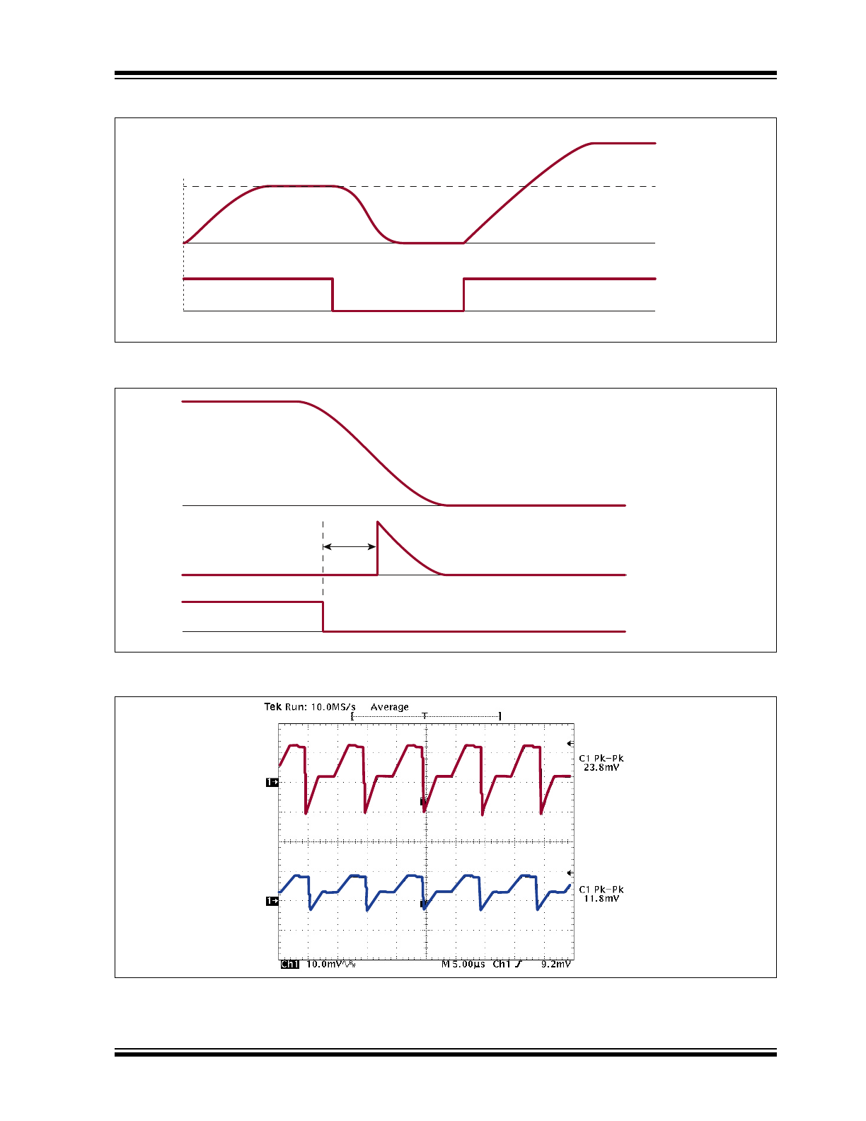
Timing Waveforms
Initial power up
X
QWV
"*GZVaTGH+
X
QWV
"*KPVaTGH+
2X
X
KJ
X
KN
XQWV
GP
FIGURE 1-2:
Enabling to use the External Voltage Reference.
t
DELAY
2X
2X
X
KJ
X
KN
XQWV
HDaTVP
GP
FIGURE 1-3:
Delay Time at FB_RTN.
V
IN
= 4.5V
V
IN
= 2.7V
FIGURE 1-4:
VCP Noise.
HV9150
DS20005689A-page 8
2017 Microchip Technology Inc.
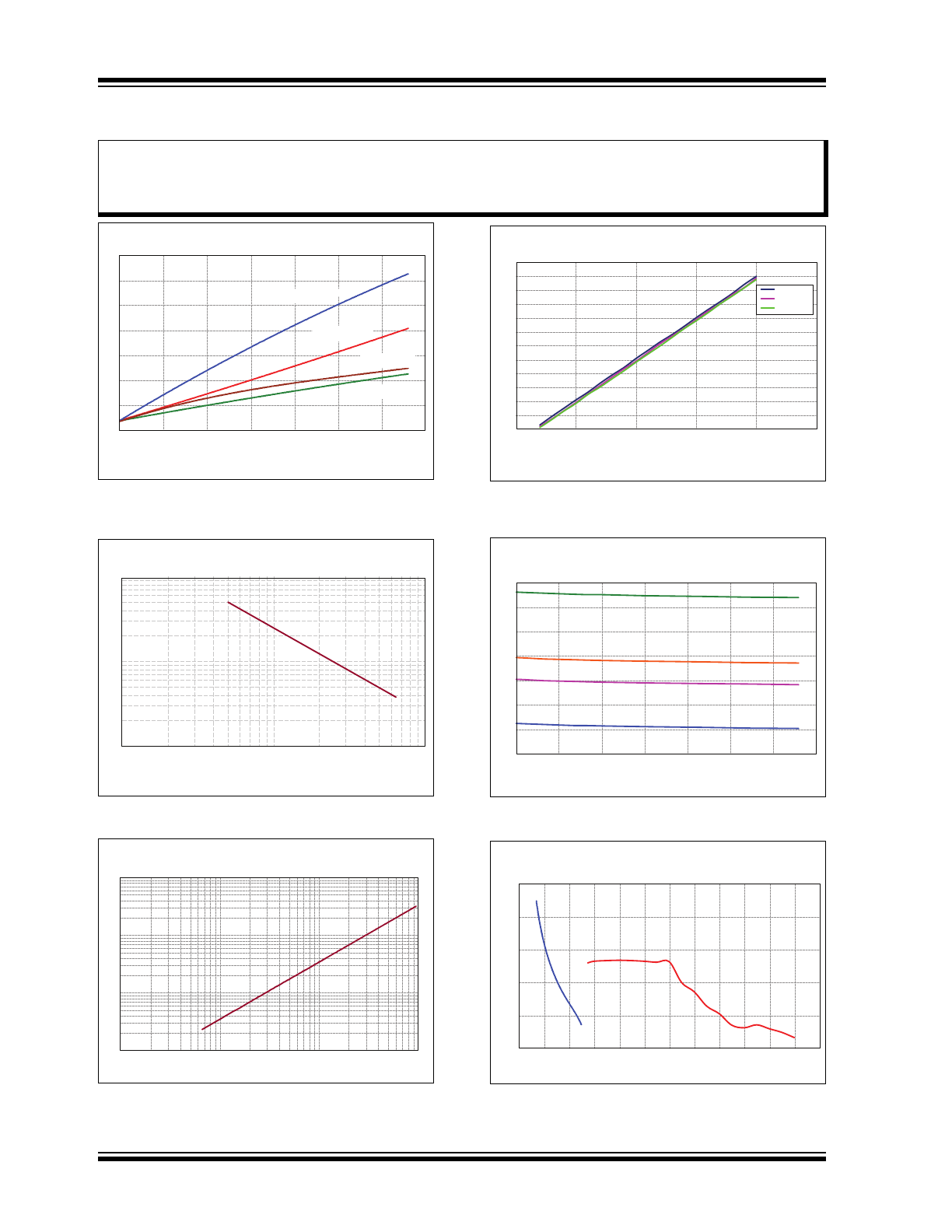
2.0
TYPICAL PERFORMANCE CURVES
35
30
25
20
15
10
5
0
0 50 100 150 200 250 300 350
T
ime (ns)
Load Capacitance (pF)
Rise time t
r
, V
DD
= 11V
(CP mode)
Fall time t
f
, V
DD
= 11V
(CP mode)
Rise time t
r
, V
DD
= 5V
(LDO mode)
Fall time t
f
, V
DD
= 5V
(LDO mode)
Note:
The graphs and tables provided following this note are a statistical summary based on a limited number of
samples and are provided for informational purposes only. The performance characteristics listed herein
are not tested or guaranteed. In some graphs or tables, the data presented may be outside the specified
operating range (e.g. outside specified power supply range) and therefore outside the warranted range.
FIGURE 2-1:
Gate Driver Rise Time (t
r
)
and Fall Time (t
f
) vs. Load Capacitance at
25°C.
1000
100
10
10
100
1000
Frequency (kHz)
R
FREQ
(kΩ)
(V
IN
= 3.3V at 25
O
C)
FIGURE 2-2:
f
GATE
vs. R
FREQ
.
100
10
1
0.1
10
100
1000
10000
Capacitance (µF)
Delay (ms)
FIGURE 2-3:
C
T
Capacitor Value vs.
Delay Time at 25°C.
12.0
11.0
10.0
9.0
8.0
7.0
6.0
2.5 3.0 3.5 4.0 4.5 5.0
Charge Pump Output V
oltage V
DD
(V)
Input Voltage V
LL
(V)
CL = 100 pF
CL = 220 pF
CL = 330 pF
FIGURE 2-4:
Charge Pump Output
Voltage vs. Input Voltage at 25°C.
12
11
10
9
8
7
6
5
0 50 100 150 200 250 300 350
Output V
oltage V
DD
(V)
Load Capacitance (pF)
(f
GATE
= 100 kHz, C
CP1
= C
CP2
= 0.22 µF, C
VDD
= 1.0 µF)
V
LL
= 4.5V
V
LL
= 3.6V
V
LL
= 3.3V
V
LL
= 2.7V
FIGURE 2-5:
Charge Pump Output
Voltage vs. Load Capacitance at 25°C.
101
100
99
98
97
96
2 3 4 5 6 7 8 9 10 11 12 13 14
Frequency (kHz)
V
LL
Input Voltage (V)
LDO mode
CP mode
(Gate output load capacitance = 330 pF, R
FREQ
= 255 kΩ @ 25
O
C)
FIGURE 2-6:
Gate Driver Switching
Frequency vs. V
LL
Input Voltage.
2017 Microchip Technology Inc.
DS20005689A-page 9
HV9150
3.0
PIN DESCRIPTION
The details on the pins of HV9150 16-lead QFN are
listed on
Table 3-1
. Refer to
Package Type
for the
location of pins.
TABLE 3-1:
PIN FUNCTION TABLE
Pin Number
Pin Name
Description
1
VLL
Input supply voltage
2
GND
Ground connection
3
EN
Enable
4
CP_EN
Charge pump/LDO enable input
5
VCONTROL
Duty cycle adjustment voltage control input
6
FREQ_ADJ
Frequency adjustment
7
EXT_REF
External reference voltage input
8
CT
Timing capacitor
9
FB
Feedback input voltage
10
FB_RTN
Feedback return
11
GATE
Gate control output
12
VDD
Charge pump output voltage
13
CCP2+
Charge pump storage capacitor #2 plus terminal
14
CCP2–
Charge pump storage capacitor #2 minus terminal
15
CCP1+
Charge pump storage capacitor #1 plus terminal
16
CCP1–
Charge pump storage capacitor #1 minus terminal
Center Pad
Substrate connection (at ground potential)
HV9150
DS20005689A-page 10
2017 Microchip Technology Inc.
4.0
FUNCTIONAL DESCRIPTION
Follow the steps in
Table 4-1
to power up and power
down the HV9150.
TABLE 4-1:
POWER-UP AND POWER-DOWN SEQUENCE
Power-up
Power-down
Step
Description
Step
Description
1
Connect ground.
1
Remove all inputs.
2
Apply V
IN
.
2
Remove V
IN.
3
Set all inputs to a known state.
3
Disconnect ground.
4.1
Hysteretic Mode Controller
A Hysteretic mode controller consists of an oscillator, a
voltage reference, a comparator and a driver. Both the
internal oscillator and the duty cycle of the gate driver
are running at a fixed rate.
As this device is designed for a step-up conversion, a
pulse train is used to control the switch of a classical
switching boost converter. The pulse train is gated by
the output of the comparator, which compares the
feedback of the output voltage with the voltage
reference.
If the output voltage reaches the target voltage, the
comparator will turn off the pulse train. When the output
voltage drops below the target voltage, the comparator
will pass the pulse train to the switch and start the
inductor charging cycle. The advantage of this
Hysteretic mode controller is its stability and simple
operation. The diagram in
Figure 4-1
shows a
Hysteretic Mode controller and a classical boost
converter.
XQWV
XKP
J{uvgtgvke"Oqfg
Eqpvtqnngt
FIGURE 4-1:
A Hysteretic Mode
Controller and a Classical Boost Converter.
4.2
Internal Oscillator
This device has an internal oscillator which generates
the reference clock for the Hysteretic mode controller.
The controller is running at half of the frequency of the
internal oscillator. This oscillator is powered by the V
LL
power supply pin. The frequency of the oscillator is set
by the external resistor R
FREQ
, and this frequency is
inversely proportional to the value of R
FREQ
. Its
characteristic is shown in
Figure 2-2
, f
GATE
vs. R
FREQ
diagram, where f
GATE
= 1/2 f
OSC
. See
Equation 4-1
.
EQUATION 4-1:
f
OSC
1
4 R
FREQ
C
------------------------------------
=
Where: C = 4.75 pF
4.3
Voltage Reference (V
REF
)
The voltage reference is used by the comparator to
compare it with the feedback voltage and the boost
converter output. This device provides the options of
using either its internal voltage reference or an external
voltage reference.
The internal voltage reference provides a stable 1.25V
with a tolerance of ±2.5%. With the use of ±1%
tolerance feedback resistors, the output can be
achieved with a tolerance of ±4.5%. In order to use the
internal voltage reference, the EXT_REF pin must be
connected to ground.
If the output voltage of the boost converter is required
to have high precision and tight tolerance, the external
voltage reference can be used to achieve that purpose.
The external reference voltage must be between 0.5V
and V
LL
–1.4V and connected to the EXT_REF pin. A
single low-to-high transition must be presented at the
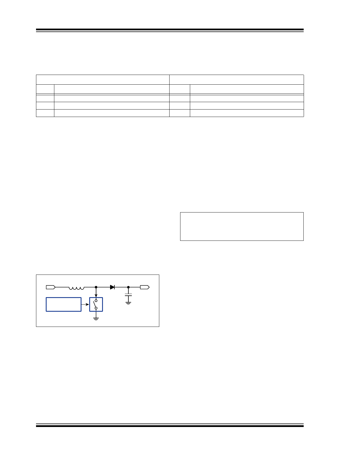
EN pin to trigger the device to select an external
voltage reference. If no enable control signal is
available in the application, this signal can be easily
mimicked by a simple RC circuit. See
Figure 4-2
.