
2016 Microchip Technology Inc.
DS20005505A-page 1
Features
• Input Voltage Range of V
DD
Regulator
- HV9110: 10V to 120V
- HV9112: 9V to 80V
- HV9113: 10V to 120V
• Maximum Duty, Feedback Accuracy
- HV9110: 49%, 1%
- HV9112: 49%, 2%
- HV9113: 99%, 1%
• Current Mode Control
• <1 mA Supply Current
• >1 MHz clock
Applications
• DC/DC Power Converters
General Description
HV9110/HV9112/HV9113 are Switch-Mode Power
Supply (SMPS) controllers suitable for the control of a
variety of converter topologies, including the flyback
converter and the forward converter.
The V
DD
regulator supports an input voltage as high as
80V or 120V.
HV9110/HV9112/HV9113 controllers include all essen-
tials for a power converter design, such as a bandgap
reference, an error amplifier, a ramp generator, a high-
speed PWM comparator, and a gate driver. A shutdown
latch provides on/off control.
The HV9110 and HV9113 feature an input voltage
range of 10V to 120V, and the HV9112 has an input
voltage range of 9V to 80V. The HV9110 and HV9112
have a maximum duty of 49%, while the HV9113 has a
maximum duty of 99%.
Package Type
See
Table 3-1
for pin information.
1
14
14-lead SOIC
HV9110/HV9112/HV9113
High-Voltage Current-Mode PWM Controller
HV9110/HV9112/HV9113
DS20005505A-page 2
2016 Microchip Technology Inc.
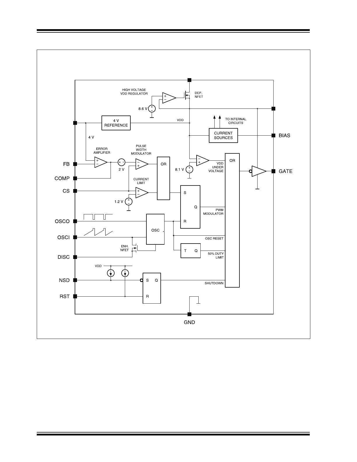
Functional Block Diagram
HV9110/HV9112
V
DD
V
IN
V
REF
2016 Microchip Technology Inc.
DS20005505A-page 3
HV9110/HV9112/HV9113
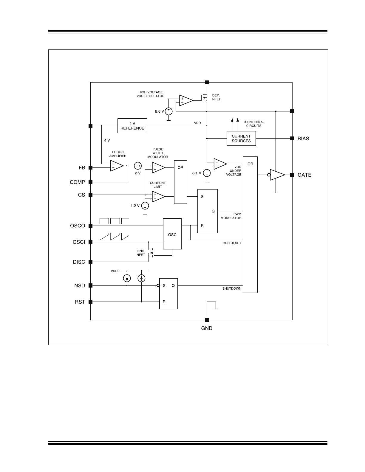
Functional Block Diagram
HV9113
V
IN
V
REF
V
DD
HV9110/HV9112/HV9113
DS20005505A-page 4
2016 Microchip Technology Inc.
1.0
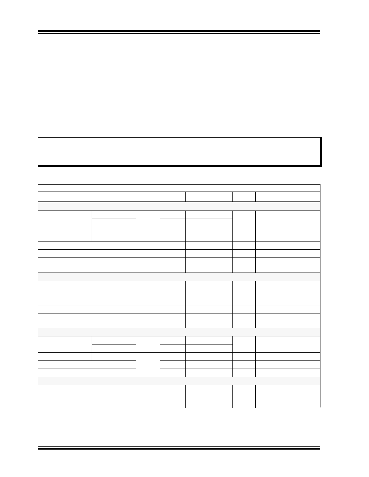
ELECTRICAL CHARACTERISTICS
ABSOLUTE MAXIMUM RATINGS
†
Input Voltage, V
IN
HV9110/HV9113 ............................................................................................................................................ 120V
HV9112............................................................................................................................................................ 80V
Device Supply Voltage, V
DD
................................................................................................................................... 15.5V
Logic Input Voltage Range .............................................................................................................. –0.3V to V
DD
+ 0.3V
Linear Input Voltage Range............................................................................................................. –0.3V to V
DD
+ 0.3V
Storage Temperature Range ................................................................................................................ –65°C to +150°C
Operating Temperature Range............................................................................................................. –55°C to +125°C
Power Dissipation: 14-lead SOIC....................................................................................................................... 750 mW
† Notice: Stresses above those listed under “Maximum Ratings” may cause permanent damage to the device. This is
a stress rating only and functional operation of the device at those or any other conditions above those indicated in the
operational listings of this specification is not implied. Exposure to maximum rating conditions for extended periods
may affect device reliability.
ELECTRICAL CHARACTERISTICS
Electrical Specifications: V
DD
= 10V, V
IN
= 48V, V
DISC
= 0V, R
BIAS
= 390 kΩ, R
OSC
= 330 kΩ, T
A
= 25°C unless otherwise noted.
Parameters
Sym.
Min.
Typ.
Max.
Units
Conditions
REFERENCE
Output Voltage
HV9110/13
V
REF
3.92
4
4.08
V
R
L
= 10 MΩ
HV9112
3.88
4
4.12
HV9110/13
3.82
4
4.16
R
L
= 10 MΩ,
T
A
= –55°C to +125°C
Output Impedance
Z
OUT
15
30
45
kΩ
(
Note 1
)
Short Circuit Current
I
SHORT
—
125
250
μA
V
REF
= GND
Change in V
REF
with Temperature
∆V
REF
—
0.25
—
mV/°C T
A
= –55°C to +125°C
(
Note 1
)
OSCILLATOR
Oscillator Frequency
f
MAX
1
3
—
MHz
R
OSC
= 0Ω
Initial Accuracy
f
OSC
80
100
120
kHz
R
OSC
= 330 kΩ (
Note
)
160
200
240
R
OSC
= 150 kΩ (
Note
)
V
DD
Regulation
—
—
—
15
%
9.5V < V
DD
< 13.5V
Temperature Coefficient
—
—
170
—
ppm/°C T
A
= –55°C to +125°C
(
Note 1
)
PWM
Maximum Duty
Cycle
HV9110/HV9112
D
MAX
49
49.4
49.6
%
(
Note 1
)
HV9113
95
97
99
Dead Time
HV9113
D
MIN
—
225
—
ns
HV9113 only (
Note 1
)
Minimum Duty Cycle
—
—
0
%
Pulse Width where Pulse drops out
—
80
125
ns
(
Note 1
)
CURRENT LIMIT
Maximum Input Signal
V
LIM
1
1.2
1.4
V
V
FB
= 0V
Delay to Output
t
D
—
80
120
ns
V
CS
= 1.5V, V
COMP
≤ 2V
(
Note 1
)
2016 Microchip Technology Inc.
DS20005505A-page 5
HV9110/HV9112/HV9113
Note 1: Design guidance only; Not 100% tested in production.
2: Stray capacitance on OSC input pin must be ≤5 pF.
ERROR AMPLIFIER
Feedback Voltage
HV9110/13
V
FB
3.96
4
4.04
V
V
FB
shorted to COMP
HV9112
3.92
4
4.08
Input Bias Current
I
IN
—
25
500
nA
V
FB
= 4V
Input Offset Voltage
V
OS
Nulled during trim
—
Open-loop Voltage Gain
A
VOL
60
80
—
dB
(
Note 1
)
Unity Gain Bandwidth
GB
1
1.3
—
MHz
(
Note 1
)
Output Source Current
I
SOURCE
–1.4
–2
—
mA
V
FB
= 3.4V
Output Sink Current
I
SINK
0.12
0.15
—
mA
V
FB
= 4.5V
HIGH-VOLTAGE REGULATOR AND START-UP
Input Voltage
HV9110/13
V
IN
—
—
120
V
I
IN
< 10 µA; V
CC
> 9.4V
HV9112
—
—
80
Input Leakage Current
I
IN
—
—
10
μA
V
DD
> 9.4V
Regulator Turn-off Threshold Voltage
V
TH
8
8.7
9.4
V
I
IN
= 10 µA
Undervoltage Lockout
V
LOCK
7
8.1
8.9
V
SUPPLY
Supply Current
I
DD
—
0.75
1
mA
C
L
< 75 pF
Quiescent Supply Current
I
Q
—
0.55
—
mA
V
NSD
= 0V
Nominal Bias Current
I
BIAS
—
20
—
μA
Operating Range
V
DD
9
—
13.5
V
SHUTDOWN LOGIC
Shutdown Delay
t
SD
—
50
100
ns
C
L
= 500 pF, V
CS
= 0V
(
Note 1
)
NSD Pulse Width
t
SW
50
—
—
ns
(
Note 1
)
RST Pulse Width
t
RW
50
—
—
ns
(
Note 1
)
Latching Pulse Width
t
LW
25
—
—
ns
V
NSD
, V
RST
= 0V(
Note 1
)
Input Low Voltage
V
IL
—
—
2
V
Input High Voltage
V
IH
7
—
—
V
Input Current, Input High Voltage
I
IH
—
1
5
μA
V
IN
= V
DD
Input Current, Input Low Voltage
I
IL
—
–25
–35
μA
V
IN
= 0V
OUTPUT
Output High Voltage HV9110/13
V
OH
V
DD
–0.25
—
—
V
I
OUT
= 10 mA
HV9112
V
DD
–0.3
—
—
HV9110/13
V
DD
–0.3
—
—
I
OUT
= 10 mA,
T
A
= –55°C to 125°C
Output Low Voltage
All
V
OL
—
—
0.2
V
I
OUT
= –10 mA
HV9110/13
—
—
0.3
I
OUT
= –10 mA,
T
A
= –55°C to 125°C
Output Resistance
Pull up
R
OUT
—
15
25
Ω
I
OUT
= ±10 mA
Pull down
—
8
20
Pull up
—
20
30
Ω
I
OUT
= ±10 mA,
T
A
= –55°C to 125°C
Pull down
—
10
30
Rise Time
t
R
—
30
75
ns
C
L
= 500 pF (
Note 1
)
Fall Time
t
F
—
20
75
ns
C
L
= 500 pF (
Note 1
)
ELECTRICAL CHARACTERISTICS (CONTINUED)
Electrical Specifications: V
DD
= 10V, V
IN
= 48V, V
DISC
= 0V, R
BIAS
= 390 kΩ, R
OSC
= 330 kΩ, T
A
= 25°C unless otherwise noted.
Parameters
Sym.
Min.
Typ.
Max.
Units
Conditions
TEMPERATURE SPECIFICATIONS
Parameters
Sym.
Min.
Typ.
Max.
Units
Conditions
TEMPERATURE RANGES
Operating Temperature
—
–55
—
125
°C
Storage Temperature
—
–65
—
150
°C
PACKAGE THERMAL RESISTANCE
14-lead SOIC
θ
ja
—
83
—
°C/W
HV9110/HV9112/HV9113
DS20005505A-page 6
2016 Microchip Technology Inc.
1.1
Truth Table
TRUTH TABLE
SHUTDOWN
RESET
OUTPUT
H
H
Normal operation
H
H → L
Normal operation, no change
L
H
Off, not latched
L
L
Off, latched
L → H
L
Off, latched, no change
2016 Microchip Technology Inc.
DS20005505A-page 7
HV9110/HV9112/HV9113
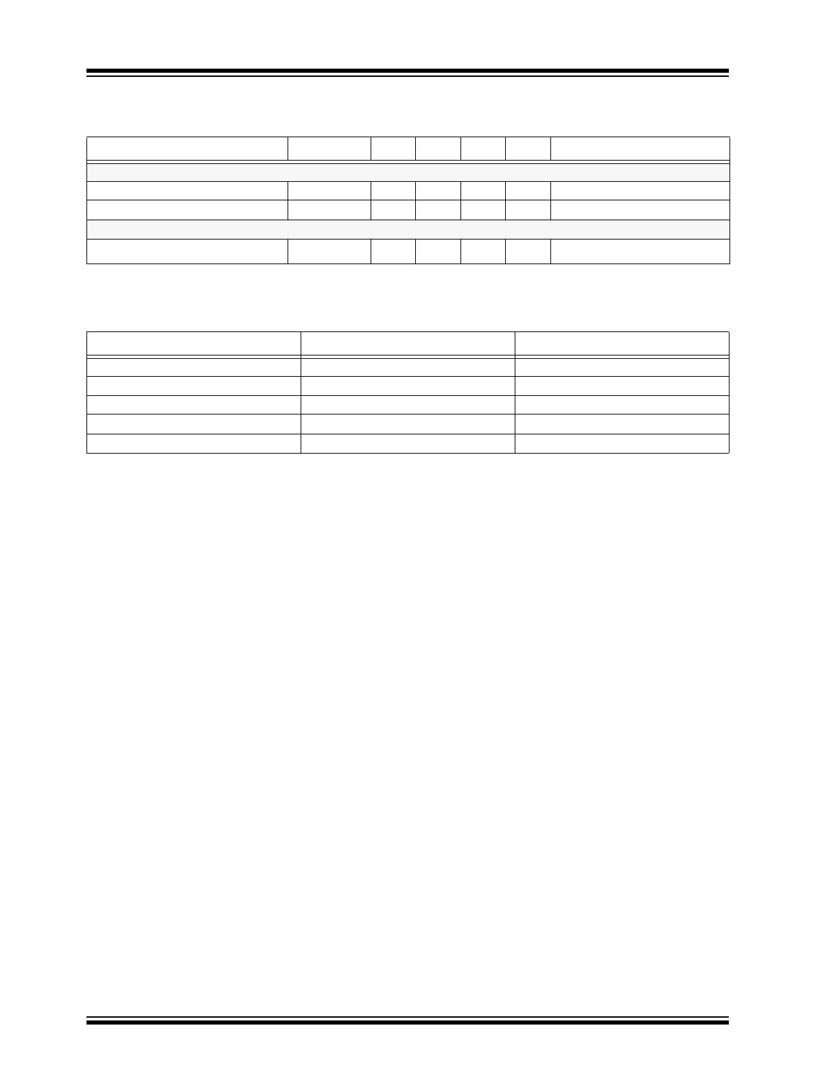
2.0
TYPICAL PERFORMANCE CURVES
Note:
The graphs and tables provided following this note are a statistical summary based on a limited number of
samples and are provided for informational purposes only. The performance characteristics listed herein
are not tested or guaranteed. In some graphs or tables, the data presented may be outside the specified
operating range (e.g. outside specified power supply range) and therefore outside the warranted range.
FIGURE 2-1:
1M
100k
10k
1k
100
10
1
100m
100 1k 10k 100k 1M 10M
Z
0
(Ω)
Frequency (Hz)
Error Amplifier Output
Impedance (Z
0
).
0
-10
-20
-30
-40
-50
-60
-70
-80
PSSR (dB)
Frequency (Hz)
10 100 1k 10k 100k 1M
FIGURE 2-2:
PSRR –Error Amplifier and
Reference.
Bias Resistance (Ω)
100k
1M
10M
Bias Current (μA)
100
10
1
V
DD
= 12V
V
DD
= 10V
FIGURE 2-3:
Bias Current vs. Bias
Resistance.
FIGURE 2-4:
10k 100k 1M
R
OSC
(Ω)
f
OUT
(Hz)
1M
100k
10k
HV9113
HV9110, HV9112
Output Switching Frequency
vs. Oscillator Resistance.
80
70
60
50
40
30
20
10
0
-10
Gain (dB)
Phase (
O
C)
180
120
60
0
-60
-120
-180
Frequency (Hz)
100 1k 10k 100k 1M
FIGURE 2-5:
Error Amplifier Open-loop
Gain/Phase.
R
DISCHARGE
(Ω)
100m 1 10 100 1k 10k 100k 1M
100
t
OFF
(ns)
1k
10k
R
OSC
= 100k
R
OSC
= 10k
R
OSC
= 1k
FIGURE 2-6:
R
DISCHARGE
vs. t
OFF
(HV9113 only).
HV9110/HV9112/HV9113
DS20005505A-page 8
2016 Microchip Technology Inc.
3.0
PIN DESCRIPTION
Table 3-1
shows the pin description for
HV9110/HV9112/HV9113. The locations of the pins are
listed in
Features
.
TABLE 3-1:
PIN DESCRIPTION
Pin Number
HV9110/HV9112/HV9113
Pin Name
Description
1
BIAS
Internal bias, current set
2
V
IN
High-voltage V
DD
regulator input
3
CS
Current sense input
4
GATE
Gate drive output
5
GND
Ground
6
V
DD
High-voltage V
DD
regulator output
7
OSCO
Oscillator output
8
OSCI
Oscillator input
9
DISC
Oscillator discharge, current set
10
V
REF
4V reference output
Reference voltage level can be overridden by an externally applied voltage
source.
11
NSD
Active low input to set shutdown latch
12
RST
Active high input to reset shutdown latch
13
COMP
Error amplifier output
14
FB
Feedback voltage input
2016 Microchip Technology Inc.
DS20005505A-page 9
HV9110/HV9112/HV9113
4.0
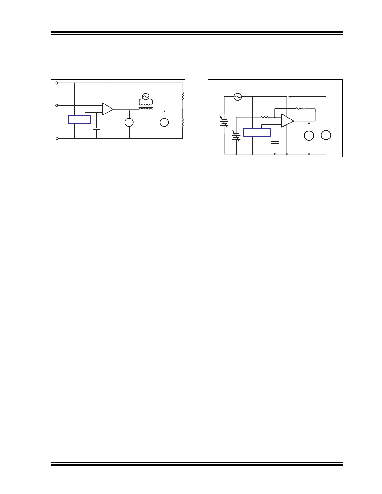
TEST CIRCUITS
The test circuits for characterizing error amplifier output impedance, Z
OUT
, and error amplifier, power supply rejection
ratio, PSRR, are shown in
Figure 4-1
and
Figure 4-2
.
+
–
Reference
60k
40k
1V swept 100 Hz-2.2 MHz
Tektronix
P6021
(1 turn
secondary)
+10 V
DD
GND
FB
NOTE:
Set Feedback Voltage so that V
COMP
= V
DIVIDE
±1 mV
before connecting transformer
100 nF
V
1
V
2
FIGURE 4-1:
Error Amp Z
OUT
.
+
–
Reference
0.1V swept
10 Hz-1.0 MHz
100 nF
10.0V
4.0V
100k1%
100k1%
V
2
V
1
FIGURE 4-2:
PSRR.

HV9110/HV9112/HV9113
DS20005505A-page 10
2016 Microchip Technology Inc.
5.0
DETAILED DESCRIPTION
5.1
High-Voltage Regulator
The high-voltage regulator included in
HV9110/HV9112/HV9113 consists of a high-voltage N-
channel Depletion-mode DMOS transistor driven by an
error amplifier, providing a current path between the
V
IN
terminal and the V
DD
terminal. The maximum cur-
rent, about 20 mA, occurs when V
DD
= 0, with current
reducing as V
DD
rises. This path shuts off when V
DD
rises to somewhere between 8V and 9.4V. So, if V
DD
is
held at 10V or 12V by an external source, no current
other than leakage is drawn through the high voltage
transistor. This minimizes dissipation within the high-
voltage regulator.
Use an external capacitor between V
DD
and GND. This
capacitor should have good high-frequency character-
istics. Ceramic caps work well.
The device uses a compound resistor divider to monitor
V
DD
for both the undervoltage lockout circuit and the
shutoff circuit of the high-voltage FET. Setting the
undervoltage sense point about 0.6V lower on the
string than the FET shutoff point guarantees that the
undervoltage lockout releases before the FET shuts
off.
5.2
Bias Circuit
HV9110/HV9112/HV9113 require an external bias
resistor, connected between the Bias pin and GND
,
to
set currents in a series of current mirrors used by the
analog sections of the chip. The nominal external bias
current requirement is 15 µA to 20 µA, which can be set
by a 390 kΩ to 510 kΩ resistor if V
DD
= 10V, or a
510 kΩ to 680 kΩ resistor if V
DD
= 12V. A precision
resistor is not required, ±5% meets device require-
ments.
5.3
Clock Oscillator
The clock oscillator of the HV9110/HV9112/HV9113
consists of a ring of CMOS inverters, timing capacitors,
and a capacitor-discharge FET. A single external resis-
tor between the OSCI and OSCO sets the oscillator fre-
quency. (See
Figure 2-4
.)
The HV9110 and HV9112 include a frequency-dividing
flip-flop that allows the part to operate with a 50% duty
limit. Accordingly, the effective switching frequency of
the power converter is half the oscillator frequency.
(See
Figure 2-4
.)
An internal discharge FET resets the oscillator ramp at
the end of the oscillator cycle. The discharge FET is
externally connected to GND, by way of a resistor. The
resistor programs the oscillator dead time at the end of
the oscillator period.
The oscillator turns off during shutdown to reduce sup-
ply current by about 150 μA.
5.4
Reference
The reference of the HV9110/HV9112/HV9113 consists
of a band-gap reference, followed by a buffer amplifier,
which scales the voltage up to 4V. The scaling resistors
of the buffer amplifier are trimmed during manufacture
so that the output of the error amplifier, when con-
nected in a gain of –1 configuration, is as close to 4V
as possible. This nulls out the input offset of the error
amplifier. As a consequence, even though the
observed reference voltage of a specific part may not
be exactly 4V, the feedback voltage required for proper
regulation will be 4V.
An approximately 50 kΩ resistor is located internally
between the output of the reference buffer amplifier
and the circuitry it feeds—reference output pin and
non-inverting input to the error amplifier. This allows
overriding the internal reference with a low impedance
voltage source ≤ 6V. Using an external reference rein-
states the input offset voltage of the error amplifier.
Overriding the reference should seldom be necessary.
The reference of the HV9110/HV9112/HV9113 is a
high-impedance node, and usually there will be signifi-
cant electrical noise nearby. Therefore, a bypass
capacitor between the reference pin and GND is
strongly recommended. The reference buffer amplifier
is compensated to be stable with a capacitive load of
0.01 µF to 0.1 µF.
5.5
Error Amplifier
The error amplifier on HV9110/HV9112/HV9113 is a
low-power, differential-input, operational amplifier. A
PMOS input stage is used, so the common mode range
includes ground and the input impedance is high.
5.6
Current Sense Comparators
The HV9110/HV9112/HV9113 use a dual-comparator
system with independent comparators for modulation
and current limiting. This provides the designer greater
latitude in compensation design, as there are no
clamps, except ESD protection, on the compensation
pin.
5.7
Remote Shutdown
The NSD and RST pins control the shutdown latch.
These pins have internal current-source pull-ups so
they can be driven from open drain logic. When not
used they should be left open or connected to V
DD
.