
2015 Microchip Technology Inc.
DS20005450A-page 1
HV825
Features
• Processed with HVCMOS
®
Technology
• 1.0 to 1.6V Operating Supply Voltage
• DC to AC Conversion
• Output Load of Typically up to 6.0 nF
• Adjustable Output Lamp Frequency
• Adjustable Converter Frequency
• Enable Function
Applications
• Pagers
• Portable Transceivers
• Cellular Phones
• Remote Control Units
• Calculators
General Description
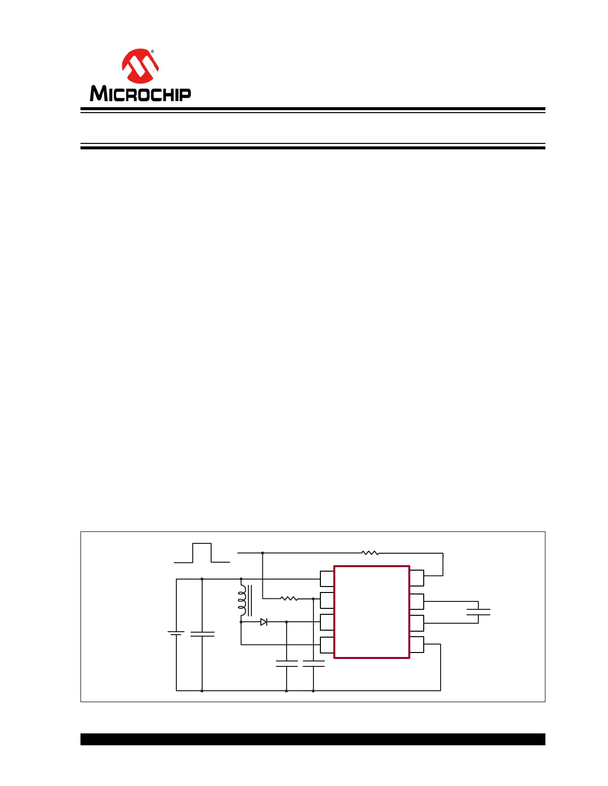
The HV825 is a high-voltage driver designed for driv-
ing EL lamps typically up to 6.0 nF. The input supply
voltage range is from 1.0V to 1.6V. The device uses a
single inductor and a minimum number of passive
components. The typical output voltage that can be
applied to the EL lamp is ±56V.
The HV825 can be enabled/disabled by connecting
the R
SW-Osc
resistor to V
DD
/GND.
The HV825 has two internal oscillators to drive a switch-
ing bipolar junction transistor (BJT), and a high-voltage
EL lamp driver. The frequency for the switching BJT is
set by an external resistor connected between the R
SW-
Osc
pin and the V
DD
supply pin. The EL lamp driver fre-
quency is set by an external resistor connected between
the R
EL-Osc
pin and the V
DD
pin. An external inductor is
connected between the L
X
and V
DD
pins. A 0.01 to
0.1 µF, 100V capacitor is connected between the C
S
pin
and the GND pin. The EL lamp is connected between
the V
A
pin and the V
B
pin.
The switching BJT charges the external inductor and
discharges it into the 0.01 to 0.1 µF, 100V capacitor at
the C
S
pin. The voltage at the C
S
pin will start to
increase. The outputs V
A
and V
B
are configured as an
H-bridge, and are switching in opposite states to
achieve a peak-to-peak voltage of two times the V
CS
voltage across the EL lamp.
Typical Application Circuit
V
DD
= V
IN
= 1.5V
0.01 μF
100V
1.0 nF
16V
560 μH
1N4148
Nȍ
0ȍ
EL Lamp
ON = V
DD
OFF = 0V
0.1 μF
2
1
7
2
3
4
8
6
5
LX
GND
VB
VA
REL-Osc
VDD
RSW-Osc
CS
High-Voltage EL Lamp Driver IC
HV825
DS20005450A-page 2
2015 Microchip Technology Inc.
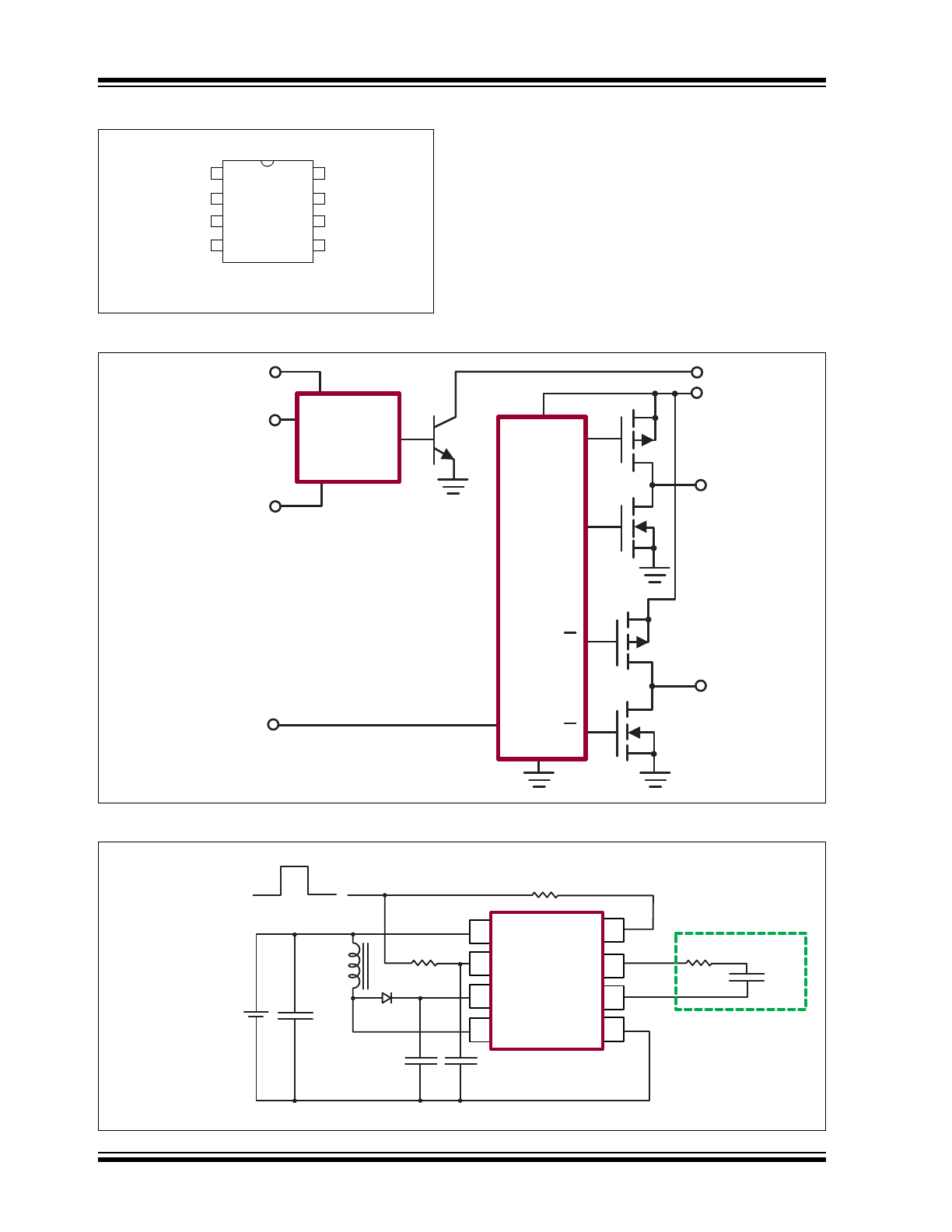
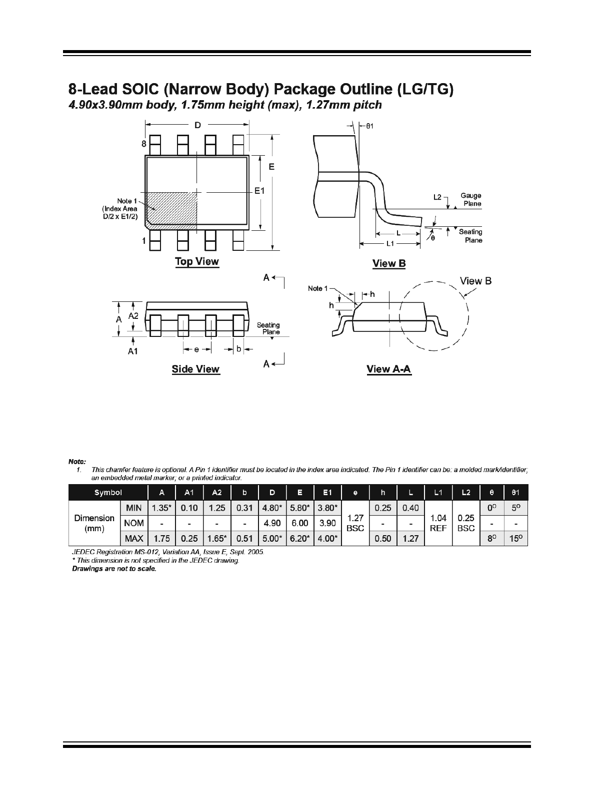
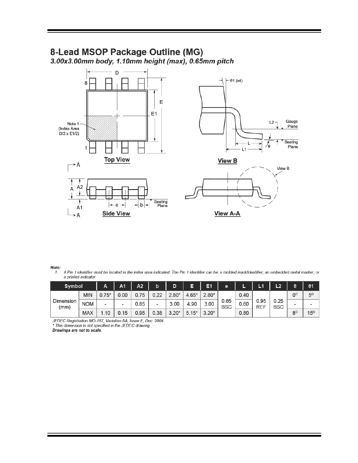
Package Types
Block Diagram
Test Circuit
V
DD
RSW-Osc
CS
LX
REL-Osc
VA
VB
GND
1
2
3
4
8
7
6
5
8-Lead SOIC / 8-Lead MSOP
GND
VDD
REL-Osc
VA
CS
LX
VB
RSW-Osc
Switch
Osc
Output
Osc
Q
Q
Q
Q
V
DD
= V
IN
= 1.0V - 1.6V
0.01 μF
100V
C
SW
1.0 nF
560 μH
1
1N4148
Nȍ
0ȍ
Nȍ
4.7 nF
ON = V
DD
OFF = GND
0.1 μF
Equivalent to
1.5 in
2
lamp
Enable
7
8
6
5
LX
GND
VB
VA
REL-Osc
VDD
RSW-Osc
CS
1
2
3
4
1:
Murata part # LGH4N561K04
2015 Microchip Technology Inc.
DS20005450A-page 3
HV825
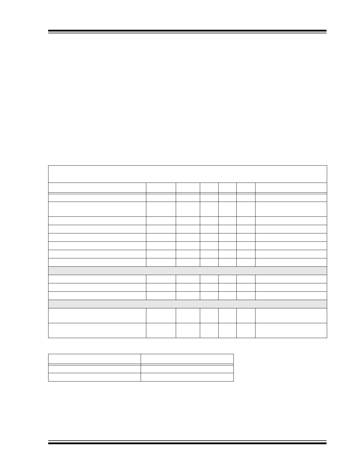
1.0
ELECTRICAL
CHARACTERISTICS
Absolute Maximum Ratings
(†)
V
DD
pin............................................................................................................................................................ 0.5 to 2.5V
Package Power Dissipation (MSOP-8) ................................................................................................................300 mW
Package Power Dissipation (SO-8)......................................................................................................................400 mW
Operating Ambient Temperature Range ...................................................................................................-25°C to +85°C
Storage Temperature Range...................................................................................................................-65°C to +150°C
† Notice: Stresses above those listed under “Absolute Maximum Ratings” may cause permanent damage to the device.
This is a stress rating only and functional operation of the device at those or any other conditions above those indicated in
the operation listings of this specification is not implied. Exposure above maximum rating conditions for extended periods
may affect device reliability
DC CHARACTERISTICS
Typical Thermal Resistance
Electrical Specifications: Unless otherwise specified, all specifications apply at T
A
= 25°C over recommended
operating conditions.
Parameters
Sym.
Min.
Typ.
Max.
Unit
Conditions
On-resistance of switching transistor
R
ON
—
—
15
Ω
I = 50 mA
V
DD
supply current
(including inductor current)
I
IN
—
30
38
mA
V
DD
= 1.5V. See test circuit.
Quiescent V
DD
supply current
I
DDQ
—
—
1.0
µA
R
SW-OSC
= GND
Output voltage on V
CS
V
CS
52
56
62
V
V
DD
= 1.5V. See test circuit.
Differential output voltage across lamp
V
A-B
104
112
124
V
V
DD
= 1.5V. See test circuit.
V
A-B
output drive frequency
f
EL
400
—
—
Hz
V
DD
= 1.5V. See test circuit.
Switching transistor frequency
f
SW
—
30
—
KHz V
DD
= 1.5V. See test circuit.
Switching transistor duty cycle
D
—
88
—
%
Recommended Operating Conditions
Supply voltage
V
DD
1.0
—
1.6
V
Load capacitance
C
L
0
6
—
nF
Operating temperature
T
A
-25
—
+85
°C
Enable/Disable Table
Low-level input voltage to
R
SW-OSC
resistor
V
IL
0
—
0.2
V
V
DD
= 1.0–1.6V
High-level input voltage to
R
SW-OSC
resistor
V
IH
V
DD
–0.5
—
V
DD
V
V
DD
= 1.0–1.6V
Package
Θ
ja
8-Lead SOIC
101°C/W
8-Lead MSOP
216°C/W
HV825
DS20005450A-page 4
2015 Microchip Technology Inc.
2.0
APPLICATION INFORMATION
2.1
Typical Performance
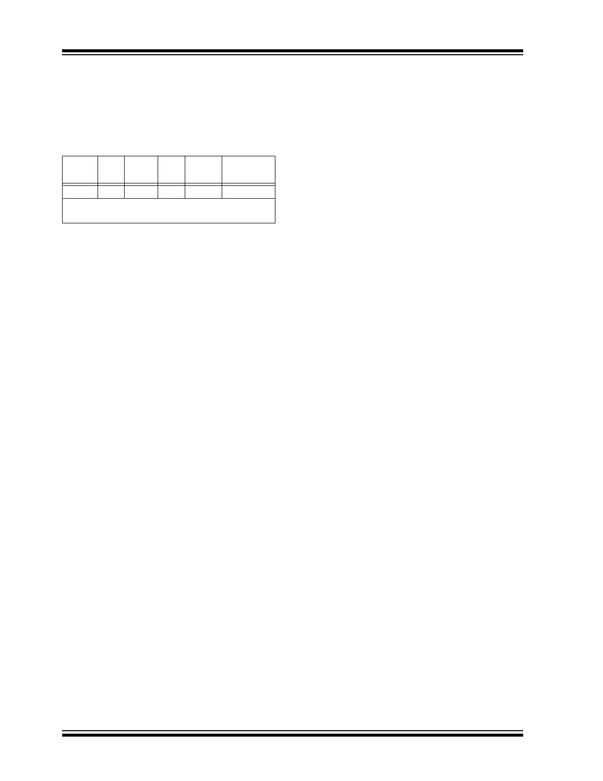
Table 2-1
shows the performance of the typical
application circuit.
2.2
Diode
A fast reverse recovery diode is used (1N4148 or
equivalent).
2.3
C
S
Capacitor
A 0.01 to 0.1 µF, 100V capacitor to GND is used to
store the energy transferred from the inductor.
2.4
R
EL-Osc
Resistor
The lamp frequency is controlled via the R
EL-Osc
pin.
The lamp frequency increases as R
EL-Osc
decreases.
As the lamp frequency increases, the amount of current
drawn from the battery will increase and the output
voltage V
CS
will decrease. This is because the lamp will
draw more current from V
CS
when driven at higher
frequencies.
In general, as the lamp size increases, a larger R
EL-Osc
is recommended to provide higher V
CS
. However, the
color of the lamp is dependent upon its frequency and
the shade of the color will change slightly with different
frequencies.
2.5
R
SW-Osc
Resistor
The switching frequency of the inductor is controlled via
the R
SW-Osc
. The switching frequency increases as the
R
SW-Osc
decreases. As the switching frequency
increases, the amount of current drawn from the
battery will decrease and the output voltage V
CS
will
also decrease.
2.6
L
X
Inductor
The inductor L
X
is used to boost the low input voltage.
When the internal switch is on, the inductor is being
charged. When the internal switch is off, the charge in
the inductor will be transferred to the high voltage
capacitor C
S
. The energy stored in the capacitor is
connected to the internal H-bridge and therefore to the
lamp. In general, smaller value inductors, which can
handle more current, are more suitable to drive larger
lamps. As the inductor value decreases, the switching
frequency of the inductor (controlled by R
SW-Osc
)
should be increased to avoid saturation.
The test circuit uses a Murata (LQH4N561) 560 µH
inductor. Using different inductor values or inductors
from different manufacturers will affect the
performance.
As the inductor value decreases, smaller R
SW-Osc
values should be used. This will prevent inductor
saturation. An inductor with the same inductance value
(560 µH) but lower series resistance will charge faster.
The R
SW-Osc
resistor value needs to be decreased to
prevent inductor saturation and high current
consumption.
2.7
C
SW
Capacitor
A 1 nF capacitor is recommended from the R
SW-Osc
pin
to GND. This capacitor is used to shunt any switching
noise that may couple into the R
SW-Osc
pin. A C
SW
larger than 1 nF is not recommended.
TABLE 2-1:
TYPICAL PERFORMANCE
Lamp
Size
V
IN
I
DD
V
CS
f
EL
Brightness
1.5 in²
1.5V 30 mA 56V
450 Hz
3.65 ft-lm
Note:
Results use Murata part # LQH4N561K04,
max DC resistance = 14.5Ω
2015 Microchip Technology Inc.
DS20005450A-page 5
HV825
3.0
PACKAGING INFORMATION
3.1
Package Marking Information
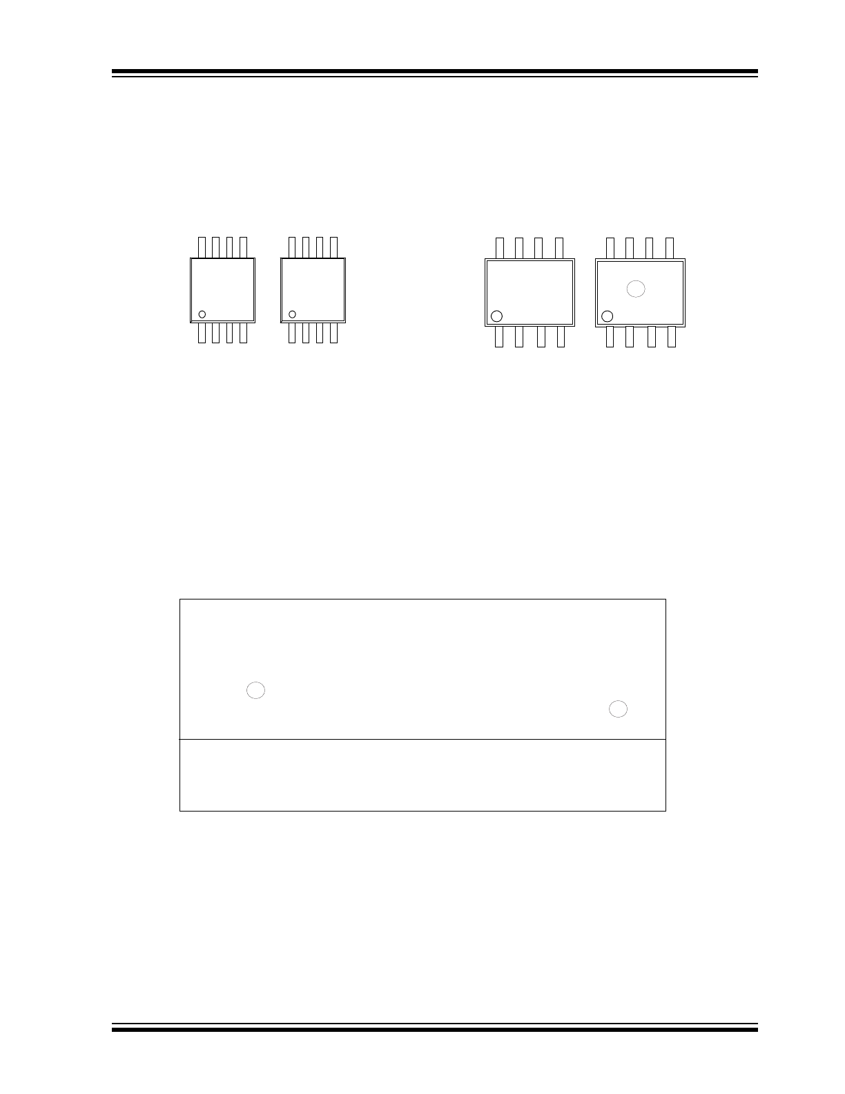
8-Lead MSOP*
XXXXX
YWWNNN
Example:
Example:
HV825
5011L7
8-Lead SOIC*
XXXXXXX
NNN
1343
HV825LG
1L7
3
e
^^YYWW
Legend: XX...X
Product Code or Customer-specific information
Y
Year code (last digit of calendar year)
YY
Year code (last 2 digits of calendar year)
WW
Week code (week of January 1 is week ‘01’)
NNN
Alphanumeric traceability code
Pb-free JEDEC
®
designator for Matte Tin (Sn)
*
This package is Pb-free. The Pb-free JEDEC designator ( )
can be found on the outer packaging for this package.
Note:
In the event the full Microchip part number cannot be marked on one line, it will
be carried over to the next line, thus limiting the number of available
characters for product code or customer-specific information. Package may or
not include the corporate logo.
3
e
3
e
HV825
DS20005450A-page 6
2015 Microchip Technology Inc.
Note: For the most current package drawings, see the Microchip Packaging Specification at www.microchip.com/packaging
2015 Microchip Technology Inc.
DS20005450A-page 7
HV825
Note: For the most current package drawings, see the Microchip Packaging Specification at www.microchip.com/packaging.

HV825
DS20005450A-page 8
2015 Microchip Technology Inc.
APPENDIX A: REVISION HISTORY
Revision A (November 2015)
• Initial release of this document in the Microchip
format. This replaces version CO72913.
2015 Microchip Technology Inc.
DS20005450A-page 9
HV825
PRODUCT IDENTIFICATION SYSTEM
To order or obtain information, e.g., on pricing or delivery, refer to the factory or the listed sales office
.
PART NO.
X
XX
Package
Environmental
Device
Device:
HV825
=
High Voltage EL Lamp Driver IC
Package:
LG
=
MG
=
8-lead SOIC
8-lead MSOP
Environmental:
G
=
Lead (Pb)-free/ROHS-compliant Package
Media Type:
(blank)
=
2500/Reel for LG and MG packages
Examples:
a) HV825LG-G:
High Voltage EL Lamp Driver IC
8-lead SOIC package, 2500/reel
b) HV825MG-G:
High Voltage EL Lamp Driver IC
8-lead MSOP package, 2500/reel
–
Options
X
Media Type
–

HV825
DS20005450A-page 10
2015 Microchip Technology Inc.
NOTES: